

Page 1
NCV78825
f
T
High Efficiency 3 A
Synchronous Buck Dual
LED Driver with Integrated
High Side Switch and
Current Sensing for
www.onsemi.com
Automotive Front Lighting
Description
The NCV78825 is a single−chip and high efficient Synchronous
Buck Dual LED Driver designed for automotive front lighting
applications like high beam, low beam, DRL (daytime running light),
turn indicator, fog light, static cornering, etc. The NCV78825 is in
particular designed for high current LEDs and provides a complete
solution to drive 2 LED strings of up−to 60 V. It includes 2
independent current regulators for the LED strings and required
diagnostic features for automotive front lighting with a minimum of
external components – the chip doesn’t need any external sense
resistor for the buck current regulation. The available output current
and voltages can be customized per individual LED string. When more
than 2 LED channels are required on 1 module, then 2, 3 or more
devices NCV78825 can be combined; also with NCV787x3 devices –
the predecessor of the NCV78825. Thanks to the SPI
programmability, one single hardware configuration can support
various application platforms.
Features
A = Assembly Location
WL = Wafer Lot
YY = Year
WW = Work Week
G = Pb−Free Package
• Single Chip
• Buck Topology
• 2 LED Strings up−to 60 V
• High Current Capability up to 3 A DC per Output
See detailed ordering and shipping information on page 2 o
this data sheet.
ORDERING INFORMATION
• Integrated High Side Switch
• Low Side Pre−driver for External NMOS Device
• High Overall Efficiency
• Minimum of External Components
• Integrated High Accuracy Current Sensing
• Integrated Switched Mode Buck Current Regulator
• Average Current Regulation Through the LEDs
• High Operating Frequencies to Reduce Inductor Sizes
• Low EMC Emission for LED Switching and Dimming
ypical Applications
• High Beam
• Low Beam
• DRL
• Position or Park Light
• Turn Indicator
• Fog
• Static Cornering
• SPI Interface for Dynamic Control of System Parameters
• Fail Safe Operating (FSO) Mode, Stand−Alone Mode
• Master−Slave Synchronization Mode of the Buck Channels
• NCV Prefix for Automotive and Other Applications Requiring
Unique Site and Control Change Requirements; AEC−Q100
Qualified and PPAP Capable
• This is a Pb−Free Device
SSOP36 EP
CASE 940AB
MARKING DIAGRAM
NV78825−0
AWLYYWWG
© Semiconductor Components Industries, LLC, 2017
February, 2018 − Rev. 1
1 Publication Order Number:
NCV78825/D
Page 2
NCV78825
ORDERING INFORMATION
Table 1. AVAILABLE PART NUMBERS
Device Marking Package* Shipping
NCV78825DQ0R2G NV78825−0 SSOP36 EP
1500 / Tape & Reel
(PbFree)
*For additional information on our Pb−Free strategy and soldering details, please download the ON Semiconductor Soldering and Mounting
Techniques Reference Manual, SOLDERRM/D.
†For information on tape and reel specifications, including part orientation and tape sizes, please refer to our Tape and Reel Packaging
Specification Brochure, BRD8011/D.
TYPICAL APPLICATION SCHEMATIC
VBOOST
C_M3V
†
μC
VIO of MCU
R_SDO
VDRIVE
C_DRV
C_DD
VINBCK1
VBOOST
LBCKSW1
VDRIVE
VDD_C
RSTB
LEDCTRL1
LEDCTRL2
SCLK
SDI
SDO
CSB
TEST
NCV78825
TEST1
TEST2
VBOOSTM3V
GND
LSFET1
GNDS1
VLED1
VINBCK2
LBCKSW2
LSFET2
GNDS2
VLED2
EXPOSED
PAD
R_LED_1
R_LED_2
Figure 1. Typical Application Schematic
L_BCK_1
T_LS 1
C_LED_1
L_BCK_2
T_LS 2
C_LED_2
LED−string 1
C_BCK_1
LED−string 2
C_BCK_2
www.onsemi.com
2
Page 3

NCV78825
Table 2. EXTERNAL COMPONENTS
Component
L_BCK_x Buck regulator coil (see BUCK REGULATOR chapter for details) 47 (22) μH
C_BCK_x
C_M3V
C_DD
C_DRV
C_LED_x
R_LED_x
R_SDO
T_LSx
1. Pin TEST has to be connected to ground. TEST1 and TEST2 pins can be connected to ground or left floating.
2. C_LED_x is optional. If used, time constant of the C_LED_x and R_LED_x filter has to be lower than minimal LEDCTRLx PWM time for proper
VLED measurement.
3. R_LED_x is necessary to ensure Absolute maximum ratings of IVLEDx current (see Table 4).
4. GNDSx pins have to be star connections to the corresponding S of the external LS FET.
Buck regulator output capacitor (see BUCK REGULATOR chapter for details) 220 nF
Capacitor for M3V regulator 470 (see Table 8) nF
VDD decoupling capacitor 470 (see Table 7) nF
V
decoupling capacitor 470 nF
DRIVE
Optional VLEDx pin filter capacitor (Note 2) 1 nF
VLEDx pin serial resistor (Notes 2 and 3) 1 kΩ
SPI pull−up resistor 1 kΩ
Buck regulator low side switch (LS FET) NVTFS5C680NL,
Function Typ. Value Unit
NVMFS5C673NL
www.onsemi.com
3
Page 4
NCV78825
VDRIVE
(4.5 V – 10 V)
VDD_C
LEDCTRL1
LEDCTRL2
RSTB
SDI
SCLK
CSB
SDO
TEST
TEST1
TEST2
VGATE
LDO
Bandgap
POR
Bias
OSC
5 V input
5 V input/
OD output
LV IOs
2−Channel Buck
Vref
Digital control
ADC
MUX
Dividers
Temp
OTP
CTRL
CTRL
VBOOSTM3V
regulator
Current
sense CMP
Predriver
VGATE
Current
sense CMP
Predriver
VGATE
VBOOST
VBOOSTM3V
VINBCK11
VINBCK12
LBCKSW11
LBCKSW12
LSFET1
GNDS1
VLED1
VINBCK21
VINBCK22
LBCKSW21
LBCKSW22
LSFET2
GNDS2
VLED2
EXPOSED PAD
VDD,
VLEDx
VBOOST,
GND
Figure 2. Block Diagram
www.onsemi.com
4
Page 5
NCV78825
RSTB
SDO
SCLK
SDI
CSB
LSFET1
GNDS1
NC
VBOOST
VBOOSTM3V
NC
10
11
1
2
3
4
5
6
7
8
9
36
35
34
33
32
31
30
29
28
27
26
LEDCTRL1
LEDCTRL2
TEST
TEST1
VDRIVE
LSFET2
GNDS2
GND
TEST2
VDD_C
NC
LBCKSW11
LBCKSW12
NC
VLED1
NC
VINBCK11
VINBCK12
12
13
14
15
16
SELF PROT PDMOS
17
18
Figure 3. ESD Schematic
SELF PROT PDMOS
25
24
23
22
21
20
19
LBCKSW21
LBCKSW22
NC
VLED2
NC
VINBCK21
VINBCK22
www.onsemi.com
5
Page 6
RSTB
1
SDO
2
3
SCLK
4
SDI
5
CSB
LSFET1
6
GNDS1
7
NC
8
9
VBOOST
10
VBOOSTM3V
NC
11
12
LBCKSW11
13
LBCKSW12
14
NC
15
VLED1
16
NC
17
VINBCK11
18
VINBCK12
NCV78825
LEDCTRL1
LEDCTRL2
TEST
TEST1
VDRIVE
LSFET2
GNDS2
GND
TEST2
VDD_C
NC
LBCKSW21
LBCKSW22
NC
VLED2
NC
VINBCK21
VINBCK22
36
35
34
33
32
31
30
29
28
27
26
25
24
23
22
21
20
19
Figure 4. Pin Connections − SSOP36−EP (Top View)
Table 3. PIN DESCRIPTION
Pin No.
SSOP36−EP
VBOOST Supply
Voltage
1
2 SDO SPI data output MV open−drain
3 SCLK SPI clock MV in
4 SDI SPI data input MV in
5 CSB SPI chip select (chip select bar) MV in
6 LSFET1 Buck 1 driver output for ext. low side switch MV out
7 GNDS1 Buck 1 ground sense for ext. low side switch MV out
8, 11, 14, 16, 21, 23, 26 GND/NC GND/NC connection in application NC
9 VBOOST Booster input voltage pin HV supply
10 VBOOSTM3V VBOOSTM3V regulator output pin HV out (supply)
12 LBCKSW11 Buck 1 switch output HV out
13 LBCKSW12 Buck 1 switch output HV out
15 VLED1 LED String 1 Forward Voltage Sense Input HV in
17 VINBCK11 Buck 1 high voltage supply HV supply
18 VINBCK12 Buck 1 high voltage supply HV supply
19 VINBCK22 Buck 2 high voltage supply HV supply
20 VINBCK21 Buck 2 high voltage supply HV supply
22 VLED2 LED String 2 Forward Voltage Sense Input HV in
24 LBCKSW22 Buck 2 switch output HV out
Pin Name Description I/O Type
RSTB External reset signal MV in
www.onsemi.com
6
Page 7

NCV78825
Table 3. PIN DESCRIPTION (continued)
Pin No.
SSOP36−EP
25 LBCKSW21 Buck 2 switch output HV out
27 VDD_C 3.3 V logic supply LV supply
28 TEST2 Internal function. To be tied to GND or left open LV in/out
29 GND Ground Ground
30 GNDS2 Buck 2 ground sense for ext. low side switch MV out
31 LSFET2 Buck 2 driver output for ext. low side switch MV out
32 VDRIVE Pre−driver supply MV supply
33 TEST1 Internal function. To be tied to GND or left open LV in/out
34 TEST Internal function. To be tied to GND LV in
35 LEDCTRL2 LED string 2 enable MV in
36 LEDCTRL1 LED string 1 enable MV in
EP EXPOSED PAD To be tied to GND
Table 4. ABSOLUTE MAXIMUM RATINGS
Characteristic
VBOOST Supply Voltage V
VINBCKx Supply Voltage (Note 1) VINBCKx Max of
VBOOSTM3V Supply Voltage (Note 2) VBOOSTM3V Max of V
VDRIVE Supply Voltage VDRIVE −0.3 12 V
LSFETx Voltage (Note 3) LSFETx −0.3 Min of VDRIVE + 0.3, 12 V
VLED Sense Voltage VLEDx −0.3 Min of V
Logic Supply Voltage (Note 4) V
Medium Voltage IO Pins IOMV −0.3 7.0 V
Test Pins (Note 5) TESTx −0.3 Min of V
Buck Switch Low Side (Note 1) LBCKSWx −2 VINBCKx + 0.3 V
VLED Sink/source Current IVLEDx −30 30 mA
Storage Temperature (Note 6) T
The Exposed Pad (Note 7) EXPAD GND − 0.3 GND + 0.3 V
The LS Pre−driver Sense GND Voltage GNDSx GND − 0.3 GND + 0.3 V
Electrostatic Discharge on Component
Level Human Body Model (Note 8)
Electrostatic Discharge on Component
Level Charge Device Model (Note 8)
Stresses exceeding those listed in the Maximum Ratings table may damage the device. If any of these limits are exceeded, device functionality
should not be assumed, damage may occur and reliability may be affected.
1. V(VINBCKx − LBCKSWx) < 70 V, the driver in off state.
2. The VBOOSTM3V regulator in off state.
3. The LSFETx driver in HiZ state.
4. Absolute maximum rating for pins: VDD, TEST. Also valid for relative difference VBOOST − VBOOSTM3V.
5. Absolute maximum rating for pins: TEST1, TEST2.
6. For limited time up to 100 hours. Otherwise the max storage temperature is 85°C.
7. The exposed pad must be hard wired to GND pin in the application to ensure both electrical and thermal connection.
8. This device series incorporates ESD protection and is tested by the following methods:
ESD Human Body Model tested per AECQ100002 (EIA−JESD22A114−B)
ESD Charge Device Model tested per EIA−JESD22C101
Latchup Current Maximum Rating: 100 mA per JEDEC standard: JESD78
Symbol Min Max Unit
BOOST
DD
STRG
V
ESD_HBM
V
ESD_CDM
VBOOSTM3V − 0.3, −0.3
−0.3 68 V
Min of V
BOOST
− 3.6, −0.3 Min of V
BOOST
BOOST
BOOST
−0.3 3.6 V
DD
−50 150 °C
−2 +2 kV
−500 +500 V
I/O TypeDescriptionPin Name
+ 0.3, 68 V
+ 0.3, 68 V
+ 0.3, 68 V
+ 0.3, 3.6 V
www.onsemi.com
7
Page 8

NCV78825
Operating ranges define the limits for functional
operation and parametric characteristics of the device. A
mission profile (Note 1) is a substantial part of the operation
conditions; hence the Customer must contact
ON Semiconductor in order to mutually agree in writing on
the allowed missions profile(s) in the application.
Table 5. RECOMMENDED OPERATING RANGES
Characteristic
Boost Supply Voltage V
VINBCKx Supply Voltage (Note 2) VINBCKx V
VDRIVE Voltage Supply VDRIVE 4.5 10 V
Buck Switch Peak Output Current I_LBCKSW 3.8 A
Functional Operating Junction
Temperature Range (Note 3)
Parametric Operating Junction
Temperature Range (Note 4)
The Exposed Pad Connection (Note 5) EXPOSED_PAD GND − 0.1 GND GND + 0.1 V
The LS Pre−driver Sense GND Voltage
(Note 6)
Functional operation above the stresses listed in the Recommended Operating Ranges is not implied. Extended exposure to stresses beyond
the Recommended Operating Ranges limits may affect device reliability.
1. A mission profile describes the application specific conditions such as, but not limited to, the cumulative operating conditions over life time,
the system power dissipation, the system’s environmental conditions, the thermal design of the customer’s system, the modes, in which the
device is operated by the customer, etc. No more than 100 cumulated hours in life time above T
2. Hard connection of VINBCKx to VBOOST on PCB.
3. The circuit functionality is not guaranteed outside the functional operating junction temperature range. Also please note that the device is
verified on bench for operation up to 170°C but that the production test guarantees 155°C only.
4. The parametric characteristics of the circuit are not guaranteed outside the Parametric operating junction temperature range.
5. The exposed pad must be hard wired to GND pin in an application to ensure both electrical and thermal connection.
6. The hard connection of the GNDSx pins on the PCB, mainly to the S of the LS NMOS device
corresponding S of the LS NMOS max +/− 0.2 mV.
Symbol Min Typ Max Unit
BOOST
T
JF
T
JP
GNDSx GND − 0.1 GND GND + 0.1 mV
6 67 V
− 0.1 V
BOOST
−40 155 °C
−40 150 °C
BOOST
V
.
tw
+ 0.1 V
BOOST
the voltage difference between the pin and
Table 6. THERMAL RESISTANCE
Characteristic
Thermal Resistance Junction to Exposed Pad (Note 1) SSOP36−EP Rthjp − 3.5 − °C/W
1. Includes also typical solder thickness under the Exposed Pad (EP).
Package Symbol Min Typ Max Unit
www.onsemi.com
8
Page 9

NCV78825
ELECTRICAL CHARACTERISTICS
Table 7. VDD: 3.3 V LOW VOLTAGE ANALOG AND DIGITAL SUPPLY
Characteristic Symbol Conditions Min Typ Max Unit
The Regulator Output Voltage VDD 3.05 3.45 3.6 V
VDD External Decoupling Cap C_DD 0.3 0.47 2.2 μF
The VDRIVE Current Consumption (Note 2) I_VDRIVE 8 15 mA
Output Current Limitation VDD_ILIM 15 160 mA
POR Toggle Level on VDD Rising POR
POR Toggle Level on VDD Falling POR
POR Hysteresis POR
OTP UV Toggle Level on VBOOST OTP_UV 13 15 V
OTP UV Toggle Level Hysteresis OTP_UV_HYST 0.01 0.2 0.75 V
1. All Min and Max parameters are guaranteed over full junction temperature (TJP) range (−40 °C; 150 °C), unless otherwise specified.
2. Only internal consumption, Excluding LS NMOS gate charge current.
3V_H
3V_L
3V_HYST
Table 8. VBOOSTM3V: HIGH SIDE AUXILIARY SUPPLY
Characteristic
VBOOSTM3V Regulator Output Voltage V
DC Output Current Capability (Note 1) M3V_IOUT 7.5 42 mA
Output Current Limitation M3V_ILIM 300 mA
VBOOSTM3V External Decoupling Cap C_M3V Referenced to VBOOST 0.1 0.47 2.2
VBOOSTM3V Ext. Decoupling Cap. ESR C_M3V_ESR Referenced to VBOOST 200
VBSTM3V POR Level, Falling Edge M3V_PORL Referenced to VBOOST −2.7 −1.8 V
VBSTM3V POR Level, Rising Edge M3V_PORH Referenced to VBOOST −2.4 −1.8 V
VBSTM3V POR Level Hysteresis M3V_PORHYST 0.05 V
VBOOST POR Level M3V_VBSTPOR VBOOST goes down 3.5 5.5 V
1. VBOOST = 68 V, f
= 2 MHz, maximum total gate charge for both activated BUCK channels Qgate = 20 nC
BUCK
Symbol Conditions Min Typ Max Unit
BSTM3V
Referenced to VBOOST −3.6 −3.3 −3.0 V
2.7 3.05 V
2.45 2.8 V
0.01 0.2 0.75 V
mF
mW
Table 9. OSC10M: SYSTEM OSCILLATOR CLOCK
Characteristic Symbol Conditions Min Typ Max Unit
System Oscillator Frequency FOSC10M 8 10 12 MHz
Table 10. ADC FOR MEASURING VBOOST, VDD, VLED1, VLED2, TEMP
Characteristic
ADC Resolution ADC_RES 8 Bits
Integral Nonlinearity (INL) ADC_INL Best fitting straight line method −1.5 1.5 LSB
Differential Nonlinearity (DNL) ADC_DNL Best fitting straight line method −2 2 LSB
Full Path Gain Error for
Measurements of VLEDx,
VBOOST
Offset at Output of ADC ADC_OFFS −2 2 LSB
Time for 1 SAR Conversion ADC_CONV Full conversion of 8 bits 6.67 8 10
ADC Full Scale for VDD
Measurement
ADC Full Scale for VLEDx
Measurement
ADC Full Scale for VLEDx
Measurement
ADC Full Scale for VLEDx
Measurement
Symbol Conditions Min Typ Max Unit
ADC_GE −3.25 3.25 %
ADCFS_VDD 3.87 4 4.13 V
ADCFS_VLED00 The VLED range code is “00” 67.725 70 72.275 V
ADCFS_VLED01 The VLED range code is “01” 48.375 50 51.625 V
ADCFS_VLED10 The VLED range code is “10” 38.700 40 41.300 V
ms
www.onsemi.com
9
Page 10

NCV78825
Table 10. ADC FOR MEASURING VBOOST, VDD, VLED1, VLED2, TEMP (continued)
Characteristic UnitMaxTypMinConditionsSymbol
ADC Full Scale for VLEDx
Measurement
ADC Full Scale for VBOOST
Measurement
TSD Threshold Level ADC_TSD ADC measurement of junction
Temperature measurement
accuracy at hot
Temperature measurement
accuracy at cold
VLED Input Impedance VLED_RES 280 790
Table 11. BUCK REGULATOR – SWITCH
Characteristic Symbol Conditions Min Typ Max Unit
On Resistance, Range 1 RON1 At room−temperature, I(VINBCKx) = 0.18 A,
On Resistance at Hot, Range 1 RON1_H At Tj = 160 °C, I(VINBCKx) = 0.18 A,
On Resistance, Range 2 RON2 At room−temperature, I(VINBCKx) = 0.375 A,
On Resistance at Hot, Range 2 RON2_H At Tj = 160 °C, I(VINBCKx) = 0.375 A,
On Resistance, Range 3 RON3 At room−temperature, I(VINBCKx) = 0.75 A,
On Resistance at Hot, Range 3 RON3_H At Tj = 160 °C, I(VINBCKx) = 0.75 A,
On Resistance, Range 4 RON4 At room−temperature, I(VINBCKx) = 1.5 A,
On Resistance at Hot, Range 4 RON4_H At Tj = 160 °C, I(VINBCKx) = 1.5 A,
On Resistance, Range 5 RON5 At room−temperature, I(VINBCKx) = 3 A,
On Resistance at Hot, Range 5 RON5_H At Tj = 160 °C, I(VINBCKx) = 3 A,
Switching Slope – ON Phase TRISE Normal mode (DRV_SLOW_EN = “0”) 3 V/ns
Switching Slope – OFF Phase
(Note 22)
Switching Slope – ON Phase TRISE_SL Slow mode (DRV_SLOW_EN = “1”) 1.5 V/ns
Switching Slope – OFF Phase
(Note 22)
1. Falling switching slope depends on used current (range, current sense threshold level) and LBCKSWx node capacitance.
ADCFS_VLED11 The VLED range code is “11” 29.025 30 30.975 V
ADCFS_VBST 67.725 70 72.275 V
163 169 175 °C
temperature
ADC_TEMP_H T = 155°C −7 7 °C
ADC_TEMP_C T = −40°C −15 15 °C
7.36
V(BOOST − VINBCKx) 0.2 V
6.3 10.2
V(BOOST − VINBCKx) 0.2 V
3.68
V(BOOST − VINBCKx) 0.2 V
3.2 5.12
V(BOOST − VINBCKx) 0.2 V
1.84
V(BOOST − VINBCKx) 0.2 V
1.7 2.56
V(BOOST − VINBCKx) 0.2 V
0.92
V(BOOST − VINBCKx) 0.2 V
0.9 1.28
V(BOOST − VINBCKx) 0.2 V
0.46
V(BOOST − VINBCKx) 0.2 V
0.5 0.64
V(BOOST − VINBCKx) 0.2 V
TFALL Normal mode (DRV_SLOW_EN = “0”) 3 V/ns
TFALL_SL Slow mode (DRV_SLOW_EN = “1”) 1.5 V/ns
kW
W
W
W
W
W
W
W
W
W
W
Table 12. BUCK REGULATOR – CURRENT REGULATION
Characteristic Symbol Conditions Min Typ Max Unit
Current Sense Threshold
Level, Range 1, Min Value
Current Sense Threshold
Level, Range 1, Spec. Value
Current Sense Threshold
Level, Range 1, Max Value
Current Sense Threshold
Level, Range 2, Min Value
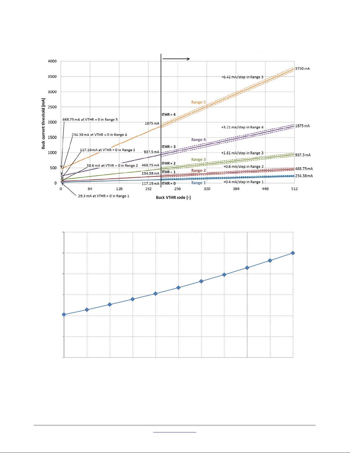
ITHR1_000 [BUCKx_VTHR = 000000000]
end of the BUCK ON−phase
ITHR1_219 [BUCKx_VTHR = 011011011]
end of the BUCK ON−phase
Min. value for specified precision
ITHR1_511 [BUCKx_VTHR = 111111111]
end of the BUCK ON−phase
ITHR2_000 [BUCKx_VTHR = 000000000]
end of the BUCK ON−phase
23.40 29.30 35.20 mA
117.19 mA
234.38 mA
46.90 58.59 70.30 mA
www.onsemi.com
10
Page 11

NCV78825
Table 12. BUCK REGULATOR – CURRENT REGULATION (continued)
Characteristic UnitMaxTypMinConditionsSymbol
Current Sense Threshold
Level, Range 2, Spec. Value
Current Sense Threshold
Level, Range 2, Max Value
Current Sense Threshold
Level, Range 3, Min Value
Current Sense Threshold
Level, Range 3, Spec. Value
Current Sense Threshold
Level, Range 3, Max Value
Current Sense Threshold
Level, Range 4, Min Value
Current Sense Threshold
Level, Range 4, Spec. Value
Current Sense Threshold
Level, Range 4, Max Value
Current Sense Threshold
Level, Range 5, Min Value
Current Sense Threshold
Level, Range 5, Spec. Value
Current Sense Threshold
Level, Range 5, Max Value
Current Sense Threshold
Increase per Code, Range 1
Current Sense Threshold
Increase per Code, Range 2
Current Sense Threshold
Increase per Code, Range 3
Current Sense Threshold
Increase per Code, Range 4
Current Sense Threshold
Increase per Code, Range 5
Current Threshold Accuracy
Only with Trimming Constant
for Range 5 (Note 23)
Current Threshold Accuracy
without Temperature
Compensation (Note 23)
Current Threshold Accuracy
(Note 23)
Offset of Peak Current
Comparator
Over−current Detection
Level, Range1
Over−current Detection
Level, Range2
Over−current Detection
Level, Range3
ITHR2_219
ITHR2_511 [BUCKx_VTHR = 111111111]
ITHR3_000 [BUCKx_VTHR = 000000000]
ITHR3_219 [BUCKx_VTHR = 011011011]
ITHR3_511 [BUCKx_VTHR = 111111111]
ITHR4_000 [BUCKx_VTHR = 000000000]
ITHR4_219 [BUCKx_VTHR = 011011011]
ITHR4_511 [BUCKx_VTHR = 111111111]
ITHR5_000 [BUCKx_VTHR = 000000000]
ITHR5_219
ITHR5_511 [BUCKx_VTHR = 111111111]
dITHR1
dITHR2
dITHR3
dITHR4
dITHR5
ITHR_ERR_DD Specified for BUCKx_VTHR
ITHR_ERR_D Specified for BUCKx_VTHR
ITHR_ERR
CMP_OFFSET BUCKx_OFF_CMP_DIS = 1 −10 +10 mV
OCDR1 305 mA
OCDR2 609 mA
OCDR3 1219 mA
[BUCKx_VTHR = 011011011]
end of the BUCK ON−phase.
Min. value for specified precision
end of the BUCK ON−phase
end of the BUCK ON−phase
end of the BUCK ON−phase
Min. value for specified precision
end of the BUCK ON−phase
end of the BUCK ON−phase
end of the BUCK ON−phase
Min. value for specified precision
end of the BUCK ON−phase
end of the BUCK ON−phase
[BUCKx_VTHR = 011011011]
end of the BUCK ON−phase
Min. value for specified precision
end of the BUCK ON−phase
9 bit, linear increase 0.40 mA
9 bit, linear increase 0.80 mA
9 bit, linear increase 1.61 mA
9 bit, linear increase 3.21 mA
9 bit, linear increase 6.42 mA
011011011, without the delta of
the trimming code and without
temp. compensation
011011011, with the delta of the
trimming code and without temp.
compensation
Specified for BUCKx_VTHR
011011011, the delta of the
trimming code and temp.
compensation
234.38 mA
468.75 mA
93.80 117.19 140.60 mA
468.75 mA
937.5 mA
187.50 234.38 281.30 mA
937.5 mA
1875 mA
375.00 468.75 562.50 mA
1875 mA
3750 mA
−9 +9 %
−7 +7 %
−4 +4 %
www.onsemi.com
11
Page 12

NCV78825
Table 12. BUCK REGULATOR – CURRENT REGULATION (continued)
Characteristic UnitMaxTypMinConditionsSymbol
Over−current Detection
Level, Range4
Over−current Detection
Level, Range5
Time Constant for Longest
Off Time
Time Constant for Shortest
Off Time
TOFF Time Relative Error
with Temperature
Compensation
TOFF Time Relative Error TOFF_ERR TC = Toff × VCOIL @ VLED > 2
TOFF Time Absolute Error TOFF_ERR_ABS TC = Toff × VCOIL @ VLED > 2
Time Constant Decrease per
Code
Detection Level of VLED to
be too Low
Zero−cross−detection
Threshold Level
Zero−cross−detection Filter
Time
HS Overvoltage Detection
Threshold Level
HS Overvoltage Detection
Filter Time
HS Gate Voltage Detection
Threshold Level
HS Gate Voltage Detection
Filter Time
OpenLEDx Detection Time TON_OPEN 40 50 60
Buck Minimum TON Time TON_MIN For
Delay from BUCKx ISENS
Comparator Input Voltage
Balance to BUCKx Switch
Going OFF
1. Measured as comparator DC threshold value, without comparator delay and switch falling slope.
OCDR4 2437 mA
OCDR5 4875 mA
TC_00 [BUCKx_TOFF = 00000] 50
TC_31 [BUCKx_TOFF = 11111] 5
TOFF_ERRW TC = Toff × VCOIL @ VLED > 2
Toff > 350 ns, Toff temperature
dependency relative to Thot =
155°C, see Figure 8
dTC
VLED_LMT 1.62 1.8 1.98 V
TC_ZCD −2.8 −1.2 −0.2 mV
TC_ZCD_FT 20 80 ns
OVD_THR LBCKSWx−VINBCKx, rising
OVD_FT 100 ns
HSVT_THR 0.6 V
HSVT_FT 45 ns
ISENSCMP_DEL ISENS cmp. over−drive ramp >
5 bits, exponential decrease 7.16 %
VINBCKx – LBCKSWx < 2.4 V,
no failure at LBCKSWx pin
for Slope = 1.25 A/μs, @125°C
V,
V,
Toff > 350 ns
V,
Toff 350 ns
edge
1 mV/10 ns,
−10 +10 %
−15 +15 %
−35 +35 ns
100 200 mV
50 250 ns
45 ns
ms × V
ms × V
ms
Table 13. BUCK REGULATOR – LS SWITCH PRE−DRIVER
Characteristic
Top Switch Ron Ront 40
Bottom Switch Ron Ronb 8
The Pull Down Resistor LS_PUD 10
LS FET Gate Voltage Threshold Level LS_VT Comparator level for non−overlap
LS FET Gate Voltage Comparator
Propagation Delay
The Maximum Reverse Polarity Current LS_IREV LSx_IREV_NOCTRL = 1 300 mA
Symbol Conditions Min Typ Max Unit
0.4 V
control when LS−>off, HS−>on
LS_DEL 10 ns
www.onsemi.com
12
W
W
kW
Page 13

NCV78825
Table 13. BUCK REGULATOR – LS SWITCH PRE−DRIVER (continued)
Characteristic UnitMaxTypMinConditionsSymbol
The non−overlap Time LS−off to HS−on
1. The time from detection of the LS switch in off state (pre−driver voltage at LS_VT threshold), to start of switching HS on.
Table 14. 5 V TOLERANT DIGITAL INPUTS (SCLK, CSB, SDI, LEDCTRL1, LEDCTRL2, RSTB)
Characteristic
High−level Input Voltage VINHI 2 V
Low−level Input Voltage VINLO 0.8 V
Pull Resistance (Note 1) Rpull 40 160
LED PWM Propagation Delay (Note 2) BUCKx_SW_DEL Activation time of the BUCKx
Sampling Resolution LEDCTRL_SR 100 125 ns
RSTB Debouncer Time RSTB_DEB 100 200 ns
1. Pull down resistor (Rpd) for RSTB, LEDCTRLx, SDI and SCLK, pull up resistor (Rpu) for CSB to VDD.
2. Jitter is present due to the internal resynchronization.
LS_DT Adaptive: LSx_NO_MD[1:0] = 00
30 ns
(Note 1)
LS_FNO1 Adaptive: LSx_NO_MD[1:0] = 01 1 6.5
LS_FNO2 Fixed: LSx_NO_MD[1:0] = 10 2.5
LS_FNO3 Fixed: LSx_NO_MD[1:0] = 11 5
Symbol Conditions Min Typ Max Unit
4.4 5.5 6.95
switch from the LEDCTRLx pin
% of
Toff
kW
ms
Table 15. 5 V TOLERANT OPEN−DRAIN DIGITAL OUTPUT (SDO)
Characteristic
Low−voltage Output Voltage VOUTLO Iout = −10 mA (current flows into the pin) 0.4 V
Equivalent Output Resistance RDSON Lowside switch 10 40
SDO Pin Leakage Current SDO_ILEAK 2
SDO Pin Capacitance SDO_C 10 pF
CLK to SDO Propagation
Delay
Symbol Conditions Min Typ Max Unit
SDO_DL Low−side switch activation/deactivation time;
60 ns
@1 kΩ to 5 V, 100 pF to GND, for falling
edge V(SDO) goes below 0.5 V
Table 16. 3V DIGITAL INPUTS (TEST, TEST1, TEST2)
Characteristic
High−level Input Voltage VIN3HI 2.3 V
Low−level Input Voltage VIN3LO 0.8 V
Pull Resistance Rpd3 Pull−down resistance 60
Symbol Conditions Min Typ Max Unit
Table 17. SPI INTERFACE
Characteristic
CSB Setup Time t
CSB Hold Time t
SCLK Low Time t
SCLK High Time t
Data−in (DIN) Setup Time, Valid Data
before Rising Edge of CLK
Data−in (DIN) Hold Time, Hold Data after
Rising Edge of CLK
Output (DOUT) Disable Time (Note1) t
Output (DOUT) Valid (Note 1)
Output (DOUT) Valid (Note 2)
Symbol Conditions Min Typ Max Unit
CSS
CSH
WL
WH
t
DIS
t
V1→0
t
V0→1
SU
t
H
0.5 μs
0.25 μs
0.5 μs
0.5 μs
0.25 μs
0.275 μs
0.08 0.32 μs
0.32 μs
0.32 + t(RC) μs
W
mA
kW
www.onsemi.com
13
Page 14
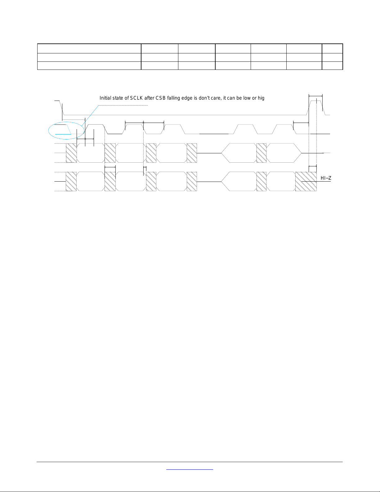
Table 17. SPI INTERFACE (continued)
t
Characteristic UnitMaxTypMinConditionsSymbol
Output (DOUT) Hold Time t
CSB High Time t
1. SDO low–side switch activation time
2. Time depends on the SDO load and pull–up resistor
HO
CS
NCV78825
0.01 μs
1 μs
V
IH
CSB
V
IL
V
IH
SCLK
V
IL
V
IH
DIN
V
IL
V
IH
DOUT
HI−Z
V
IL
Initial state of SCLK after CSB falling edge is don’t care, it can be low or high
t
CSS
SU
tHt
DIN15
t
V
t
WH
DIN14
t
WL
DIN13
t
HO
CSB
DIN1
DOUT15 DOUT14 DOUT13 DOUT1 DOUT0
Figure 5. SPI Communication Timing
DIN0
t
CSH
t
CS
DIS
HI−Z
www.onsemi.com
14
Page 15
TYPICAL CHARACTERISTICS
NCV78825
Accuracy (±4% / ±7% / ±9%) guaranteed from VTHR code 219 [dec]
219
Figure 6. Buck Peak Current vs. Ranges and VTHR Code
120
[%]
100
80
79,2
72,9
60
40
41,0
20
Buck Switch Rdson relative to value at 1605C
0
−40 −20 0 20 40 60 80 100 120 140 160
45,6
50,6
55,7
61,1
66,8
Temperature [5C]
85,9
100,0
92,7
Figure 7. Typical Temperature Behavior of Buck HS Switch Rdson Relative to the V alue at 160ºC
www.onsemi.com
15
Page 16

NCV78825
6
5
4
TOFF_err = −0.025 x Tj + 3.875
3
2
dependecy [%]
1
0
TOFF time relative error temperature
−45 −20 5 30 55 80 105 130 155
Temperature [5C]
Figure 8. TOFF Time Relative Error Temperature Dependency Relative to Thot at 155°C
75,0
70,0
65,0
60,0
55,0
50,0
45,0
Comparator delay [ns]
40,0
35,0
30,0
25,0
0,1 1 10
Slope [A/ms] for Range 5 (Note *)
Figure 9. Typical Comparator Delay vs Slope
1. Range 5: Comp. delay [ns] = (0.04 × Temp [ °C] + 40) × Slope [A/us, range 5] ^ (−0.17)
Notes:
2. Range 4: Comp. delay [ns] = (0.04 × Temp [ °C] + 40) × Slope × 2 [A/us, range 5] ^ (−0.17)
3. Range 3: Comp. delay [ns] = (0.04 × Temp [ °C] + 40) × Slope × 4 [A/us, range 5] ^ (−0.17)
4. Range 2: Comp. delay [ns] = (0.04 × Temp [ °C] + 40) × Slope × 8 [A/us, range 5] ^ (−0.17)
5. Range 1: Comp. delay [ns] = (0.04 × Temp [ °C] + 40) × Slope × 16 [A/us, range 5] ^ (−0.17)
*in lower ranges, the same current slope (A/μs) translates into a higher voltage slope (V/μs) at the input of the comparator,
because of the higher Rdson. Resulting equations for all ranges:
−40degC
25degC
85degC
125degC
150degC
www.onsemi.com
16
Page 17

NCV78825
DETAILED OPERATING DESCRIPTION
Supply Concept in General
Two voltages have to be brought to the NCV78825 chip
– low voltage VDRIVE supply and high voltage VBOOST
for providing energy to the buck regulators. More detailed
description follows.
VDRIVE Supply
The VDRIVE supply voltage represents power for the
complete LS pre−driver block as well as for VDD supply.
The selection of external LS FET is driven by available
voltage for VDRIVE supply. There is not implemented any
voltage monitor on VDRIVE supply.
VBOOSTM3V Supply
The VBOOSTM3V is the high side auxiliary supply for
driving the gates of the buck regulator’s integrated
high−side P−MOSFET switches. This supply receives
energy directly from the VBOOST pin, which has to be
connected by low impedance track to input pins of both buck
channels VINBCKx.
The dedicated Power−On−Reset circuit (POR) of
high−side P−MOSFET switches monitors correct voltage
level of both this auxiliary supply and VBOOST voltage in
order to guarantee correct control of integrated switches.
VDD Supply
The VDD supply is the low voltage digital and analog
supply for the chip and derives energy from VDRIVE supply
voltage. NCV78825 contains internal VDD regulator.
The Power−On−Reset circuit (POR) monitors the VDD
voltage and RSTB pin to control the out−of−reset and reset
entering state. At power−up, the chip will exit from reset
state when VDD > POR3V_H and RSTB pin is in “log. 1”.
No SPI communication is possible in reset state.
VBOOST Supply
The VBOOST supply voltage is the main high voltage
supply for the chip. The voltage is supposed to be provided
by booster chip such as NCV78702/3 or NCV78763 in the
application. VINBCKx pins have to be connected by low
impedance track to this supply to ensure proper buck
performance.
The VBOOST voltage is monitored by under−voltage
comparator to check sufficient zapping voltage at VBOOST
pin during OTP programming operation.
Module Startup
A limited transient activation of the buck switch inside the
NCV78825 device can be measured at module startup, when
supply voltages VBOOST and VDRIVE rise for the first
time and voltage regulators VDD and M3V pass POR
thresholds.
In rare application cases a limited energy transfer to the
buck circuit, may build a voltage on the output capacitor
which reaching the LED voltage threshold, resulting in a
weak light output pulse. The pulse duration can be
suppressed by using slower VBOOST slope, smaller M3V
capacitor, bigger output capacitor value and VDRIVE
supply connection before VBOOST supply.
Internal Clock Generation – OSC10M
An internal RC clock named OSC10M is used to run all
the digital functions in the chip. The clock is trimmed in the
factory prior to delivery. Its accuracy is guaranteed under
full operating conditions and is independent from external
component selection (refer to Table 9 for details). All
timings depend on OSC10M accuracy.
www.onsemi.com
17
Page 18

NCV78825
BUCK REGULATOR
General
The NCV78825 contains two high−current integrated
buck current regulators, which are the sources for the LED
strings. The bucks are powered from the external booster
regulator.
Buck Current Regulation Principle
Each buck controls the individual inductor peak current
(I
BUCKpeak
(ΔI
BUCKpkpk
current through the LED string, independently from the
string voltage. The buck average current is in fact described
by the formula:
This is graphically exemplified by Figure 10.
) and incorporates a constant ripple
) control circuit to ensure also stable average
DI
BUCK
I
BUCK
AVG
I
BUCK
peak
pkpk
2
(eq. 1)
The parameter I
BUCKpeak
is programmable through the
device by means of the internal registers for range selection
BUCKx_ISENS_THR[2:0] and current threshold code
BUCKx_VTHR[8:0]. The range setting will be applied only
after the setting of the current threshold in order to allow
smooth changes of peak current.
The formula that defines the total ripple current over the
buck inductor is also hereby reported:
(V
V
I
BUCK
pkpk
T
OFF
In the formula above, T
time, V
is the LED voltage feedback sensed at the
LED
LED
L
BUCK
OFF
NCV78825 VLEDx pin and L
value. The parameter T
OFF
× V
)
DIODE
T
represents the buck switch off
is the buck inductance
BUCK
is programmable by SPI
COIL
V
COIL
BUCK
(eq. 2)
off
L
(BUCKx_TOFF[4:0] register), with values related to Table
12. In order to achieve a constant ripple current value, the
device varies the T
V
sensed at the device pin, according to the selected
COIL
factor T
OFF
× V
COIL
time inversely proportional to the
OFF
.
As a consequence to the constant ripple control and
variable off time, the buck switching frequency depends on
the boost voltage and LED voltage in the following way:
Figure 10. Buck Regulator Controlled
Average Current
f
BUCK
(V
BOOST
V
V
BOOST
LED
)
T
If the offset cancelation of the peak current comparator is
not disabled by BUCKx_OFF_CMP_DIS bit, the inductor
Toff = constant
Toff = constant
Figure 11. Peak Current Comparator Offset Cancelation
The LED average current in time (DC) is equal to the buck
time average current. Therefore, to achieve a given LED
current target, it is sufficient to know the buck peak current
and the buck current ripple. A rule of thumb is to count a
minimum of 50% ripple reduction by means of the capacitor
C
and this is normally obtained with a low cost ceramic
BUCK
component ranging from 100 nF to 470 nF (such values are
1
OFF
(V
BOOST
V
V
BOOST
LED
V
)
COIL
T
V
off
COIL
peak current will vary from cycle−to−cycle as depicted on
Figure 11.
Toff = constant
Typical LED current
2x Peak current comparator offset
Fixed peak level
typically used at connector sides anyway, so this is included
in a standard BOM). The use of C
is a cost effective
BUCK
way to improve EMC performances without the need to
increase the value of L
, which would be certainly a far
BUCK
more expensive solution. The following figure reports a
typical example waveform:
(eq. 3)
www.onsemi.com
18
Page 19

NCV78825
Figure 12. LED Current AC Components Filtered out by Output Impedance (Oscilloscope Snapshot)
SW Compensation of the Buck Current Accuracy
In order to ensure buck current accuracy as specified in
Table 12, set of constants trimmed during manufacturing
process is available. Microcontroller should use them in the
following way:
To reach ±9 % accuracy (±7 % for Range 5) over whole
temperature operating range:
• All ranges: BUCKx_ISENS_TRIM[6:0] =
BUCKx_ISENS_RNG[6:0]
• BUCKx_ISENS_RNG[6:0] is trimming constant for
the highest current range (Range 5) at hot temperature
• BUCKx_ISENS_RNG[6:0] constant is loaded into
BUCKx_ISENS_TRIM[6:0] register automatically
after the reset of the device
To reach ±7 % accuracy over whole temperature operating
range:
• BUCKx_ISENS_Dx[3:0] registers, meaning delta of
the trimming constant with respect to the higher current
range at hot temperature, have to be used. Trimming
constant for the particular range at hot temperature can
be then calculated as:
• Range 5:
BUCKx_R5_trim_hot = BUCKx_ISENS_RNG[6:0],
• Range 4:
BUCKx_R4_trim_hot = BUCKx_ISENS_RNG[6:0]
+ BUCKx_ISENS_D4[3:0],
• Range 3:
BUCKx_R3_trim_hot = BUCKx_ISENS_RNG[6:0]
+ BUCKx_ISENS_D4[3:0] +
BUCKx_ISENS_D3[3:0],
• Range 2:
BUCKx_R2_trim_hot = BUCKx_ISENS_RNG[6:0]
+ BUCKx_ISENS_D4[3:0] +
BUCKx_ISENS_D3[3:0] +
BUCKx_ISENS_D2[3:0],
• Range 1:
BUCKx_R1_trim_hot = BUCKx_ISENS_RNG[6:0]
+ BUCKx_ISENS_D4[3:0] +
BUCKx_ISENS_D3[3:0] +
BUCKx_ISENS_D2[3:0] +
BUCKx_ISENS_D1[3:0],
Where delta of the trimming constant
BUCKx_ISENS_Dx[3:0] is signed, coded as two’s
complement. Range of this constant is decadic <−8; 7>,
binary <1000; 0111>.
Calculated trimming constant of selected range (y) has to
be then written into trimming SPI register:
BUCKx_ISENS_TRIM[6:0] = BUCKx_Ry_trim_hot
To reach ±4 % accuracy over whole temperature operating
range:
• In addition to BUCKx_ISENS_Dx[3:0] registers, the
BUCK_ISENS_TCx[3:0] registers, meaning
temperature coefficient for the appropriate range, have
to be used. Trimming value for a certain temperature
can be then calculated as:
• Range 5:
BUCK1_R5_trim = BUCK1_R5_trim_hot
× (Tj – Thot) + kQ × (Tj – Thot)2,
+ k
L1
BUCK2_R5_trim = BUCK2_R5_trim_hot
× (Tj – Thot) + kQ × (Tj – Thot)
+ k
L3
2
• Range 4:
BUCK1_R4_trim = BUCK1_R4_trim_hot
× (Tj – Thot) + kQ × (Tj – Thot)2,
+ k
L1
BUCK2_R4_trim = BUCK2_R4_trim_hot
× (Tj – Thot) + kQ × (Tj – Thot)
+ k
L3
2
• Range 3:
BUCK1_R3_trim = BUCK1_R3_trim_hot
× (Tj – Thot) + kQ × (Tj – Thot)2,
+ k
L1
BUCK2_R3_trim = BUCK2_R3_trim_hot
× (Tj – Thot) + kQ × (Tj – Thot)
+ k
L3
2
• Range 2:
BUCK1_R2_trim = BUCK1_R2_trim_hot
× (Tj – Thot) + kQ × (Tj – Thot)2,
+ k
L0
BUCK2_R2_trim = BUCK2_R2_trim_hot
× (Tj – Thot) + kQ × (Tj – Thot)2,
+ k
L2
• Range 1:
BUCK1_R1_trim = BUCK1_R1_trim_hot
× (Tj – Thot) + kQ × (Tj – Thot)2,
+ k
L0
BUCK2_R1_trim = BUCK2_R1_trim_hot
× (Tj – Thot) + kQ × (Tj – Thot)
+ k
L2
Where buck temperature coefficient
BUCK_ISENS_TCx[3:0] is signed, coded as two’s
complement. Range of this constant is decadic <−8; 7>,
binary <1000; 0111>
2
www.onsemi.com
19
Page 20

NCV78825
• k
is linear coefficient for each current range
Lx
calculated:
k
= (BUCK_ISENS_TCx[3:0] –
Lx
k
(200°C)2)/(−200°C) [code/°C]
Q x
• k
is quadratic constant for all current ranges:
Q
k
= 1.2 × 10
Q
−4
[code/(°C)2]
• Tj is junction temperature in °C calculated from
VTEMP[7:0] SPI register value according to the
equation defined in chapter ADC: Device Temperature
ADC: V
TEMP
• Thot temperature is constant equal to 155°C
Calculated trimming constant of selected range (y) has to
be then written into trimming SPI register:
VBOOST
supply
C
M3V
VBOOSTM3V VBOOST
VBOOSTM3V
reg.
BUCKx_ISENS_TRIM[6:0] = BUCKx_Ry_trim
The BUCKx_ISENS_TRIM[6:0] SPI register allows
compensation of the peak current app. in range ±40 % from
actual value according to the following equation:
IBUCKx = (ITHRx_000 +
δITHRx × BUCKx_VTHR[8:0]) × (1 + 0.4 × (
(BUCKx_ISENS_TRIM[6:0] − 63)/63)),
Where ITHRx_000 is current for VTHR code 0 in ITHRx
range (see Table 12), δITHRx code step in range ITHRx
(see Table 12).
The complete buck circuit diagram follows:
VINBCKx
POWER STAGE
Driver
HSVt
cmp
Digital
Control
Zero Cross Detector
Isense/OC /
OVD
Constant Ripple
Control
Figure 13. Buck Regulator Circuit Diagram
The zero−cross−detection (ZCD) comparator is
implemented for the case when VLED is low (< 1.8 V typ.)
to ensure proper Toff time termination just at the moment
when the coil current decreases to zero (boundary
conduction mode).
LBCKSWx
ZCD
LSFETx
GNDSx
VLEDx
L
M
Dbulk
LED string
C
ZCD is also used in normal buck mode when LS switch is
functional for proper determination of LS switch activation
and also deactivation when LS switch should be disabled in
reverse buck current mode.
www.onsemi.com
20
Page 21

NCV78825
HSVt Comparator
The HSVt comparator senses the gate voltage of the HS
switch and is used together with ZCD comparator for proper
activation of the LS switch. The comparator indicates that
gate voltage of the HS switch is at its Vt voltage, so it is safe
to turn LS switch on without risk of cross−current from
VBOOST/VINBCKx to ground.
Over Current Protection
Being a current regulator, the NCV78825 buck is by
nature preventing overcurrent in all normal situations.
However, in order to protect the system from overcurrent
even in case of failures, protection mechanism is available.
This protection is based on internal sensing over the buck
switch: when the peak current rises above the limit (situated
above OCDRx level, see Table 12), an internal counter starts
to increment at each period, until the count written in
BUCK_OC_OCCMP_THR[1:0] + 1 is attained. The
counter is reset if the buck channel is disabled and also at
each dimming cycle. From the moment the count is reached
onwards, the buck is kept continuously off, until the SPI
error flag OCLEDx is read. After reading the flag, the buck
channel “x” is automatically re−enabled and will try to
regulate the current again.
Over Voltage Detector
The OVD comparator ensures switching ON the HS
switch in case, that LBCKSWx pin is externally overdriven
over the VINBCKx potential. This feature prevents possible
HS switch bulk current and associated power loss or even
latch−up.
LS pre−driver
The LS pre−driver drives external NMOS device that is
performing synchronous rectification. The main advantage
is more efficient buck performance by minimizing voltage
drop across the flyback diode. The pre−driver is supplied
from VDRIVE pin, so its output is either switched to
VDRIVE or to GNDSx based on the required state of the LS
switch.
Implemented pull−down resistor ensures off state of the
LS switch in case that there is no supply of the device.
The LS pre−driver also contains the output voltage
monitor, the comparator indicating that LS switch gate
voltage is below a certain threshold voltage. The switching
on of the LS driver (LS pre−driver output is switched to
VDRIVE) is in normal continuous buck mode determined
by ZCD or HSVt comparator, the faster event activates the
LS switch.
The different buck modes and corresponding LS switch
functionality is implemented as follows:
• Buck output current discontinuous mode,
(VLED>VLED_LMT, LSx_IREV_NOCTRL = 0) the
LS driver is switched off as soon as the voltage drop
across the LS switch rises above ZCD threshold and
stays off till end of the corresponding Toff period
• Buck output current discontinuous mode,
(VLED>VLED_LMT, LSx_IREV_NOCTRL = 1) the
LS driver stays on till end of the Toff period regardless
of the ZCD state. The maximum buck output reverse
current (LS_IREV) is not sensed by the chip. It is
responsibility of application to guarantee that the
current will never exceed the specified value
• VLED_LOW is active,
(VLED<VLED_LMT, LSx_VLEDLOW_ENA = 0) the
LS driver is deactivated immediately, the bulk diode of
the LS switch is working as a flyback diode
• VLED_LOW is active,
(VLED<VLED_LMT, LSx_VLEDLOW_ENA = 1) the
LS driver stays functional like in case of high VLED
voltage (VLED>VLED_LMT)
• LS driver is disabled (LSx_DRV_ENA = 0), the LS
pre−driver output is switched to GNDSx, the LS switch
is kept off
Non−overlap Control of HS and LS Switches
The Non−overlap time is controlled in such a way, that HS
switch is activated just at the moment when gate voltage of
the LS switch is below its threshold voltage still with some
safety non−overlap time (see Table 13 for details). The
different non−overlap times can be selected by LS
non−overlap mode selection SPI bits:
• Adaptive mode (LSx_NO_MD[1:0] = “00” or “01”),
the switching off of the LS driver and switching on of
the HS driver is controlled by the self−adaptation
circuitry. This circuitry ensures, that the HS switch is
switched on just at the moment when gate voltage of
the LS FET passes through a LS_VT threshold when
the LS FET is surely off.
During settling time, the LS FET can be switched off
earlier than in balanced state, but the LS FET on time is
corrected for the next buck period in such a way, that
the balanced state should be reached.
During settling time, the LS FET can be switched off
later than in balanced state, but the LS FET on time is
corrected for the next buck period in such a way, that
the balanced state should be reached. As a
consequence, the Toff time must be extended just for
this buck period to prevent the cross−current
• Fixed mode (LSx_NO_MD[1:0] = “10” or “11”), the
switching off of the LS driver and switching on of the
HS driver is controlled by constant time as fixed
percentage of Toff time regardless of the LS FET
parasitics and switch−off time. In case of improper
application setup, the fixed non−overlap time can be too
short for given Toff time. In such case Toff time is
automatically extended just to prevent cross−current
(LS switch is still on, but HS switch should be already
switched on)
www.onsemi.com
21
Page 22

LBCKSW
I
COIL
HSVt_CMP
ZCD
HS_ON
LS_ON
NCV78825
T
OFF
LS_vt
Figure 14. Adaptive HS/LS Non-overlap Control
Paralleling the Bucks for Higher Current Capability
Different buck channels can be paralleled at the module
output (after the buck inductors) for higher current
capability on a unique channel, summing up together the
individual DC currents.
The Buck channels can be configured to a master−slave
synchronization mode by SPI bit BUCK_SYNC set to “1”.
Then, the Buck 1 performs as in the normal mode, the
Buck 2 “ON” phase starts when Buck1 “ON” phase finishes
(Buck 1 peak current reached) and also Buck 2 “OFF” phase
is synchronized with this signal from the master (Buck 2
Toff generator is not used). Only adaptive non−overlap
control for Buck 2 is allowed (LS2_NO_MD[1:0] = “00” or
“01”). If fixed non−overlap is set (LS2_NO_MD[1:0] =
“10” or “11”) then LS2_NO_MD[1:0] = “01” is set in the
device automatically. The duty cycle has to be less than 50%
for proper synchronous operation. This mode of operation is
suitable for further improvement of EMC performance, but
for the cost of worse Buck 2 average current accuracy.
Dimming
The NCV78825 supports both analog and digital
dimming (or so called PWM dimming). Analog dimming is
performed by controlling the LED amplitude current during
operation. This can be done by means of changing the peak
current level and/or the T
OFF
× V
constants by SPI
COIL
commands (see Buck Regulator section).
In this section, only the PWM dimming is described as this
is the preferred method to maintain the desired LED color
temperature for a given current rating. In PWM dimming,
the LED current waveform frequency is constant and the
duty cycle is set according to the required light intensity. In
Wait for LS_vt – Toff extended
order to avoid the beats effect, the dimming frequency
should be set at “high enough” values, typically above
300 Hz.
PWM dimming is controlled externally by means of
LEDCTRLx inputs.
External Dimming
The two independent control inputs LEDCTRLx handle
the dimming signals for the related channel “x”. In external
dimming, the buck activation is transparently linked to the
logic status of the LEDCTRLx pins. The only difference is
the controlled phase shift of typical 5.5 μs (see
BUCKx_SW_DEL parameter in Table 14) that allows
synchronized measurements of the VLEDx pins via the
ADC (see dedicated section for more details). As the phase
shift is applied both to rising edges and falling edges, with
a very limited jitter, the PWM duty cycle is not affected.
Apart from the phase shift and the system clock OSC10M,
there is no limitation to the PWM duty cycle values or
resolutions at the bucks, which is a copy of the reference
provided at the inputs.
ZOOM: buck inductor switching current
DIM_DUT = DIM_TON / DIM_T = DIM_T
DIM_T
ON
DIM_T
Figure 15. Buck Current Digital or PWM Dimming
ON
x F
www.onsemi.com
22
Page 23

NCV78825
ADC
General
The built−in analog to digital converter (ADC) is an 8−bit
capacitor based successive approximation register (SAR).
This embedded peripheral can be used to provide the
following measurements to the external Micro Controller
Unit (MCU):
• VBOOST voltage: sampled at the VBOOST pin
• VDD voltage: sampled at the VDD pin
• VLED1ON, VLED2ON voltages
• VLED1 and VLED2 voltages
• VTEMP measurement (chip temperature)
The internal NCV78825 ADC state machine samples all
the above channels automatically, taking care for setting the
analog MUX and storing the converted values in memory.
The external MCU can readout all ADC measured values via
the SPI interface, in order to take application specific
decisions. Please note that none of the MCU SPI commands
interfere with the internal ADC state machine sample and
conversion operations: the MCU will always get the last
available data at the moment of the register read.
VDDsample & convert
V
sample & convert
BOOST
Update LED_SEL_DUR count;
When counter ripples, trigger
VLEDx interrupt for once
V
sample & convert
TEMP
V
sample & convert
BOOST
points marked with a rhombus, with a minimum cadence
corresponding to the number of the elapsed ADC sequences
(forced interrupt). In formulas:
T
VLEDx_INT_forced
LED_SEL_DUR[8 : 0] T
ADC_SEQ
(eq. 4)
In general, prior to the forced interrupt status, the
VLEDxON ADC interrupts are generated when a falling
edge on the control line for the buck channel “x” is detected
by the device. In case of external dimming, this interrupt
start signal corresponds to the LEDCTRLx falling edge
together with a controlled phase delay (Table 14). The
purpose of the phase delay is to allow completion the
ongoing ADC conversion before starting the one linked to
the VLEDx interrupt: if at the moment of the conversion
LEDCTRLx pin is logic high, then the updated registers are
VLEDxON[7:0] and VLEDx[7:0]; otherwise, if
LEDCTRLx pin is logic low, the only register refreshed is
VLEDx[7:0]. This mechanism is handled automatically by
the NCV78825 logic without need of intervention from the
user, thus drastically reducing the MCU cycles and
embedded firmware and CPU cycles overhead that would be
otherwise required.
To avoid loss of data linked to the ADC main sequence,
one LED channel is served at a time also when interrupt
requests from both channels are received in a row and a full
sequence is required to go through to enable a new interrupt
VLEDx. In addition, possible conflicts are solved by using
a defined priority (channel pre−selection). Out of reset, the
default selection is given to channel “1”. Then an internal
flag keeps priority tracking, toggling at each time between
channels pre−selection. Therefore, up to two dimming
periods will b e required to obtain a full measurement update
of the two channels. This is not considered however a
limitation, as typical periods for dimming signals are in the
order of 1 ms period, thus allowing very fast failure
detection.
A flow chart referring to the ADC interrupts is also
displayed (see Figure 17).
Figure 16. ADC Sample and Conversion
Main Sequence
Referring to the figure above, the typical rate for a full
SAR plus digital conversion per channel is 8 μs (T able 10).
For instance, each new VBOOST ADC converted sample
occurs at 16 μs typical rate, whereas for both the VBB and
VTEMP channel the sampling rate is typically 32 μs, that is
to say a complete cycle of the depicted sequence. This time
is referred to as TADC_SEQ.
If the SPI setting LED_SEL_DUR[8:0] is not zero, then
interrupts for the VLEDx measurements are allowed at the
www.onsemi.com
23
Page 24

NCV78825
LEDx sample & convert
Toggle channel “x” selection
NO
Interrupts Enabled
NO
Proceed to next step in the
Figure 17. ADC VLEDx Interrupt Sequence
YES
V
second channel do not serve
immediately and complete
VLEDx
Synchronization
signal?
YES
In case of interrupt on
the ADC sequence first
ADC sequence
All NCV78825 ADC registers data integrity is protected
by ODD parity on the bit 8 (that is to say the 9th bit if
counting from the least significant bit named “0”). Please
refer to the SPI map section for further details.
Logic Supply Voltage ADC: V
DD
The logic supply voltage is sampled at VDD pin. The
(8−bit) conversion ratio is 4/255 (V/dec) = 0.0157 (V/dec)
typical. The converted value can be found in the SPI register
VDD[7:0], protected with ODD parity bit.
Boost Voltage ADC: V
BOOST
This measure refers to the boost voltage at the VBOOST
pin, with an 8 bit conversion ratio of 70/255 (V/dec) = 0.274
(V/dec) typical, inside the SPI register VBOOST[7:0]. The
value is protected by ODD parity bit. This measurement can
be used by the MCU for diagnostics and booster control loop
monitoring.
Device Temperature ADC: V
TEMP
By means of the VTEMP measurement, the MCU can
monitor the device junction temperature (T
) over time. The
J
conversion formula is:
TJ (VTEMP[7 : 0] 50.5)0.805
(eq. 5)
VTEMP[7:0] is the value read out directly from the
related 8bit−SPI register (please refer to the SPI map). The
value is also used internally by the device for the thermal
warning and thermal shutdown functions. More details on
these two can be found in the dedicated sections in this
document. The value is protected by ODD parity bit.
LED String Voltages ADC: V
LEDx
, V
LEDxON
The voltage at the pins VLEDx (1, 2) is measured. There
are 4 ranges available, that can be selected by means of
ADC_VLEDx_RNG_SEL[1:0] register, to obtain higher
resolution for LED voltage measurement.
Conversion ratios in dependency on selected range are:
0x0: 70/255 (V/dec) = 0.274 (V/dec)
0x1: 50/255 (V/dec) = 0.196 (V/dec)
0x2: 40/255 (V/dec) = 0.157 (V/dec)
0x3: 30/255 (V/dec) = 0.118 (V/dec)
This information, found in registers VLEDxON[7:0] and
VLEDx[7:0], can be used by the MCU to infer about the
LED string status, for example, individual shorted LEDs. As
for the other ADC registers, the values are protected by
ODD parity.
Please note that in the case of constant LEDCTRLx inputs
and no dimming (in other words dimming duty cycle equals
to 0% or 100%) the VLEDx interrupt is forced with a rate
equal to, given in the ADC general section. This feature can
be exploited by MCU embedded algorithm diagnostics to
read the LED channels voltage even when in OFF state,
before module outputs activation (module startup
pre−check).
www.onsemi.com
24
Page 25

NCV78825
DIAGNOSTICS
The NCV78825 features a wide range of embedded
diagnostic features. Their description follows. Please also
refer to the previous SPI section for more details.
w Thermal Warning:
This mechanism detects a user−programmable junction
temperature which is in principle close, but lower, to
the chip maximum allowed, thus providing the
information that some action (power de−rating) is
required to prevent overheating that would cause
Thermal Shutdown. A typical power de−rating
technique consists in reducing the output dimming duty
cycle in function of the temperature: the higher the
temperature above the thermal warning, the lower the
duty cycle. The thermal warning flag (TW) is given in
status register 0x16 and is latched. When VTEMP[7:0]
raises to or above THERMAL_WARNING_THR[7:0]
threshold, the TW flag is set. At power up the default
thermal warning threshold is typically 159°C (SPI code
179)
w Thermal Shutdown:
This safety mechanism intends to protect the device
from damage caused by overheating, by disabling the
both buck channels. The diagnostic is displayed per
means of the TSD bit in status register 0x16 (latched).
Once occurred, the thermal shutdown condition is
exited when the temperature drops below the thermal
warning level, thus providing hysteresis for thermal
shutdown recovery process. Outputs are re−enabled
automatically if BUCKx_TSD_AUT_RCRV_EN = 1,
respectively can be re−enabled by rising edge on
BUCKx_EN if BUCKx_TSD_AUT_RCRV_EN = 0.
The application thermal design should be made as such
to avoid the thermal shutdown in the worst case
conditions. The thermal shutdown level is not user
programmable and is factory trimmed (see ADC_TSD
in Table 10)
w SPI Error:
In case of SPI communication errors the SPIERR bit in
status register 0x16 is set. The bit is latched. For more
details, please refer to section “SPI protocol: framing
and parity error”
w Open LEDx String:
Individual open LED diagnostic flags indicate whether
the “x” string is detected open. The detection is based
on a counter overflow of typical 50 μs when the related
channel is activated. Both OPENLED1 and
OPENLED2 flags (latched) are contained in status
register 0x15. Please note that the open detection does
not disable the buck channel(s)
w Short LEDx String:
A short circuit detection is available independently for
each LED channel per means of the flag SHORTLEDx
(latched, status register 0x15). The detection is based
on the voltage measured at the VLEDx pins via a
dedicated internal comparator: when the voltage drops
below the VLED_LMT threshold (1.8 V typ. , see
Table 11) the related flag is set. Note that the detection
is active when buck channel is enabled and inactive
during the 1
of low VLEDx voltage the Toff time is terminated
immediately when the inductor current reaches zero.
This improves the dimming behavior via external short
switches (pixel control)
st
switching period after enabling. In case
w Overcurrent on Channel x:
This diagnostics protects the LEDx and the buck
channel x electronics from overcurrent. As the
overcurrent is detected, the OCLEDx flag (latched,
status register 0x15) is raised and the related buck
channel is disabled. More details about the detection
mechanisms and parameters are given in section “Buck
Overcurrent Protection”
w Buckx Status:
Register BUCKx_STATUS shows the actual status of
Buckx output. When BUCKx_STATUS is 1, the
corresponding output regulates current to the LED
w LEDCTRLx Pin Status:
SPI registers LED1VAL resp. LED2VAL indicate the
actual logic level of the debounced LEDCTRLx pins.
These signals follow the output of 200 ns digital
debouncers implemented on LEDCTRLx pins
w Buckx Running at Minimum TON Time:
Register BUCKx_MIN_TON (latched) indicates that
minimal TON time is detected on the corresponding
channel. It is clear by read flag. This information can be
used for detection of transition period during which the
BUCKx output current decreases due to the change of
BUCKx_VTHR code or BUCKx_ISENS_THR range
w Buckx TON Time Duration:
SPI register BUCKx_TON_DUR[7:0] reflects the last
measured Buckx TON time (1LSB = 200 ns) on the
corresponding channel. When Buckx runs with TON
time < typ. 200 ns, the BUCKx_TON_DUR[7:0] SPI
register returns value 0x00. When Buckx is stopped, the
BUCKx_TON_DUR[7:0] register keeps the last
measured TON time
w HW Reset:
The out of reset condition is reported through the HWR
bit (latched). This bit is set only at each Power On
Reset (POR) and indicates the device is ready to
operate
Each diagnostic latched flag is cleared by read.
A short summary table of the main diagnostic bits related
to the LED outputs follows.
www.onsemi.com
25
Page 26

NCV78825
Table 18. LED OUTPUTS DIAGNOSTIC SUMMARY
Diagnose
Flag Description
TW Thermal Warning SPI register programmable Not Disabled
TSD Thermal Shutdown Factory trimmed Disabled (automatically re−enabled
SPIERR SPI error See SPI section Not Disabled Yes
OPENLEDx LED string open circuit Buck on time > TON_OPEN Not Disabled Yes
SHORTLEDx LED string short circuit VLEDx < VLED_LMT Not Disabled Yes
OCLEDx LED string overcurrent Ibuckx > OCDR{1..5} Disabled Yes
Transition priority:
(0) − highest
(1)
(2)
(3) − lowest
Detection level LED Output Latched
(if no TSD, otherwise disabled)
when temp falls below TW and
BUCKx_TSD_AUT_RCVR_EN = 1)
Mode = RESET (0)
OFF
LED is off
TSD = 1 (1)
Yes
Yes
OCLEDx = 1 or
BUCKx_EN = 0 (2)
BUCKx_TSD_AUT_RCVR_EN = 1 or
rising edge on BUCKx_EN detected) (3)
BUCKx_TSD_AUT_RCVR_EN = 1 or
rising edge on BUCKx_EN detected) and
(OCLEDx = 1 or BUCKx_EN = 0) (2)
OCLEDx = 0 and
BUCKx_EN = 1 (2)
NORMAL mode: LED is on if LEDCTRLx = 1
FSO/STANDALONE mode: LED is on
RECOVERY
LED is off
VTEMP < THERMAL EARNING_THR (1)
DIMMING
TSD = 1 (1)
TSD = 1 (1)
TSD
LED is off
Figure 18. LED Dimming State Diagram
www.onsemi.com
26
Page 27

FUNCTIONAL MODE DESCRIPTION
Transition condition (priority level):
action executed when transition is performed
(0) − highest
(1)
(2)
(3) − lowest
NCV78825
POR (0)
RESET
SPI disabled
Dimming disabled
HWR := 1
RSTB = 0 and
(FSO_MD = 000 or
001 or 110 or 111) (1)
RSTB = 1 (1)
150μs timeout expired (3)
SPI pre−load from OTPs when
FSO_MD = 001 or 100 or 101
RSTB = 0 and
(FSO_MD = 010 or
011 or 100 or 101) and
OTP_CUST_LOCK = 1 (2)
SPI pre−load from OTPs
FSO := 1
INIT
SPI disabled
Dimming disabled
OTP refresh ongoing
150μs timeout expired
(
FSO_MD = 110 or111) and
OTP_CUST_LOCK = 1 (2)
SPI pre−load from OTPs
NORMAL
SPI enabled
Dimming: LEDCTRLx
(FSO_MD = 000 or 001) (1)
RSTB = 0 (1)
FSO := 1
FSO_MD = 000 or 001 (2)
RSTB = 1 or
RSTB = 0 (1)
STANDALONE
SPI disabled when
FSO_MD = 110
Dimming: BUCKx_EN
FSO
SPI disabled when
FSO_MD = 010 or 100
Dimming: BUCKx_EN
Figure 19. Functional Modes State Diagram
Reset
Asynchronous reset is caused either by POR (POR always
causes asynchronous reset − transition to reset state) or by
falling edge on RSTB pin (in normal/stand−alone mode,
when FSO_MD[2:0] = 000 or 001 or 110 or 111).
www.onsemi.com
Init and Normal mode
Normal mode is entered through Init state after internal
delay of 150 μs. In Init state, OTP refresh is performed. If
OTP bits for FSO_MD[2:0] register and OTP Lock Bit are
programmed, transition to FSO/SA mode is possible.
27
Page 28

NCV78825
e
RSTB in normal or stand−alone mode
FSO/Stand−Alone Mode
FSO (Fail−Safe Operation)/Stand−Alone modes can be
used for two main purposes:
• Default power−up operation of the chip (Stand−Alone
functionality without external microcontroller or
preloading of the registers with default content for
default operation before microcontroller starts sending
SPI commands for chip settings)
• Fail−Safe functionality (chip functionality definition in
fail−safe mode when the external microcontroller
functionality is not guaranteed)
FSO/stand−alone function is controlled according to
Table 19. Entrance into FSO/Stand−alone mode is possible
only after customer OTP zapping when OTP Lock Bit is set.
After FSO mode activation, the FSO bit in status register
is set. FSO register is cleared by read register.
When FSO/Stand−Alone mode is activated, content of the
following SPI registers is preloaded from OTP memory:
BUCK1_VTHR[8:1]
BUCK1_ISENS_THR[1:0]
BUCK2_VTHR[8:1]
BUCK2_ISENS_THR[1:0]
BUCK1_TOFF[4:0]
BUCK2_TOFF[4:0]
BUCK1_EN
BUCK2_EN
FSO_MD[2:0]
BUCK1_TSD_AUT_RCVR_EN
BUCK2_TSD_AUT_RCVR_EN
BUCK_OC_OCCMP_THR[1:0]
BUCKx_ISENS_TRIM[6:0] register is preloaded from
corresponding BUCKx_ISENS_RNG[6:0] register.
In FSO (entered via falling edge on RSTB pin) and
Stand−Alone modes, BUCK1_EN & BUCK2_EN are
controlled from SPI register map (SPI registers are updated
from OTP’s after entrance into these modes).
BUCK1_EN and BUCK2_EN are supposed to be set ‘1’
for the BUCKx operation in the FSO/stand−alone mode.
When control registers are pre−loaded from OTP’s after
POR and FSO mode is not entered (valid for FSO_MD[2:0]
= 100 or 101), BUCK1_EN and BUCK2_EN are kept
inactive (‘0’) until the first valid SPI operation is finished
(even in FSO mode) to avoid potential activation of buck
regulators immediately after POR (to prevent undefined
state of LEDCTRLx pins in case MCU leaves POR later than
NCV78825).
In FSO and Stand−Alone modes, the logic level at
LEDCTRLx pins is ignored and external PWM dimming
with LEDCTRLx pins is not available. The outputs can be
dimmed only by means of BUCKx_EN register.
Prior to entrance into FSO mode, low level on RSTB pin
always generates reset of digital. Falling edge on RSTB pin
may generate either entrance into FSO mode or reset in
dependency on FSO_MD[2:0] register value.
Once FSO mode is entered via falling edge on RSTB pin,
reset function of RSTB pin is blocked until FSO mode is
exited. FSO mode can be exited by the rising edge on RSTB
pin or by writing FSO_MD[2:0] = 000 or 001 (possible only
in FSO modes, where SPI control register update is allowed:
FSO_MD[2:0] = 011 or 101).
In stand−alone mode (FSO_MD[2:0] = 110 or 1 1 1), RSTB
has always reset functionality.
During entrance into FSO mode, value of FSO_MD[2:0]
SPI register (preloaded from OTP at power up only) is
latched into internal register and all FSO related functions
are then controlled according to it. The purpose is to avoid
the reset of the device when FSO mode is active and
FSO_MD[2:0] is changed to value corresponding to
stand−alone mode, where RSTB pin has reset functionality.
The internal register is cleared after POR or when FSO mode
is exited.
POR
(internal)
RSTB
POR
(internal)
RSTB
Normal mode (SPI possible)
Power−up
Possible OTP pre−load Possible OTP pre−load
RSTB in FSO mode
Normal mode (SPI possible)
Power−up
OTP pre−load OTP pre−load
Figure 20. RSTB Pin Functionality in Normal, Stand−alone and FSO Modes
www.onsemi.com
Normal mode (no SPI)
FSO mode
(SPI possible/no SPI)
28
Normal mode
Reset mod
FSO modeNormal mode
OTP pre−load
Page 29

NCV78825
Table 19. FSO MODES
FSO_MD[2:0]
000b = 0 FSO mode disabled, registers are loaded with safe value = 0x00h after POR, default
− After the reset, control registers are loaded with 0x00h value
− Entrance into FSO mode is not possible unless dedicated SPI write command to change FSO_MD[2:0] value is
sent
− RSTB pin has reset functionality
− LEDCTRLx pins are functional (buck enable/disable, external PWM dimming available)
001b = 1 FSO mode disabled, registers are loaded with data from OTP memory after POR
− After the reset, control registers are loaded with data stored in OTP memory (device’s OTP memory has to be
programmed, OTP Lock Bit has to be set). It reduces number of SPI transfers needed to configure the device
after the reset
− Entrance into FSO mode is not possible unless dedicated SPI write command to change FSO_MD[2:0] value is
sent
− RSTB pin has reset functionality
− LEDCTRLx pins are functional (buck enable/disable, external PWM dimming available)
010b = 2 FSO entered after falling edge on RSTB pin, registers are loaded with safe value = 0x00h except FSO_MD[2:0]
value after POR
− After FSO mode activation, control registers are loaded with data stored in OTP memory
− SPI register update (SPI write/read operation) in FSO mode is disabled (SPI write operation is blocked;
Diagnostig flags clearing of SPI registers is blocked; in case of invalid SPI frame, SPIERR flag is set)
− RSTB pin serves to enter/exit FSO mode
− LEDCTRLx pins are not functional (buck enable/disable only by means of BUCKx_EN SPI/OTP bits, external
PWM dimming not available)
011b = 3 FSO entered after falling edge on RSTB pin, registers are loaded with safe value = 0x00h except FSO_MD[2:0]
value after POR
− After FSO mode activation, control registers are loaded with data stored in OTP memory
− SPI register update (SPI write/read operation) in FSO mode is enabled
− FSO mode can be exited by writing FSO_MD[2:0] = 000 or 001
− RSTB pins serves to enter/exit FSO mode
− LEDCTRLx pins are not functional (buck enable/disable only by means of BUCKx_EN SPI/OTP bits, external
PWM dimming not available)
100b = 4 FSO entered after falling edge on RSTB pin, registers are loaded with data from OTP memory after POR
− After FSO mode activation, control registers are loaded with data stored in OTP memory
− SPI register update (SPI write/read operation) in FSO mode is disabled (SPI write operation is blocked;
Diagnostig flags clearing of SPI registers is blocked; in case of invalid SPI frame, SPIERR flag is set)
− RSTB pin serves to enter/exit FSO mode
− LEDCTRLx pins are not functional (buck enable/disable only by means of BUCKx_EN SPI/OTP bits, external
PWM dimming not available)
101b = 5 FSO entered after falling edge on RSTB pin, registers are loaded with data from OTP memory after POR
− After FSO mode activation, control registers are loaded with data stored in OTP memory
− SPI register update (SPI write/read operation) in FSO mode is enabled
− FSO mode can be exited by writing FSO_MD[2:0] = 000 or 001
− RSTB pin serves to enter/exit FSO mode
− LEDCTRLx pins are not functional (buck enable/disable only by means of BUCKx_EN SPI/OTP bits, external
PWM dimming not available)
110b = 6 SA (stand−alone)/FSO entered after POR (RSTB pin rising edge), registers are loaded with data from OTP memory
− After SA/FSO mode activation, control registers are loaded with data from OTP memory
− SPI register update (SPI write/read operation) in SA/FSO mode is disabled (SPI write operation is blocked;
Diagnostig flags clearing of SPI registers is blocked; in case of invalid SPI frame, SPIERR flag is set)
− RSTB pin has reset functionality
− LEDCTRLx pins are not functional (buck enable/disable only by means of BUCKx_EN SPI/OTP bits, external
PWM dimming not available)
111b = 7 SA (stand−alone)/FSO entered after POR (RSTB pin rising edge), registers are loaded with data from OTP memory
− After SA/FSO mode activation, control registers are loaded with data from OTP memory
− SPI register update (SPI write/read operation) in SA/FSO mode is enabled
− FSO mode can be exited by writing FSO_MD[2:0] = 000 or 001
− RSTB pin has reset functionality
− LEDCTRLx pins are not functional (buck enable/disable only by means of BUCKx_EN SPI/OTP bits, external
PWM dimming not available)
Description
www.onsemi.com
29
Page 30

NCV78825
High
T
SPI INTERFACE
General
The serial peripheral interface (SPI) is used to allow
an external microcontroller (MCU) to communicate
with the device. NCV78825 acts always as a slave and it
cannot initiate any transmission. The operation of the device
is configured and controlled by means of SPI registers,
which are observable for read and/or write from the master.
The NCV78825 SPI transfer size is 16 bits.
During an SPI transfer, the data is simultaneously
transmitted (shifted out serially) and received (shifted in
serially). A serial clock line (CLK) synchronizes shifting
and sampling of the information on the two serial data lines:
SDO and SDI. The SDO signal is the output from the Slave
(NCV78825), and the SDI signal is the output from the
Master.
A slave or chip select line (CSB) allows individual
selection of a slave SPI device in a time multiplexed
multiple−slave system.
The CSB line is active low. If an NCV78825 is not
selected, SDO is in high impedance state and it does not
interfere with SPI bus activities. Since the NCV78825
always clocks data out on the falling edge and samples data
in on rising edge of clock, the MCU SPI port must be
configured to match this operation.
The implemented SPI allows connection to multiple
slaves by means of star connection (CSB per slave) or by
means of daisy chain.
An SPI star connection requires a bus = (3 + N) total lines,
where N is the number of Slaves used, the SPI frame length
is 16 bits per communication.
NCV78825 dev#1
(SPI Slave)
NCV78825 dev#2
(SPI Slave)
NCV78825 dev#N
(SPI Slave)
MCU
(SPI Master)
CSB1
CSB2
Figure 21. SPI Star vs. Daisy Chain Connection
SPI Daisy Chain Mode
SPI daisy chain connection bus width is always four lines
independently on the number of slaves. However, the SPI
transfer frame length will be a multiple of the base frame
length so N × 16 bits per communication: the data will be
interpreted and read in by the devices at the moment the CSB
rises.
A diagram showing the data transfer between devices in
daisy chain connection is given further: CMDx represents
the 16−bit command frame on the data input line transmitted
by the Master, shifting via the chips’ shift registers through
the daisy chain. The chips interpret the command once the
chip select line rises.
The NCV78825 default power up communication mode
is “star”. In order to enable daisy chain mode, a multiple of
16 bits clock cycles must be sent to the devices. It is
recommended to keep SDI line low during this first SPI
frame. In order to come back to star mode the NOP register
(address 0x00) must be written with all ones, with the proper
MCU
(SPI Master)
MOSI
MISO SDO1
SDI2
SDO2
SDIN
NCV78825 dev#1
(SPI Slave)
NCV78825 dev#2
(SPI Slave)
NCV78825 dev#N
(SPI Slave)
data parity bit and parity framing bit: see SPI protocol for
details about parity and write operation.
COMMANDS IN THE SHIF
CSB
SCLK
DIN
DOUT
DIN
DOUT
DIN
DOUT
16
CYCLES
CMD1 CMD2 CMD3
1
1
X
2
2
3
3
CYCLES16CYCLES
CMD1
X X
X X X
Low
16
CMD2
CMD1
Figure 22. SPI Daisy Chain Data Shift Between
Slaves. The symbol ‘x’ Represents the Previous
Content of the SPI Shift Register Buffer
REGISTERS ARE
EXECUTED ON RISING
EDGE OF CSB
www.onsemi.com
30
Page 31

NCV78825
SPI Transfer Format
Two types of SPI commands (to SDI pin of NCV78825)
from the micro controller can be distinguished: “Write to a
control register” and “Read from register (control or
status)”.
CSB
C
SDI
SDO
SCLK
M
D
S
P
I
E
R
R
S
P
I
E
R
R
A3A2A
C
A3A2A1A
M
D
C
A
M
4
D
A0D
P
1
0
A3A2A1A
D7D6D5D4D3D2D1D
D
9
8
D7D6D5D4D3D2D1D
D9D
8
P0 1 1
P
0
The frame protocol for the write operation:
Write; CMD = ‘1’
High
Low
0
Low
0
HIGH−Z
B
L
L
U
C
1
K
O
C
T
E
D
2
T
E
S
W
D
D
1
Low
Previous SPI WRITE command
resp. “SPIERR + 0x000hex”
after POR or SPI Command
PARITY/FRAMING Error
Previous SPI READ command
& NCV78825 status bits resp.
“SPIERR
POR or SPI Command
PARITY/FRAMING Error
+ 0x000hex” after
P = not (CMD xor A3 xor A2 xor A1 xor A0 xor D9 xor D8 xor D7 xor D6 xor D5 xor D4 xor D3 xor D2 xor D1 xor D0)
Figure 23. SPI Write Frame
Referring to the previous picture, the write frame coming
from the master (into the SDI) is composed from the
following fields:
• Bit[15] (MSB): CMD bit = 1 for write operation
• Bits[14:11]: 4 bits WRITE ADDRESS field
• Bit[10]: frame parity bit. It is ODD parity formed by
the negated XOR of all other bits in the frame
• Bits[9:0]: 10 bit DATA to write
Device in the same time replies to the master (on the
• If the previous command was a read, the response
frame summarizes the address used and an overall
diagnostic check (copy of the main detected errors, see
Figure 23 and Figure 24 for details)
• In case of previous SPI error, only the MSB bit will be
1, followed by zeros
• After power−on−reset all bits are zero
If parity bit in the frame is wrong, device will not perform
command and <SPI> flag will be set.
SDO):
• If the previous command was a write and no SPI error
had occurred, a copy of the command, address and data
written fields
www.onsemi.com
31
Page 32

The frame protocol for the read operation:
s
CSB
C
A3A2A
SDI
SDO
A
M
4
D
S
B
P
U
I
C
E
K
R
O
R
C
1
L
L
T
E
E
S
D
D
D
2
1
Read; CMD = ‘0’
A
P
0
D8D7D6D5D4D3D
D
T
W
9
NCV78825
Low
Low
2
D1D
High
LED 1 = OPENLED1 or SHORTLED1
LED 2 = OPENLED2 or SHORTLED2
BUCKOC = OCLED1 or OCLED2
−> immediate value of STATUS BITS;
Dedicated SPI READ Command of the
STATUS Register has to be performed to
clear the value of read−by−clear STATUS bit
Low
Data from address A[4:0]
0
shall be returned
HIGH−Z
SCLK
P = not (CMD xor A4 xor A3 xor A2 xor A1 xor A0)
Figure 24. SPI Read Frame
Referring to the previous picture, the read frame coming
from the master (into the SDI) is composed from the
following fields:
• Bit[15] (MSB): CMD bit = 0 for read operation
• Bits[14:10]: 5 bits READ ADDRESS field
• Bit[10]: frame parity bit. It is ODD parity formed by
the negated XOR of all other bits in the frame
• Bits [8:0]: 9 bits zeroes field
Device in the same frame provides to the master (on the
SDO) data from the required address (in frame response),
thus achieving the lowest communication latency .
Low
SPI Framing and Parity Error
SPI communication framing error is detected by the
NCV78825 in the following situations:
• Not an integer multiple of 16 CLK pulses are received
during the active−low CSB signal
• LSB bits (8..0) of a read command are not all zero
• SPI parity errors, either on write or read operation
Once an SPI error occurs, the <SPI> flag can be reset only
by reading the status register in which it is contained (using
in the read frame the right communication parity bit).
www.onsemi.com
32
Page 33

SPI ADDRESS MAP
T able 20. NCV78825 SPI ADDRESS MAP
ADDR R/W bit9 bit8 bit7 bit6 bit5 bit4 bit3 bit2 bit1 bit0
0x00 NA NOP Register (Read/Write Operation Ignored)
0x01 R/W 0x0 BUCK1_VTHR[8:0]
0x02 R/W 0x0 BUCK2_VTHR[8:0]
0x03 R/W 0x0 LS1_VLEDLOW
0x04 R/W BUCK1_TOFF[4:0] BUCK2_TOFF[4:0]
0x05 R/W BUCK1_OFF
0x06 R/W BUCK_SYNC LS1_NO_MD[1:0] LS2_NO_MD[1:0] LS1_DRV_ENA LS2_DRV_ENA LS1_IREV_NOCTRL LS2_IREV_NOCTRL x_BANK_SEL
0x07 R/W BUCK1_TSD
0x08 R/W VTEMP_OFF_COMP
0x09 R/W VTEMP_OFF_COMP[2:0]* BUCK1_ISENS_TRIM[6:0]
0x0A R/W VTEMP_OFF_COMP[5:3]* BUCK2_ISENS_TRIM[6:0]
0x0B R/W ADC_VLED1_RNG_SEL[1:0] ADC_VLED2_RNG_SEL[1:0] OTP_BIAS_H OTP_BIAS_L OTP_ADDR[1:0] OTP_OPERATION[1:0]
0x0C R 0x0 ODD PARITY VLED1ON[7:0]
0x0D R 0x0 ODD PARITY VLED2ON[7:0]
0x0E R 0x0 ODD PARITY VLED1[7:0]
0x0F R 0x0 ODD PARITY VLED2[7:0]
0x10 R 0x0 ODD PARITY VTEMP[7:0]
0x11 R 0x0 ODD PARITY VBOOST[7:0]
0x12 R 0x0 ODD PARITY VDD[7:0]
0x13 R 0x0 ODD PARITY BUCK1_TON_DUR[7:0]
0x14 R 0x0 ODD PARITY BUCK2_TON_DUR[7:0]
0x15 R 0x0 ODD PARITY 0x0 OPENLED1 SHORTLED1 OCLED1 OPENLED2 SHORTLED2 OCLED2
0x16 R 0x0 ODD PARITY OTP_FAIL FSO HWR LED1VAL LED2VAL SPIERR TSD TW
0x17 R 0x0 ODD PARITY 0x0 OTP_ACTIVE BUCK1_MIN_TON BUCK2_MIN_TON BUCK1_STATUS BUCK2_STATUS
0x18 R 0x0 ODD PARITY 0x0 BUCKx_ISENS_RNG[6:0]
0x19 R 0x0 ODD PARITY BUCKx_ISENS_D2[3:0] BUCKx_ISENS_D1[3:0]
0x1A R 0x0 ODD PARITY BUCKx_ISENS_D4[3:0] BUCKx_ISENS_D3[3:0]
0x1B R 0x0 ODD PARITY BUCK_ISENS_TC1[3:0] BUCK_ISENS_TC0[3:0]
0x1C R 0x0 ODD PARITY BUCK_ISENS_TC3[3:0] BUCK_ISENS_TC2[3:0]
0x1D R 0x0 ODD PARITY 0x0 BUCK_ISENS_TC4[3:0]
0x1E R OTP_DATA[9:0]
0x1F R 0x0 REVID[8:0]
OTHER R 0x0
_CMP_DIS
_AUT_RCVR_EN
ODD PAR.*
BUCK2_OFF
_CMP_DIS
BUCK2_TSD
_AUT_RCVR_EN
_ENA
DRV_SLOW_EN BUCK_OC_OCCMP_THR[1:0] FSO_MD[2:0] BUCK1_EN BUCK2_EN
*Read only.
LS2_VLEDLOW
_ENA
BUCK1_ISENS_THR[2:0] BUCK2_ISENS_THR[2:0]
THERMAL_WARNING_THR[7:0]
LED_SEL_DUR[8:0]
www.onsemi.com
33
Page 34

SPI Register Details
T able 21. NOP REGISTER 0x00
NOP Register 0x00
Address Bit 9 Bit 8 Bit 7 Bit 6 Bit 5 Bit 4 Bit 3 Bit 2 Bit 1 Bit 0
0x00
Name NOP[9:0]
Reset 0 0 0 0 0 0 0 0 0 0
Access R/W R/W R/W R/W R/W R/W R/W R/W R/W R/W
1. NOP[9:0]: No Operation register. Always reads zero.
When SPI in daisy chain mode, writing all ones will force a change to SPI star mode.
T able 22. BUCK1 PEAK CURRENT SETTINGS REGISTER 0x01
BUCK1 Peak Current Settings Register 0x01
Address Bit 9 Bit 8 Bit 7 Bit 6 Bit 5 Bit 4 Bit 3 Bit 2 Bit 1 Bit 0
0x01
0x01 Access R/W R/W R/W R/W R/W R/W R/W R/W R/W R/W
1. BUCK1_VTHR[8:0] − Buck 1 Peak Current value settings.
Value Range1 Range 2 Range 3 Range 4 Range 5
0 29.30 mA 58.59 mA 117.19 mA 234.38 mA 468.75 mA
219 117.19 mA 234.38 mA 468.75 mA 937.5 mA 1875 mA
511 234.38 mA 468.75 mA 937.5 mA 1875 mA 3750 mA
Step 0.4 mA 0.8 mA 1.61 mA 3.21 mA 6.42 mA
2. Range selection is related to value written in BUCK1_ISENS_THR[2:0] bits.
Name 0 BUCK1_VTHR[8:0]
Reset 0 0, FSO 0, FSO 0, FSO 0, FSO 0, FSO 0, FSO 0, FSO 0, FSO 0
T able 23. BUCK 2 PEAK CURRENT SETTINGS REGISTER 0x02
BUCK 2 Peak Current Settings Register 0x02
Address Bit 9 Bit 8 Bit 7 Bit 6 Bit 5 Bit 4 Bit 3 Bit 2 Bit 1 Bit 0
0x02
Name 0 BUCK2_VTHR[8:0]
Reset 0 0, FSO 0,FSO 0,FSO 0, FSO 0, FSO 0, FSO 0, FSO 0, FSO 0
Access R/W R/W R/W R/W R/W R/W R/W R/W R/W R/W
1. BUCK2_VTHR[8:0] − Buck 2 Peak Current value settings.
Value Range1 Range 2 Range 3 Range 4 Range 5
0 29.30 mA 58.59 mA 117.19 mA 234.38 mA 468.75 mA
219 117.19 mA 234.38 mA 468.75 mA 937.5 mA 1875 mA
511 234.38 mA 468.75 mA 937.5 mA 1875 mA 3750 mA
Step 0.4 mA 0.8 mA 1.61 mA 3.21 mA 6.42 mA
2. Range selection is related to value written in BUCK2_ISENS_THR[2:0] bits.
T able 24. BUCK PEAK CURRENT RANGE SETTINGS REGISTER 0x03
BUCK Peak Current Range Settings Register 0x03
Address Bit 9 Bit 8 Bit 7 Bit 6 Bit 5 Bit 4 Bit 3 Bit 2 Bit 1 Bit 0
0x03
1. LS1_VLEDLOW_ENA
2. LS2_VLEDLOW_ENA
Name 0 0 LS1_VLEDLOW_ENALS2_VLEDLOW_E
NA
Reset 0 0 0 0 0 0, FSO 0, FSO 0 0, FSO 0, FSO
Access R/W R/W R/W R/W R/W R/W R/W R/W R/W R/W
BUCK1_ISENS_THR[2:0] BUCK2_ISENS_THR[2:0]
Buck 1 Low Side Pre−driver Enable bit for low VLED voltage (< 1.8 V typ.).
0: LS1 Pre−driver disabled for low VLED.
1: LS1 Pre−driver enabled for low VLED.
Buck 2 Low Side Pre−driver Enable bit for low VLED voltage (< 1.8 V typ.).
0: LS2 Pre−driver disabled for low VLED.
1: LS2 Pre−driver enabled for low VLED.
www.onsemi.com
34
Page 35

3. BUCK1_ISENS_THR[2:0]
Buck 1 Peak Current Range selection.
000: Range 1
001: Range 2
010: Range 3
011: Range 4
100: Range 5
The range setting will be applied only after the writing BUCK1 Peak Current value in BUCK1_VTHR[8:0] bits.
4. BUCK2_ISENS_THR[2:0]
Buck 2 Peak Current Range selection.
000: Range 1
001: Range 2
010: Range 3
011: Range 4
100: Range 5
The range setting will be applied only after the writing BUCK2 Peak Current value in BUCK2_VTHR[8:0] bits.
T able 25. BUCK TOFF SETTINGS REGISTER 0x04
BUCK TOFF Settings Register 0x04
Address Bit 9 Bit 8 Bit 7 Bit 6 Bit 5 Bit 4 Bit 3 Bit 2 Bit 1 Bit 0
0x04
1. BUCK1_TOFF[4:0] − Buck 1 T ime Constant settings (TOFF*VCOIL) for keeping inductor ripple current.
0: 50.0 μs.V 11: 22.1 μs.V 22: 9.75 μs.V
1: 46.4 μs.V 12: 20.5 μs.V 23: 9.05 μs.V
2: 43.1 μs.V 13: 19.0 μs.V 24: 8.41 μs.V
3: 40.0 μs.V 14: 17.7 μs.V 25: 7.8 μs.V
4: 37.1 μs.V 15: 16.4 μs.V 26: 7.25 μs.V
5: 34.5 μs.V 16: 15.2 μs.V 27: 6.73 μs.V
6: 32.0 μs.V 17: 14.1 μs.V 28: 6.25 μs.V
7: 29.7 μs.V 18: 13.1 μs.V 29: 5.80 μs.V
8: 27.6 μs.V 19: 12.2 μs.V 30: 5.38 μs.V
9: 25.6 μs.V 20: 11.3 μs.V 31: 5.00 μs.V
10: 23.8 μs.V 21: 10.5 μs.V
2. BUCK2_TOFF[4:0] − Buck 2 T ime Constant settings (TOFF*VCOIL) for keeping inductor ripple current.
0: 50.0 μs.V 11: 22.1 μs.V 22: 9.75 μs.V
1: 46.4 μs.V 12: 20.5 μs.V 23: 9.05 μs.V
2: 43.1 μs.V 13: 19.0 μs.V 24: 8.41 μs.V
3: 40.0 μs.V 14: 17.7 μs.V 25: 7.8 μs.V
4: 37.1 μs.V 15: 16.4 μs.V 26: 7.25 μs.V
5: 34.5 μs.V 16: 15.2 μs.V 27: 6.73 μs.V
6: 32.0 μs.V 17: 14.1 μs.V 28: 6.25 μs.V
7: 29.7 μs.V 18: 13.1 μs.V 29: 5.80 μs.V
8: 27.6 μs.V 19: 12.2 μs.V 30: 5.38 μs.V
9: 25.6 μs.V 20: 11.3 μs.V 31: 5.00 μs.V
10: 23.8 μs.V 21: 10.5 μs.V
Name BUCK1_TOFF[4:0] BUCK2_TOFF[4:0]
Reset 0, FSO 0, FSO 0, FSO 0, FSO 0, FSO 0, FSO 0, FSO 0, FSO 0, FSO 0, FSO
Access R/W R/W R/W R/W R/W R/W R/W R/W R/W R/W
T able 26. BUCK SETTINGS REGISTER 0x05
BUCK Settings Register 0x05
Address Bit 9 Bit 8 Bit 7 Bit 6 Bit 5 Bit 4 Bit 3 Bit 2 Bit 1 Bit 0
0x05
Name BUCK1_
OFF_C
MP_DIS
Reset 0 0 0 0, FSO 0, FSO 0, FSO 0, FSO 0, FSO 0, FSO 0, FSO
Access R/W R/W R/W R/W R/W R/W R/W R/W R/W R/W
BUCK2_
OFF_C
MP_DIS
DRV_
SLOW_
EN
BUCK_OC_OCCMP_
THR[1:0]
FSO_MD[2:0] BUCK1
_EN
1. BUCK1_OFF_CMP_DIS − Buck 1 Peak current Comparator Offset Cancellation function.
0: Offset compensation enabled
1: Offset compensation disabled
2. BUCK2_OFF_CMP_DIS − Buck 2 Peak current Comparator Offset Cancellation function.
0: Offset compensation enabled
1: Offset compensation disabled
3. DRV_SLOW_EN − High Side drivers slopes settings.
0: Normal slopes
1: Slow slopes
4. BUCK_OC_OCCMP_THR[1:0] − Over−current Detection Setting
00: Over−current must be valid for more than 1 switching period
01: Over−current must be valid for more than 2 switching period
10: Over−current must be valid for more than 3 switching period
11: Over−current must be valid for more than 4 switching period
www.onsemi.com
35
BUCK2
_EN
Page 36

5. FSO_MD[2:0] − Fail−Safe Operation / Stand−Alone mode selection (See Table 19 for details).
000: FSO mode disabled, Registers loaded with Safe values,
001: FSO mode disabled, Registers loaded from OTP memory
010: FSO mode enabled, Registers loaded with Safe values
011: FSO mode enabled, Registers loaded with Safe values, SPI update in FSO
100: FSO mode enabled, Registers loaded from OTP memory
101: FSO mode enabled, Registers loaded from OTP memory, SPI update in FSO
110: Stand−alone mode, Registers loaded from OTP memory
111: Stand−alone mode, Registers loaded from OTP memory, SPI update in FSO
6. BUCK1_EN − Buck Regulator Channel 1 Enable bit.
0: Buck 1 disabled
1: Buck 1 enabled
7. BUCK2_EN − Buck Regulator Channel 2 Enable bit.
0: Buck 2 disabled
1: Buck 1 enabled
T able 27. BUCK SETTINGS REGISTER 0x06
BUCK Settings Register 0x06
Address Bit 9 Bit 8 Bit 7 Bit 6 Bit 5 Bit 4 Bit 3 Bit 2 Bit 1 Bit 0
0x06
1. BUCK_SYNC − Activation of the Bucks synchronous operation.
0: Normal mode − Bucks synchronous operation Disabled
1: Master−slave mode − Bucks synchronous operation Enabled
2. LS1_NO_MD[1:0] − Buck 1 Low Side Pre−driver Non−overlap mode LS to HS selection.
00: Adaptive mode, 30 ns dead time
01: Adaptive mode, min 1% of TOFF time
10: Fixed mode, 2.5% of TOFF time
11: Fixed mode, 5% of T OFF time
3. LS2_NO_MD[1:0] − Buck 2 Low Side Pre−driver Non−overlap mode LS to HS selection.
00: Adaptive mode, 30 ns dead time
01: Adaptive mode, min 1% of TOFF time
10: Fixed mode, 2.5% of TOFF time
11: Fixed mode, 5% of T OFF time
4. LS1_DRV_ENA − Buck 1 Low Side Pre−driver Enable bit.
0: LS1 Pre−driver disabled – asynchronous operation mode.
1: LS1 Pre−driver enabled – synchronous operation mode.
5. LS2_DRV_ENA − Buck 2 Low Side Pre−driver Enable bit.
0: LS2 Pre−driver disabled – asynchronous operation mode.
1: LS2 Pre−driver enabled – synchronous operation mode.
6. LS1_IREV_NOCTR − Buck 1 Low Side Pre−driver Reverse Current Control bit.
0: LS1 switched off if zero current detected
1: LS1 active till end of TOFF regardless of zero current detection
7. LS2_IREV_NOCTRL − Buck 2 Low Side Pre−driver Reverse Current Control bit.
0: LS2 switched off if zero current detected
1: LS2 active till end of TOFF regardless of zero current detection
8. x_BANK_SEL − Buck Channel selector for reading of trimming constants stored at register addresses 0x18, 0x19 and 0x1A related to selected
Buck.
0: Buck 1 selected
1: Buck 2 selected
Name BUCK_
SYNC
Reset 0 0 0 0 0 0 0 0 0 0
Access R/W R/W R/W R/W R/W R/W R/W R/W R/W R/W
LS1_NO_MD[1:0] LS2_NO_MD[1:0] LS1_D
RV_EN
A
LS2_D
RV_EN
A
LS1_IR
EV_NO
CTRL
LS2_IR
EV_NO
CTRL
x_BAN
K_SEL
T able 28. BUCK SETTINGS REGISTER 0x07
BUCK Settings Register 0x07
Address Bit 9 Bit 8 Bit 7 Bit 6 Bit 5 Bit 4 Bit 3 Bit 2 Bit 1 Bit 0
0x07 Name BUCK1_TSD_
AUT_RCVR_EN
0x07
1. BUCK1_TSD_AUT_RCVR_EN − Enable bit for Buck 1 Automatic Recovery after Thermal Shutdown.
0: Disabled
1: Enabled
2. BUCK2_TSD_AUT_RCVR_EN − Enable bit for Buck 2 Automatic Recovery after Thermal Shutdown.
0: Disabled
1: Enabled
3. THERMAL_WARNING_THR[7:0] − Thermal Warning Threshold Settings.
Reset 0, FSO 0, FSO 1 0 1 1 0 0 1 1
Access R/W R/W R/W R/W R/W R/W R/W R/W R/W R/W
BUCK2_TSD_
AUT_RCVR_EN
THERMAL_WARNING_THR[7:0]
www.onsemi.com
36
Page 37

T able 29. BUCK SETTINGS REGISTER 0x08
BUCK Settings Register 0x08
Address Bit 9 Bit 8 Bit 7 Bit 6 Bit 5 Bit 4 Bit 3 Bit 2 Bit 1 Bit 0
0x08
1. VTEMP_OFF_COMP ODD PAR. ADC VTEMP Trimming Parity Bit.
2. LED_SEL_DUR[8:0] − VLEDxON and VLEDx Measurement Settings
0: No VLEDxON, VLEDx measurements are performed
1−511: VLEDxON, VLEDx enabled with selected time interval (1LSB = 32 μs)
Name VTEMP_OFF_COMP ODD PAR. LED_SEL_DUR[8:0]
Reset X 0 0 0 0 0 0 0 0 0
Access R R/W R/W R/W R/W R/W R/W R/W R/W R/W
T able 30. BUCK SETTINGS REGISTER 0x09
BUCK Settings Register 0x09
Address Bit 9 Bit 8 Bit 7 Bit 6 Bit 5 Bit 4 Bit 3 Bit 2 Bit 1 Bit 0
0x09
1. VTEMP_OFF_COMP[2:0] − ADC VTEMP Trimming Value.
2. BUCK1_ISENS_TRIM[6:0]
Compensation of the Buck 1 Peak Current – Trimming code.
Preloaded by BUCK1_ISENS_RNG[6:0].
Name VTEMP_OFF_COMP[2:0] BUCK1_ISENS_TRIM[6:0]
Reset X X X X X X X X X X
Access R R R R/W R/W R/W R/W R/W R/W R/W
T able 31. BUCK SETTINGS REGISTER 0x0A
BUCK Settings Register 0x0A
Address Bit 9 Bit 8 Bit 7 Bit 6 Bit 5 Bit 4 Bit 3 Bit 2 Bit 1 Bit 0
0x0A
1. VTEMP_OFF_COMP[2:0] − ADC VTEMP Trimming Value.
2. BUCK2_ISENS_TRIM[6:0]
Compensation of the Buck 2 Peak Current – Trimming code.
Preloaded by BUCK2_ISENS_RNG[6:0].
Name VTEMP_OFF_COMP[5:3] BUCK2_ISENS_TRIM[6:0]
Reset X X X X X X X X X X
Access R R R R/W R/W R/W R/W R/W R/W R/W
T able 32. BUCK SETTINGS REGISTER 0x0B
BUCK Settings Register 0x0B
Address Bit 9 Bit 8 Bit 7 Bit 6 Bit 5 Bit 4 Bit 3 Bit 2 Bit 1 Bit 0
0x0B
1. ADC_VLED1_RNG_SEL[1:0] − Range Selector for VLED1 and VLED1ON ADC measurements.
00: 70 V
01: 50 V
10: 40 V
11: 30 V
2. ADC_VLED2_RNG_SEL[1:0] − Range Selector for VLED2 and VLED2ON ADC measurements.
00: 70 V
01: 50 V
10: 40 V
11: 30 V
3. OTP_BIAS_H − OTP Bias High
4. OTP_BIAS_L − OTP Bias Low
5. OTP_ADDR[1:0] − OTP Address
6. OTP_OPERATION[1:0] − OTP Operation.
00: No Operation
01: OTP Refresh
10: OTP Zap
11: No Operation
Name ADC_VLED1_RNG
_SEL[1:0]
Reset 0 0 0 0 0 0 0 0 0 0
Access R/W R/W R/W R/W R/W R/W R/W R/W R/W R/W
ADC_VLED2_RNG
_SEL[1:0]
OTP_BIAS_HOTP_BIAS_LOTP_ADDR
[1:0]
OTP_OPER
ATION[1:0]
www.onsemi.com
37
Page 38

T able 33. ADC READING REGISTER 0x0C
ADC Reading Register 0x0C
Address Bit 9 Bit 8 Bit 7 Bit 6 Bit 5 Bit 4 Bit 3 Bit 2 Bit 1 Bit 0
0x0C
1. ODD PARITY − Odd Parity Bit over VLED1ON[7:0] bits.
2. VLED1ON[7:0] − VLED1 Measurement Value from ADC when LEDCTRL1 pin is high and LED_SEL_DUR[8:0] > 0
Conversion ratio:
0.2745 V/dec if ADC_VLED1_RNG_SEL[1:0] = 0
0.1961 V/dec if ADC_VLED1_RNG_SEL[1:0] = 1
0.1569 V/dec if ADC_VLED1_RNG_SEL[1:0] = 2
0.1176 V/dec if ADC_VLED1_RNG_SEL[1:0] = 3
Name 0 ODD PARITY VLED1ON[7:0]
Reset 0 1 0 0 0 0 0 0 0 0
Access R R R R R R R R R R
T able 34. ADC READING REGISTER 0x0D
ADC Reading Register 0x0D
Address Bit 9 Bit 8 Bit 7 Bit 6 Bit 5 Bit 4 Bit 3 Bit 2 Bit 1 Bit 0
0x0D
1. ODD PARITY − Odd Parity Bit over VLED2ON[7:0] bits.
2. VLED2ON[7:0] − VLED2 Measurement Value from ADC when LEDCTRL2 pin is high and LED_SEL_DUR[8:0] > 0
Conversion ratio:
0.2745 V/dec if ADC_VLED2_RNG_SEL[1:0] = 0
0.1961 V/dec if ADC_VLED2_RNG_SEL[1:0] = 1
0.1569 V/dec if ADC_VLED2_RNG_SEL[1:0] = 2
0.1176 V/dec if ADC_VLED2_RNG_SEL[1:0] = 3
Name 0 ODD PARITY VLED2ON[7:0]
Reset 0 1 0 0 0 0 0 0 0 0
Access R R R R R R R R R R
T able 35. ADC READING REGISTER 0x0E
ADC Reading Register 0x0E
Address Bit 9 Bit 8 Bit 7 Bit 6 Bit 5 Bit 4 Bit 3 Bit 2 Bit 1 Bit 0
0x0E
1. ODD PARITY − Odd Parity Bit over VLED1[7:0] bits.
2. VLED1[7:0] − VLED1 Measurement Value from ADC when LED_SEL_DUR[8:0] > 0
Conversion ratio:
0.2745 V/dec if ADC_VLED1_RNG_SEL[1:0] = 0
0.1961 V/dec if ADC_VLED1_RNG_SEL[1:0] = 1
0.1569 V/dec if ADC_VLED1_RNG_SEL[1:0] = 2
0.1176 V/dec if ADC_VLED1_RNG_SEL[1:0] = 3
Name 0 ODD PARITY VLED1[7:0]
Reset 0 1 0 0 0 0 0 0 0 0
Access R R R R R R R R R R
T able 36. ADC READING REGISTER 0x0F
ADC Reading Register 0x0F
Address Bit 9 Bit 8 Bit 7 Bit 6 Bit 5 Bit 4 Bit 3 Bit 2 Bit 1 Bit 0
0x0F
1. ODD PARITY − Odd Parity Bit over VLED2[7:0] bits.
2. VLED2[7:0] − VLED2 Measurement Value from ADC when LED_SEL_DUR[8:0] > 0
Conversion ratio:
0.2745 V/dec if ADC_VLED2_RNG_SEL[1:0] = 0
0.1961 V/dec if ADC_VLED2_RNG_SEL[1:0] = 1
0.1569 V/dec if ADC_VLED2_RNG_SEL[1:0] = 2
0.1176 V/dec if ADC_VLED2_RNG_SEL[1:0] = 3
Name 0 ODD PARITY VLED2[7:0]
Reset 0 1 0 0 0 0 0 0 0 0
Access R R R R R R R R R R
www.onsemi.com
38
Page 39

T able 37. ADC READING REGISTER 0x10
ADC Reading Register 0x10
Address Bit 9 Bit 8 Bit 7 Bit 6 Bit 5 Bit 4 Bit 3 Bit 2 Bit 1 Bit 0
0x10
1. ODD PARITY − Odd Parity Bit over VTEMP[7:0] bits.
2. VTEMP[7:0] − On−chip Temperature measurement
Conversion ratio:
Tj = (VTEMP[7:0] – 50.5) / 0.805 [°C]
Name 0 ODD PARITY VTEMP[7:0]
Reset 0 X X X X X X X X X
Access R R R R R R R R R R
T able 38. ADC READING REGISTER 0x11
ADC Reading Register 0x11
Address Bit 9 Bit 8 Bit 7 Bit 6 Bit 5 Bit 4 Bit 3 Bit 2 Bit 1 Bit 0
Name 0 ODD PARITY VBOOST[7:0]
0x11
1. ODD PARITY − Odd Parity Bit over VBOOST[7:0] bits.
2. VBOOST[7:0] − VBOOST Voltage Measurement Value from ADC.
Conversion ratio: 0.2745 V/dec.
Reset 0 X X X X X X X X X
Access R R R R R R R R R R
T able 39. ADC READING REGISTER 0x12
ADC Reading Register 0x12
Address Bit 9 Bit 8 Bit 7 Bit 6 Bit 5 Bit 4 Bit 3 Bit 2 Bit 1 Bit 0
0x12
1. ODD PARITY − Odd Parity Bit over VDD[7:0] bits.
2. VDD[7:0] − VDD Voltage Measurement Value from ADC.
Conversion ratio: 0.0157 V/dec.
Name 0 ODD PARITY VDD[7:0]
Reset 0 X X X X X X X X X
Access R R R R R R R R R R
T able 40. BUCK 1 TON DURATION REGISTER 0x13
BUCK 1 TON Duration Register 0x13
Address Bit 9 Bit 8 Bit 7 Bit 6 Bit 5 Bit 4 Bit 3 Bit 2 Bit 1 Bit 0
0x13
1. ODD PARITY − Odd Parity Bit over BUCK1_TON_DUR[7:0] bits.
2. BUCK1_TON_DUR[7:0] − Last measured Buck 1 TO N time duration.
Conversion ratio: 200 ns/dec.
Name 0 ODD PARITY BUCK1_TON_DUR[7:0]
Reset 0 1 0 0 0 0 0 0 0 0
Access R R R R R R R R R R
T able 41. BUCK 2 TON DURATION REGISTER 0x14
BUCK 2 TON Duration Register 0x14
Address Bit 9 Bit 8 Bit 7 Bit 6 Bit 5 Bit 4 Bit 3 Bit 2 Bit 1 Bit 0
0x14
1. ODD PARITY − Odd Parity Bit over BUCK2_TON_DUR[7:0] bits.
2. BUCK2_TON_DUR[7:0] − Last measured Buck 2 TO N time duration.
Conversion ratio: 200 ns/dec.
Name 0 ODD PARITY BUCK2_TON_DUR[7:0]
Reset 0 1 0 0 0 0 0 0 0 0
Access R R R R R R R R R R
www.onsemi.com
39
Page 40

T able 42. BUCK DIAGNOSTICS REGISTER 0x15
BUCK Diagnostics Register 0x15
Address Bit 9 Bit 8 Bit 7 Bit 6 Bit 5 Bit 4 Bit 3 Bit 2 Bit 1 Bit 0
0x15
1. ODD PARITY − Odd Parity Bit over Diagnostic bits.
2. OPENLED1 − Buck 1 Open LED string Flag, Latched
1: Too long TON time has been detected, TON > TON_OPEN (50 μs typ.)
3. SHORTLED1 − Buck 1 Short LED string Flag, Latched
1: Low string voltage has been detected, VLED1 < VLED_LMT (1.8 V typ.). Flag is cleared by read
4. OCLED1 − Buck 1 Over−Current LED string Flag, Latched
1: Too high current has been detected during 2 + BUCK_OC_OCCMP_THR[1:0] consecutive periods
5. OPENLED2 − Buck 2 Open LED string Flag, Latched
1: Too long TON time has been detected, TON > TON_OPEN (50 μs typ.)
6. SHORTLED2 − Buck 2 Short LED string Flag, Latched
1: Low string voltage has been detected, VLED2 < VLED_LMT (1.8 V typ.)
7. OCLED2 − Buck 2 Over−Current LED string Flag, Latched
1: Too high current has been detected during 2 + BUCK_OC_OCCMP_THR[1:0] consecutive periods
Name 0 ODD
PARITY
Reset 0 1 0 0 0 0 0 0 0 0
Access R R R R R R R R R R
Flag is cleared by read
Over−current detection level, Range 1 = 305 mA (min value)
Over−current detection level, Range 2 = 609 mA (min value)
Over−current detection level, Range 3 = 1219 mA (min value)
Over−current detection level, Range 4 = 2437 mA (min value)
Over−current detection level, Range 5 = 4875 mA (min value)
Flag is cleared by read
Flag is cleared by read
Flag is cleared by read
Over−current detection level, Range 1 = 305 mA (min value)
Over−current detection level, Range 2 = 609 mA (min value)
Over−current detection level, Range 3 = 1219 mA (min value)
Over−current detection level, Range 4 = 2437 mA (min value)
Over−current detection level, Range 5 = 4875 mA (min value)
Flag is cleared by read
0 0 OPEN
LED1
SHORT
LED1
OC
LED1
OPEN
LED2
SHORT
LED2
OC
LED2
T able 43. BUCK DIAGNOSTICS REGISTER 0x16
BUCK Diagnostics Register 0x16
Address Bit 9 Bit 8 Bit 7 Bit 6 Bit 5 Bit 4 Bit 3 Bit 2 Bit 1 Bit 0
0x16
1. ODD PARITY − Odd Parity Bit over Diagnostic bits.
2. OTP_FAIL − OTP Failure Flag, Latched
1: Under−voltage on VBOOST pin (< 15 V) during OTP zapping has been detected
3. FSO − Fail Safe Operating (FSO) mode Flag, Non−latched
1: FSO mode is active
4. HWR − Hardware Reset Flag, Latched
1: Set after POR
5. LED1VAL − Actual Status of LEDCTRL1 pin − digitally de−bounced by 200 ns
0: LEDCTRL1 pin is low
1: LEDCTRL1 pin is high
6. LED2VAL − Actual Status of LEDCTRL2 pin − digitally de−bounced by 200 ns
0: LEDCTRL2 pin is low
1: LEDCTRL2 pin is high
7. SPIERR − SPI Communication Framing and Parity Error Flag, Latched
1: At least one of following situations has been detected
Flag is cleared by read
8. TSD − Thermal Shutdown Flag, Latched
1: Junction temperature has reached Thermal Shutdown level
9. TW − Thermal Warning Flag, Latched
1: Junction temperature has reached Thermal Warning level (VTEMP[7:0] THERMAL_WARNING_THR[7:0])
Flag is cleared by read
Name 0 ODD
PARITY
Reset 0 X 0 0 1 X X X X X
Access R R R R R R R R R R
Flag is cleared by read
Flag is cleared by read
− Not an integer multiple of 16 CLK pulses during active−low CSB signal
− LSB bits [8:0] of SPI Read command are not all zero
− SPI Parity Error during Write or Read operation
(VTEMP[7:0]189)
Flag is cleared by read
OTP
_FAIL
FSO HWR LED1
VAL
LED2
VAL
SPIERR TSD TW
www.onsemi.com
40
Page 41

T able 44. BUCK DIAGNOSTICS REGISTER 0x17
BUCK Diagnostics Register 0x17
Address Bit 9 Bit 8 Bit 7 Bit 6 Bit 5 Bit 4 Bit 3 Bit 2 Bit 1 Bit 0
0x17
1. ODD PARITY − Odd Parity Bit over Diagnostic bits.
2. OTP_ACTIVE − OTP Active Flag, Non−latched
1: OTP operation is in progress
3. BUCK1_MIN_TON − Minimal TON time Flag, Latched
1: Min TON time has been detected on Buck1, TON < T ON_MIN (max 250 ns)
Flag is cleared by read
4. BUCK2_MIN_TON − Minimal TON time Flag, Latched
1: Min TON time has been detected on Buck2, TON < T ON_MIN (max 250 ns)
5. BUCK1_STATUS − Actual Status of Buck 1
0: Buck 1 is disabled
1: Buck 1 is enabled
6. BUCK2_STATUS − Actual Status of Buck 2
0: Buck 2 is disabled
1: Buck 2 is enabled
Name 0 ODD
PARITY
Reset 0 1 0 0 0 0 0 0 0 0
Access R R R R R R R R R R
Flag is cleared by read
0 0 0 OTP_
ACTIVE
BUCK1
_MIN_T
ON
BUCK2
_MIN_T
ON
BUCK1
_STATU
BUCK2
_STATU
S
T able 45. BUCK TRIMMING REGISTER 0x18
BUCK Trimming Register 0x18
Address Bit 9 Bit 8 Bit 7 Bit 6 Bit 5 Bit 4 Bit 3 Bit 2 Bit 1 Bit 0
0x18
1. ODD PARITY − Odd Parity Bit over Trimming bits.
2. BUCKx_ISENS_RNG[6:0] − Peak current trimming constant for Range 5 at hot temperature
− Belongs to Buck 1 if bit x_BANK_SEL = 0
− Belongs to Buck 2 if bit x_BANK_SEL = 1
Name 0 ODD PARITY 0 BUCKx_ISENS_RNG[6:0]
Reset 0 X 0 X X X X X X X
Access R R R R R R R R R R
S
T able 46. BUCK TRIMMING REGISTER 0x19
BUCK Trimming Register 0x19
Address Bit 9 Bit 8 Bit 7 Bit 6 Bit 5 Bit 4 Bit 3 Bit 2 Bit 1 Bit 0
0x19
1. ODD PARITY − Odd Parity Bit over Trimming bits.
2. BUCKx_ISENS_D2[3:0] − Peak current delta of trimming constant with respect to Range 5 at hot temperature
− Belongs to Buck 1 if bit x_BANK_SEL = 0
− Belongs to Buck 2 if bit x_BANK_SEL = 1
This constant is signed and stored as Two’ s complement.
0000: 0 0100: 4 1000: −8 1100: −4
0001: 1 0101: 5 1001: −7 1101: −3
0010: 2 0110: 6 1010: −6 1110: −2
0011: 3 0111: 7 1011: −5 1111: −1
3. BUCKx_ISENS_D1[3:0] − Peak current delta of trimming constant with respect to Range 5 at hot temperature
− Belongs to Buck 1 if bit x_BANK_SEL = 0
− Belongs to Buck 2 if bit x_BANK_SEL = 1
This constant is signed and stored as Two’ s complement.
0000: 0 0100: 4 1000: −8 1100: −4
0001: 1 0101: 5 1001: −7 1101: −3
0010: 2 0110: 6 1010: −6 1110: −2
0011: 3 0111: 7 1011: −5 1111: −1
Name 0 ODD PARITY BUCKx_ISENS_D2[3:0] BUCKx_ISENS_D1[3:0]
Reset 0 X X X X X X X X X
Access R R R R R R R R R R
www.onsemi.com
41
Page 42

T able 47. BUCK TRIMMING REGISTER 0x1A
BUCK Trimming Register 0x1A
Address Bit 9 Bit 8 Bit 7 Bit 6 Bit 5 Bit 4 Bit 3 Bit 2 Bit 1 Bit 0
0x1A
1. ODD PARITY − Odd Parity Bit over Trimming bits.
2. BUCKx_ISENS_D4[3:0] − Peak current delta of trimming constant with respect to Range 5 at hot temperature
− Belongs to Buck 1 if bit x_BANK_SEL = 0
− Belongs to Buck 2 if bit x_BANK_SEL = 1
This constant is signed and stored as Two’ s complement.
0000: 0 0100: 4 1000: −8 1100: −4
0001: 1 0101: 5 1001: −7 1101: −3
0010: 2 0110: 6 1010: −6 1110: −2
0011: 3 0111: 7 1011: −5 1111: −1
3. BUCKx_ISENS_D3[3:0] − Peak current delta of trimming constant with respect to Range 5 at hot temperature
− Belongs to Buck 1 if bit x_BANK_SEL = 0
− Belongs to Buck 2 if bit x_BANK_SEL = 1
This constant is signed and stored as Two’ s complement.
0000: 0 0100: 4 1000: −8 1100: −4
0001: 1 0101: 5 1001: −7 1101: −3
0010: 2 0110: 6 1010: −6 1110: −2
0011: 3 0111: 7 1011: −5 1111: −1
Name 0 ODD PARITY BUCKx_ISENS_D4[3:0] BUCKx_ISENS_D3[3:0]
Reset 0 X X X X X X X X X
Access R R R R R R R R R R
T able 48. BUCK TRIMMING REGISTER 0x1B
BUCK Trimming Register 0x1B
Address Bit 9 Bit 8 Bit 7 Bit 6 Bit 5 Bit 4 Bit 3 Bit 2 Bit 1 Bit 0
0x1B
1. ODD PARITY − Odd Parity Bit over Trimming bits.
2. BUCK_ISENS_TC1[3:0] − Peak current temperature coefficient for Buck 1 and Ranges 3, 4, 5.
This coefficient is signed and stored as T wo’s complement.
0000: 0 0100: 4 1000: −8 1100: −4
0001: 1 0101: 5 1001: −7 1101: −3
0010: 2 0110: 6 1010: −6 1110: −2
0011: 3 0111: 7 1011: −5 1111: −1
3. BUCK_ISENS_TC0[3:0] − Peak current temperature coefficient for Buck 1 and Ranges 1, 2.
This coefficient is signed and stored as T wo’s complement.
0000: 0 0100: 4 1000: −8 1100: −4
0001: 1 0101: 5 1001: −7 1101: −3
0010: 2 0110: 6 1010: −6 1110: −2
0011: 3 0111: 7 1011: −5 1111: −1
Name 0 ODD PARITY BUCK_ISENS_TC1[3:0] BUCK_ISENS_TC0[3:0]
Reset 0 X X X X X X X X X
Access R R R R R R R R R R
T able 49. BUCK TRIMMING REGISTER 0x1C
BUCK Trimming Register 0x1C
Address Bit 9 Bit 8 Bit 7 Bit 6 Bit 5 Bit 4 Bit 3 Bit 2 Bit 1 Bit 0
0x1C
1. ODD PARITY − Odd Parity Bit over Trimming bits.
2. BUCK_ISENS_TC3[3:0] − Peak current temperature coefficient for Buck 2 and Ranges 3, 4, 5.
This coefficient is signed and stored as T wo’s complement.
0000: 0 0100: 4 1000: −8 1100: −4
0001: 1 0101: 5 1001: −7 1 101: −3
0010: 2 0110: 6 1010: −6 1110: −2
0011: 3 0111: 7 1011: −5 1111: −1
3. BUCK_ISENS_TC2[3:0] − Peak current temperature coefficient for Buck 2 and Ranges 1, 2.
This coefficient is signed and stored as T wo’s complement.
0000: 0 0100: 4 1000: −8 1100: −4
0001: 1 0101: 5 1001: −7 1101: −3
0010: 2 0110: 6 1010: −6 1110: −2
0011: 3 0111: 7 1011: −5 1111: −1
Name 0 ODD PARITY BUCK_ISENS_TC3[3:0] BUCK_ISENS_TC2[3:0]
Reset 0 X X X X X X X X X
Access R R R R R R R R R R
www.onsemi.com
42
Page 43

T able 50. BUCK TRIMMING REGISTER 0x1D
BUCK Trimming Register 0x1D
Address Bit 9 Bit 8 Bit 7 Bit 6 Bit 5 Bit 4 Bit 3 Bit 2 Bit 1 Bit 0
0x1D
1. ODD PARITY − Odd Parity Bit over Trimming bits.
2. BUCK_ISENS_TC4[3:0] − Unused.
Name 0 ODD PARITY 0 0 0 0 BUCK_ISENS_TC4[3:0]
Reset 0 0 0 0 0 0 0 0 0 0
Access R R R R R R R R R R
T able 51. OTP DATA REGISTER 0x1E
OTP Data Register 0x1E
Address Bit 9 Bit 8 Bit 7 Bit 6 Bit 5 Bit 4 Bit 3 Bit 2 Bit 1 Bit 0
0x1E
1. OTP_DATA[9:0] − OTP Data accessible after finished OTP Refresh operation (OTP_OPERATION[1:0] = 1) as follows:
OTP_ADDR[1:0] = 0: OTP_DATA[9:0] = OTP[9:0]
OTP_ADDR[1:0] = 1: OTP_DATA[9:0] = OTP[19:10]
OTP_ADDR[1:0] = 2: OTP_DATA[9:0] = OTP[29:20]
OTP_ADDR[1:0] = 3: OTP_DATA[9:0] = OTP[39:30]
Name OTP_DATA[9:0]
Reset 0 0 0 0 0 0 0 0 0 0
Access R R R R R R R R R R
T able 52. OTP DATA REGISTER 0x1F
Revision ID Register 0x1F
Address Bit 9 Bit 8 Bit 7 Bit 6 Bit 5 Bit 4 Bit 3 Bit 2 Bit 1 Bit 0
0x1F
1. REVID[8:0] − Revision ID – identification of device.
REVID[4:3]: Full Mask Version
REVID[1:0]: Metal Tune
Name 0 REVID[8:0]
Reset 0 1 0 0 0 X X 0 X X
Access R R R R R R R R R R
0x108:The first silicon (P78825900) (Full Mask = 1, Metal Tune = 0)
0x109:The second silicon (NV78825−0) (Full Mask = 1, Metal Tune = 1)
0x10A:The third silicon (NV78825−0) (Full Mask = 1, Metal Tune = 2)
POR values (Reset field) of status registers are shown in
situation that FSO mode is not entered after POR. ‘X’
means that value after reset is defined during reset phase
(diagnostics) or is trimmed during manufacturing process.
www.onsemi.com
43
Page 44

OTP MEMORY
Description
The OTP (Once Time Programmable) memory contains
40 bits which bear the most important application
dependent parameters and is user programmable via SPI
interface. The programming of these bits is typically done
at the end of the module manufacturing line.
OTP memory serves to store configuration data for
Fail−Safe or Stand−Alone functionality or default
configuration of the chip after power−up.
The OTP bits can be programmed only once, this is
ensured by dedicated OTP Lock Bit which is set during
programming.
T able 53. OTP MAP
OTP Bits Connection to SPI Register
OTP[7:0] BUCK1_VTHR[8:1]
OTP[9:8] BUCK1_ISENS_THR[1:0]
OTP[17:10] BUCK2_VTHR[8:1]
OTP[19:18] BUCK2_ISENS_THR[1:0]
OTP[24:20] BUCK1_TOFF[4:0]
OTP[29:25] BUCK2_TOFF[4:0]
OTP[30] BUCK1_EN
OTP[31] BUCK2_EN
OTP[34:32] FSO_MD[2:0]
OTP[35] BUCK1_TSD_AUT_RCR_EN
OTP[36] BUCK2_TSD_AUT_RCR_EN
OTP[38:37] BUCK_OC_OCCMP_THR[1:0]
OTP[39] OTP Lock Bit
The OTP bits addressed by SPI register
OTP_ADDR[1:0] are accessible (read only) in the SPI
register OTP_DATA[9:0] after OTP Refresh operation
(OTP_OPERATION[1:0] = 0x1) in the following way:
OTP_ADDR[1:0] = 0x0: OTP_DATA[9:0] = OTP[9:0]
OTP_ADDR[1:0] = 0x1: OTP_DATA[9:0] = OTP[19:10]
OTP_ADDR[1:0] = 0x2: OTP_DATA[9:0] = OTP[29:20]
OTP_ADDR[1:0] = 0x3: OTP_DATA[9:0] = OTP[39:30]
OTP Operations
The NCV78825 supports following operations with OTP
memory:
• OTP_OPERATION[1:0] = 0x0 or 0x3:
NOP (no operation)
• OTP_OPERATION[1:0] = 0x1:
OTP Refresh – refresh of the whole OTP memory
(40 bits). Data addressed by SPI register
OTP_ADDR[1:0] are available in SPI register
OTP_DATA[9:0] after the end of OTP Refresh
operation.
• OTP_OPERATION[1:0] = 0x2:
OTP Zap – data from SPI register (those listed in
Table 53) and OTP Lock Bit are programmed into OTP
memory. OTP Zap operation is allowed to be
performed only once − when OTP Lock Bit is
unprogrammed.
SPI status bit OTP_ACTIVE is set to “log. 1” when an
OTP operation is in progress.
OTP Programming Procedure
Following procedure should be applied to program OTP
memory:
• VBOOST voltage has to be in range between 15 V and
20 V with current capability at least 50 mA
• VDRIVE voltage has to be kept in range for normal
mode operation
• The junction temperature has to stay in range from
0 °C to 125 °C during OTP programming.
• SPI registers listed in Table 53 have to be written with
required content
• Content of the SPI registers (those listed in Table 53)
is programmed into the OTP memory by
OTP_OPERATION[1:0] = 0x2 SPI write command.
OTP Lock Bit is programmed automatically at the
same time to prevent any further OTP programming
OTP Programming Verification
OTP_FAIL bit in the SPI status register is set when
VBOOST under−voltage (see OTP_UV parameter) is
detected during OTP Zap operation. It is clear by read flag.
The OTP_BIAS_H and OTP_BIAS_L registers are used
to check proper OTP programming. After OTP
programming, the OTP content has to be the same as
programmed when OTP is read with OTP_BIAS_H = 1
and OTP_BIAS_L = 1.
Following procedure should be applied to verify OTP
content:
• VDD voltage has to be kept in range for normal mode
operation
• Write SPI registers OTP_BIAS_L = 1 and
OTP_BIAS_H = 0
• Write SPI register OTP_OPERATION[1:0] = 0x1
(OTP Refresh) for all OTP_ADDR[1:0] values and
check corresponding OTP_DATA[9:0] content which
has to match with previously programmed data
• Write SPI registers OTP_BIAS_L = 0 and
OTP_BIAS_H = 1
• Write SPI register OTP_OPERATION[1:0] = 0x1
(OTP Refresh) for all OTP_ADDR[1:0] values and
check corresponding OTP_DATA[9:0] content which
has to match with previously programmed data
• Programming is considered as successful when no
mismatch is observed
www.onsemi.com
44
Page 45

PCB LAYOUT RECOMMENDATIONS
This section contains instructions for the NCV78825
PCB layout application design. Although this guide does
not claim to be exhaustive, these directions can help the
developer to reduce application noise impact and insuring
the best system operation
• External components for each BUCK channel have to
be placed as close as possible to NCV78825 device in
order to minimize switching loop − preferably all
components on same layer as NCV78825 device
• Power tracks have to be as short as possible with low
impedance. Special attention has to be paid for proper
routing of VINBCKx pins and VBOOST pin in order
to ensure same potential between these pins and right
functionality of M3V voltage regulator, especially at
high currents.
INPUT CAP
LS FET
• Switching loop created by Input Capacitor, internal
High Side Switch and external Low Side Switch has to
be minimized
• VDD and VDRIVE decoupling capacitors should be as
close as possible to NCV78825 device
• Shielding ground layer below external components of
Buck regulator can be created
• Exposed pad connection has to ensure perfect cooling
of the NCV78825 device
• Usage of double LS FET in one package for both
channels is not recommended because of increasing
switching loop area
COIL
SWITCHING
LOOP
Figure 25. NCV78825 PCB Layout − Switching Loop
INPUT CAPS
COIL
M3V
Figure 26. NCV78825 PCB Layout − VBOOST Connection
www.onsemi.com
45
Page 46

MECHANICAL CASE OUTLINE
PACKAGE DIMENSIONS
SCALE 1:1
SSOP36 EP
CASE 940AB
ISSUE A
DATE 19 JAN 2016
4X
36X
A-B0.20 C
E1
PIN 1
REFERENCE
H
0.10
C
E2
D
A
DETAIL B
1936
D
E
36X
0.25
118
e
B
TOP VIEW
A
SIDE VIEW
A1
36X
b
M
0.25 BT
A2
SEATING
C
PLANE
D2
L2
BOTTOM VIEW
SOLDERING FOOTPRINT
4.10
A
GAUGE
5.90
X = A or B
C
S S
PLANE
C
h
SEATING
PLANE
X
DETAIL B
NOTE 6
DETAIL A
36X
1.06
e/2
h
DETAIL A
END VIEW
M1
36X
10.76
NOTES:
1. DIMENSIONING AND TOLERANCING PER
ASME Y14.5M, 1994.
2. CONTROLLING DIMENSION: MILLIMETERS.
3. DIMENSION b DOES NOT INCLUDE DAMBAR
PROTRUSION. ALLOWABLE DAMBAR
PROTRUSION SHALL BE 0.13 TOTAL IN
EXCESS OF THE b DIMENSION AT MMC.
4. DIMENSION b SHALL BE MEASURED BETWEEN 0.10 AND 0.25 FROM THE TIP.
5. DIMENSIONS D AND E1 DO NOT INCLUDE
MOLD FLASH, PROTRUSIONS OR GATE
BURRS. DIMENSIONS D AND E1 SHALL BE
DETERMINED AT DATUM H.
6. THIS CHAMFER FEATURE IS OPTIONAL. IF
IT IS NOT PRESENT, A PIN ONE IDENTIFIER
MUST BE LOACATED WITHIN THE INDICATED AREA.
MILLIMETERS
DIM MIN MAX
---
A 2.65
A1 --- 0.10
A2 2.15 2.60
b 0.18 0.30
c 0.23 0.32
D 10.30 BSC
D2 5.70 5.90
E 10.30 BSC
c
E1 7.50 BSC
E2 3.90 4.10
e 0.50 BSC
h 0.25 0.75
L 0.50 0.90
L2 0.25 BSC
M 0 8
__
M1 5 15
__
GENERIC
MARKING DIAGRAM*
M
XXXXXXXXXX
L
*This information is generic. Please refer
to device data sheet for actual part
marking.
XXXXXXXXXX
XXXXXXXXXX
AWLYYWWG
XXXX = Specific Device Code
A = Assembly Location
WL = Wafer Lot
YY = Year
WW = Work Week
G = Pb−Free Package
1
0.50
PITCH
DIMENSIONS: MILLIMETERS
DOCUMENT NUMBER:
DESCRIPTION:
ON Semiconductor and are trademarks of Semiconductor Components Industries, LLC dba ON Semiconductor or its subsidiaries in the United States and/or other countries.
ON Semiconductor reserves the right to make changes without further notice to any products herein. ON Semiconductor makes no warranty, representation or guarantee regarding
the suitability of its products for any particular purpose, nor does ON Semiconductor assume any liability arising out of the application or use of any product or circuit, and specifically
disclaims any and all liability, including without limitation special, consequential or incidental damages. ON Semiconductor does not convey any license under its patent rights nor the
rights of others.
© Semiconductor Components Industries, LLC, 2019
98AON46215E
SSOP36 EXPOSED PAD
36X
0.36
Electronic versions are uncontrolled except when accessed directly from the Document Repository.
Printed versions are uncontrolled except when stamped “CONTROLLED COPY” in red.
PAGE 1 OF 1
www.onsemi.com
Page 47

ON Semiconductor and are trademarks of Semiconductor Components Industries, LLC dba ON Semiconductor or its subsidiaries in the United States and/or other countries.
ON Semiconductor owns the rights to a number of patents, trademarks, copyrights, trade secrets, and other intellectual property. A listing of ON Semiconductor ’s product/patent
coverage may be accessed at www.onsemi.com/site/pdf/Patent−Marking.pdf
ON Semiconductor makes no warranty, representation or guarantee regarding the suitability of its products for any particular purpose, nor does ON Semiconductor assume any liability
arising out of the application or use of any product or circuit, and specifically disclaims any and all liability, including without limitation special, consequential or incidental damages.
Buyer is responsible for its products and applications using ON Semiconductor products, including compliance with all laws, regulations and safety requirements or standards,
regardless of any support or applications information provided by ON Semiconductor. “Typical” parameters which may be provided in ON Semiconductor data sheets and/or
specifications can and do vary in different applications and actual performance may vary over time. All operating parameters, including “Typicals” must be validated for each customer
application by customer’s technical experts. ON Semiconductor does not convey any license under its patent rights nor the rights of others. ON Semiconductor products are not
designed, intended, or authorized for use as a critical component in life support systems or any FDA Class 3 medical devices or medical devices with a same or similar classification
in a foreign jurisdiction or any devices intended for implantation in the human body. Should Buyer purchase or use ON Semiconductor products for any such unintended or unauthorized
application, Buyer shall indemnify and hold ON Semiconductor and its officers, employees, subsidiaries, affiliates, and distributors harmless against all claims, costs, damages, and
expenses, and reasonable attorney fees arising out of, directly or indirectly, any claim of personal injury or death associated with such unintended or unauthorized use, even if such
claim alleges that ON Semiconductor was negligent regarding the design or manufacture of the part. ON Semiconductor is an Equal Opportunity/Affirmative Action Employer. This
literature is subject to all applicable copyright laws and is not for resale in any manner.
. ON Semiconductor reserves the right to make changes without further notice to any products herein.
PUBLICATION ORDERING INFORMATION
LITERATURE FULFILLMENT:
Email Requests to: orderlit@onsemi.com
ON Semiconductor Website: www.onsemi.com
TECHNICAL SUPPORT
North American Technical Support:
Voice Mail: 1 800−282−9855 Toll Free USA/Canada
Phone: 011 421 33 790 2910
Europe, Middle East and Africa Technical Support:
Phone: 00421 33 790 2910
For additional information, please contact your local Sales Representative
◊
www.onsemi.com
1
 Loading...