

Page 1
Safety Controller for
Infra-Red LED Illumination
to Complement the Image
Sensor for Automotive
Applications
NCV7694
The NCV7694 is a device which can drive a string of infra−red
LEDs using an external mosfet. The IR LEDs are used to illuminate
the surroundings of the image sensor. Since these LEDs can damage
the end users’ eyes, the power feed to the LEDs needs to be turned off
during a fault condition.
The NCV7694 driver features prevents the IR LEDs from being on
too long due to an inappropriate exposure time or being turned on too
frequently using external resistors. The value of the R
defines the maximum T
value of the R
resistor defines the maximum frequency of the
FRL
time of the emitted light intensity and the
ON
FLASH signal from the image sensor.
A LED driver with hardware interlocks helps protect the users’ eyes
in cases where the control signal has failed or a fault in the LED power
path has occurred.
LED brightness level is easily programmed using an external
resistor in series with the mosfet transistor.
The device can also detect Open Load, Short Circuit to GND and
VS. Faults are reported to the DIAG pin, which can directly disable the
DC/DC converter to prevent possible damage.
The device is available in 10 pin DFN package.
Features
• Constant Current Output for LED String Drive
• FLASH Input Pin
• Open LED Diagnostic Detection
• Short LED to GND and VS Detection
• Safety Feature Prevent Being ON too long
• Safety Feature Prevent Being ON too frequently
• External Resistor Defining max ON time
• External Resistor Defining min OFF time
• Protection against Short to Ground and Open of the External Resistors
• Detection and Protection Against Under−Voltage and over
Temperature
• AEC−Q100 Qualified and PPAP Capable
• ASIL−A safety design, ISO26262 compliant
• 10 Pin Packaging
• Wettable Flank Package for Enhanced Optical Inspection
• These are Pb−Free Devices
Applications
• In−Cabin Monitoring Sensor
• Infrared Illumination for Automotive Cameras
• Machine Vision Systems
• Surveillance Systems
ETL
resistor
www.onsemi.com
1
DFNW10, 3x3, 0.5P
CASE 507AG
MARKING DIAGRAM
NV76
94−0
ALYW
S
NV7694−0 = Specific Device Code
A = Assembly Location
L = Wafer Lot
Y = Year
W = Work Week
S = Pb−Free Package
PIN CONNECTIONS
1
VS
DIAG
FLASH
R
ETL
R
FRL
ORDERING INFORMATION
Device Package Shipping
NCV7694MW0R2G DFN10
†For information on tape and reel specifications,
including part orientation and tape sizes, please
refer to our Tape and Reel Packaging Specification
Brochure, BRD8011/D.
NCV7694
2
3
4
5
Top View
(Pb−Free)
V
10
STRING
9
DET
GATE
8
7
FB
GND
6
2500 / Tape &
Reel
†
© Semiconductor Components Industries, LLC, 2020
February, 2021 − Rev. 2
1 Publication Order Number:
NCV7694/D
Page 2
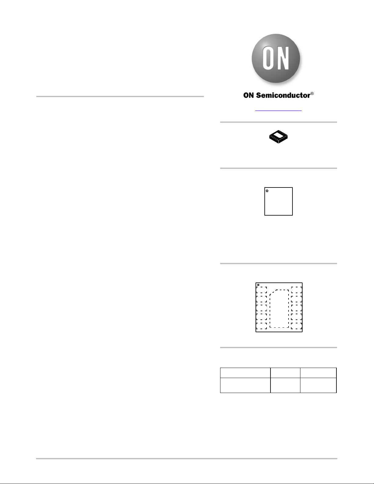
NCV7694
VS
V
BAT
C
SUPPLY
VDD_MCU
controller /
Supply for MCU and Image Sensor
VDD_MCU
Micro−
Data
interface
VDD_AR
VDD_AR
Image Sensor
AR 0135
DSP
Diag detection
GND
GND
VDD_MCU
R2
20k
FLASH
Define max
exposure time
VS
FLASH
DIAG
R
ETL
R3
R4
R
FRL
Define max
frequency
NCV7694
GND
R
EMC1
VSTR
1 kW
R
EMC2
DET
1 kW
R
EMC3
GATE
200 W
R
EMC4
FB
750 W
Note1: 4x optional
EMC shield resistors
Note2: Optional Zener diode
Q1
ZD
NVTFS5C478NL
R1
Figure 1. Application Diagram − Powered Directly from Battery
V
BAT
C
SUPPLY
VDD_MCU
Micro−
controller /
DSP
GND
Supply for MCU and Image Sensor
Data
interface
VDD_AR
VDD_AR
Image Sensor
VDD_MCU
AR 0135
Diag detection
GND
exposure time
VDD_MCU
20k
FLASH
Define max
R2
FLASH
R3
R4
DIAG
R
ETL
R
FRL
Define max
frequency
VS
NCV7694
GND
EN
C1
DC /DC
NCV898031
VString
R
VSTR
DET
GATE
FB
EMC1
1 kW
R
EMC2
1 kW
R
EMC3
200 W
R
EMC4
750 W
Note1: 4x optional
EMC shield resistors
Note2: Optional Zener diode
for Mosfet Gate protection
NVTFS5C478NL
ZD
R1
Figure 2. Application Diagram − using DC/DC
RECOMMENDED EXTERNAL COMPONENTS FOR THE APPLICATION DIAGRAM
Component Function Min Typ Max Unit
C1 Decoupling capacitor 100 nF
R1 FB current sense resistor 100
R2 DIAG pull−up resistor 20
R3 Resistor for Exposure Time Limitation 0.8 15
R4 Resistor for Frame Rate Limitation 0.8 15
REMC1 Optional EMC shield resistor for VSTR pin 1000
REMC2 Optional EMC shield resistor for DET pin 1000
REMC3 Optional EMC shield resistor for GATE pin 200
REMC4 Optional EMC shield resistor for FB pin 750
(Note 1) Optional EMC serial resistor shall be used in case
if the LEDs are detached far away from the NCV7694
device. The resistors improves the EMC susceptibility of the
application.
(Note 2) Optional Zener diode may be used if the VS
supply is higher than V
voltage of the external transistor.
GS
In case of Open Load on the LEDs, the GATE voltage will
go high, the Zener diode will limit the maximum voltage
Figure 1 shows an example of the typical output drive
configuration. The current through the external LEDs is
equal to
I
= VFB / R
LEDs
1
Where:
• V
is internal feedback reference = 300 mV
FB
• R
is feedback resistor which set the current
1
during eventual Open Load condition.
mW
kW
kW
kW
W
W
W
W
www.onsemi.com
2
Page 3
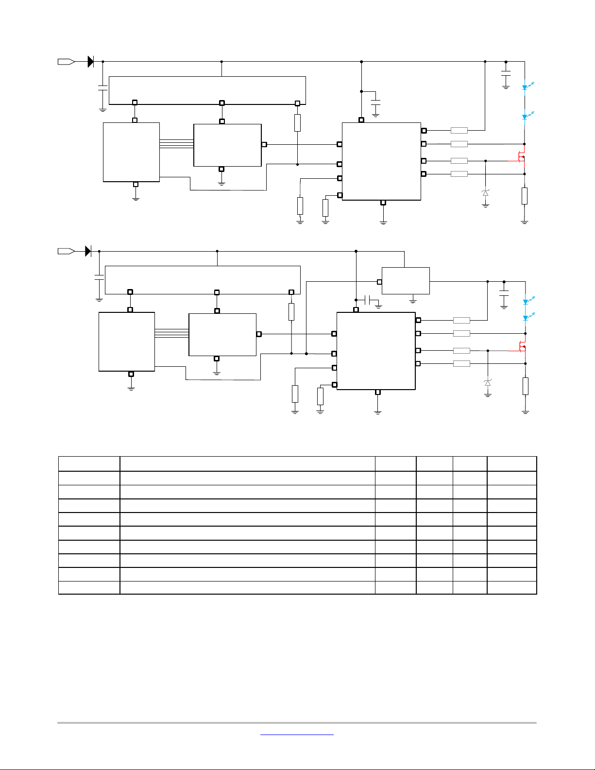
Block Diagram
Exposure
Time Limit
FLASH
DIAG
R
ETL
VS
Supply
monitoring
R
FLASH
R
=
t
ETL
K
ETL
ETL
NCV7694
Controlling,
Monitoring,
Filtering &
decoding
SC
= V
th
str
Short Circuit
LED − Vstr
Short Circuit
LED − GND
V
SVth
1.22 V
− 1.22 V
V
SGth
R
350 mV
GATE
V
STRING
DETPull−up
R
DET
GATE
R
FRL
Frame Rate
Limit
t
f
RTL
FRL
R
=
K
= 1/ t
FRL
FRL
FRL
Open Load
GND
Figure 3. Simplified Block Diagram
FB
reference
V
FBref
300mV
V
FB
150 mV
OLth
www.onsemi.com
3
Page 4
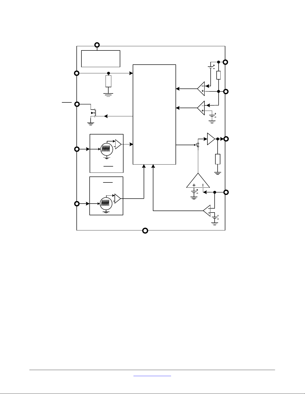
Timing Characteristics
e.g.: 45 Hz = 22 .2 ms period
NCV7694
FLASH
ET threhsold
Exposure Time
Counter
FR threshold
Frame Rate
Counter
Typical pulse
t
ETL
Too long pulse
Short pulseTypical pulse
Double frequency pulse
t
FRL
LED output
Typical pulse Short pulse
Figure 4. Simplified Internal Timing Characteristic of the Internal ETL, FRL Counter
Safety Feature Behavior
External Resistor Approach
The resistor (RETL, RFRL) creates bias voltage on the
pins. Internal oscillator speed is derived from value of the
resistors. While FLASH signal is high, internal ETL counter
is counting and when the threshold is exceeded, the output
is disabled. When FLASH pin is low, the Frame Rate timer
is starting to count. The next rising edge of the FLASH
signal is propagated to the output only if FRL timer expires.
Rest of the pulse
is cut−OFF because “ET”
counter exceed the
threshold
The period of the internals counters can be adjusted by
external resistors.
Total tolerance of the maximum T
Rate limits will be affected by internal accuracy and
accuracy of the external resistor by following equation:
Using 1% external resistor approximately 13% tolerance
can be achieved.
a
TOTAL
Driver is activated with
next rising edge of
FLASH pulse
2
Ǹ
+ a
device
) a
2
+ 13.02) 1
resistor
Second pulse is cut off
because “FR” counter is
not reach the threshold
or maximum Frame
ON
Ǹ
2
+ 13.04 %
www.onsemi.com
4
Page 5
NCV7694
PIN FUNCTION DESCRIPTION
10−pin DFN10
Package
Pin # Label Description
1 VS Supply voltage of the device
2 DIAG Diagnostic output
3 FLASH Logic input for flash exposure time
4 R
5 R
ETL
FRL
6 GND Ground
7 FB Feedback reference input 300 mV.
8 GATE Gate drive for external mosfet
9 DET LED short detection input
10 V
STRING
MAXIMUM RATINGS
Symbol Parameter Min. Max. Unit
Vmax_VS Continuous supply voltage
Vmax_FLASH Low Voltage Input pin −0.3 +3.6 V
Vmax_GATE Output voltage (during Open Load condition) −0.3 +VS V
Vmax_R
ETL
, R
FRL
Vmax_FB Low Voltage Input pin −0.3 +3.6 V
Vmax_DIAG Open Drain pin −0.3 +40 V
Vmax_DET,
V
STRING
Tjmax Junction Temperature, T
Stresses exceeding those listed in the Maximum Ratings table may damage the device. If any of these limits are exceeded, device functionality
should not be assumed, damage may occur and reliability may be affected.
1. Maximum ratings are those values beyond which device damage can occur. Maximum ratings applied to the device are individual stress limit
values (not normal operating conditions) and are not valid simultaneously. If these limits are exceeded, device functional operation is not
implied, damage may occur and reliability may be affected.
Transient Voltage (t < 500 ms, “load dump”)
DC voltage on Resistors −0.3 +3.6 V
High Voltage Input pin −0.3 +40 V
External resistor defines maximum Exposure Time Limit
External resistor defines maximum Frame Rate Limit
Short circuit reference voltage
−0.3
−
J
−40 +125
+40
+40
V
V
°C
ATTRIBUTES
Parameer Value Unit
ESD Capability (Note 2)
HBM (Human Body Model)
CDM (Charge Device Model)
MM (Machine Model)
≥ ±4.0
≥ ±1.0
≥ ±200
kV
kV
V
Moisture Sensitivity (DFN10−EP) (Note 3) 1 MSL
Storage Temperature Range −40 to 150 °C
Package Thermal Resistance (DFN10−EP) (Note 4)
− Junction to Ambient, R
− Junction to Board, R
− Junction to Case (Top), R
q
q
JB
JA
q
JC
62.5
5.5
2.7
°C/W
°C/W
°C/W
Ambient Temperature −40 to 105 °C
2. This device series incorporates ESD protection and is tested by the following methods:
ESD HBM tested per AEC−Q100−002 (EIA/JESD22−A114)
ESD CDM tested per EIA/JES D22/C101, Field Induced Charge Model
ESD MM according to AEC−Q100
3. For additional information, see or download ON Semiconductor’s Soldering and Mounting Techniques Reference Manual, SOLDERRM/D,
and Application Note AND8003/D.
4. Values represent thermal resistances under natural convection are obtained in a simulation on a JEDEC−standard, 2S2P; High Effective
Thermal Conductivity Test Board as specified in JESD51−7, in an environment described in JESD51−2a.
www.onsemi.com
5
Page 6
NCV7694
ELECTRICAL CHARACTERISTICS
(
7 V < VS < 28 V, R
R1 = 100 mW, −40°C ≤ T
GENERAL
Supply Voltage
Supply Under−Voltage Lockout VSUV VS rising 4.0 4.5 5.0 V
Supply Under−Voltage hysteresis VSUVhys 150 300 550 mV
Supply Current in normal condition I_VS
Supply Current in Fault condition I_VSerr VS = 14 V,
Thermal Shutdown (TSD) 130 150 170
Thermal Hysteresis − 15 −
FB DRIVER
FB Regulation reference
Gate ON voltage V
Propagation Delay
FLASH rising – FB ON
Propagation Delay
FLASH falling – FB OFF
FLASH propagation Delay Delta t
Output pull−down resistance R
FLASH INPUT PIN
Input High Threshold
Input Low Threshold V
Input pull−down resistance R
PROGRAMMING
R
Bias voltage V
ETL
ETL resistor operation range R
Maximum TON time (typ) T
ETL multiplication K
K
tolerance tol
ETL
Overcurrent protection R
Open Load protection R
= 4.99 kW, R
ETL
≤ 125°C, unless otherwise specified)
J
Characteristic
ETL
ETL
=1.96 kW, 4 V < V
FRL
< 28 V, Transistor = NVTFS5C478NL, LED = SFH 4725AS,
STRING
Symbol Conditions Min. Typ. Max. Unit
VS_OP Parametric operation 7 − 28 V
VS = 14 V,
− 4.0 6.0 mA
FLASH = High,
I
, I
FRL
VS = 14V,
subtracted
ETL
− 3.8 6.0 mA
FLASH = Low,
I
, I
FRL
subtracted
ETL
− 4.0 6.0 mA
FLASH = High,
Open Load condition,
I
, I
subtracted
ETL
4.5 − − V
− 1.4 4
V
FBref
GATE
t
ON
t
OFF
pd_delta
FRL
Under Voltage Lockout < VS 270 300 330 mV
FB = 220 mV,
DET = 1.0 V
50% criterion − 8 15
50% criterion − 6.6 15
|(Falling time) –
(Rising Time)|
50% criterion
GATE
V
inH
inL
FLASH
ETL
ETL
ONmax
ETL
ETL
I
ETL_lim
I
ETL_open
5 30 100
1.3 1.2 − V
− 1.15 1.1 V
30 120 190
I
ETL
V
+
R
ETL
ETL
1.0
+
4990
+ 200.4 mA
external resistor value operation
− 1.0 − V
0.8 − 15
range
for R
for R
Derived from R
valid for
K
t
ETL
ETL
= 800 W => t
ETL
= 15 kW => t
ETL
R
ETL
R
ETL
+
t
ETL
R
ETL
+
K
ETL
and K
ETL
= 15 kW
4.99
+
2.5
= 320 ms;
ETL
= 6 ms
ETL
ETL(typ)
+ 1.996 ms
;
− − 6.0 ms
− 2.5 −
Tolerance of Exposure Time Limit ±13.0 %
Short to ground
1.3 − − mA
Resistor detection for
< 750 W
R
ETL
Open Load detection
− − 57.5
Resistor detection for
> 17.5 kW
R
ETL
°C
°C
μs
μs
μs
kW
kW
kW
kW/s
mA
www.onsemi.com
6
Page 7

ELECTRICAL CHARACTERISTICS
(
7 V < VS < 28 V, R
R1 = 100 mW, −40°C ≤ T
PROGRAMMING
FRL resistor
operation range
= 4.99 kW, R
ETL
≤ 125°C, unless otherwise specified)
J
FRL
Characteristic UnitMax.Typ.Min.ConditionsSymbol
=1.96 kW, 4 V < V
R
FRL
NCV7694
< 28 V, Transistor = NVTFS5C478NL, LED = SFH 4725AS,
STRING
external resistor value operation
range
for R
FRL
(10 ms)
for R
FRL
(100 ms)
= 1 kW => f
= 10 kW => f
FRL
FRL
=100 Hz
=10Hz
0.8 − 15
kW
Maximum FLASH Frequency (typ) f
FRL multiplication K
K
tolerance tol
FRL
Overcurrent protection R
Open Load protection R
FRL
FRL
I
I
FRL_open
OPEN LOAD / SHORT TO GND
Open Load Detection Threshold (FB pin)
Open Load
t
Blanking Time
Short to GND Detection Threshold
(DET pin)
Short to GND
t
Blanking Time
SHORT CIRCUIT
Short to V
Detection Threshold V
STRING
Short Circuit Blanking Time t
Input pull−up resistor on DET pin R
DETPull−up
DIAG OUTPUT
V
diagnostic activation threshold V
STRING
max
FRL
FRL
FRL_lim
V
OLth
OLBlank
V
SGth
SGBlank
SCth
SCBlank
STRth
Derived from R
valid for R
R
K
+
FRL
t
R
t
f
FRL
FRL
FRL
+
K
FRL
1
+
t
FRL
FRL
FRL
FRL
+
+
and K
FRL
= 800 W
1.96
0.1
1
0.0196
FRL(typ)
+ 19.6 ms
+ (51 Hz)
;
− − 125 Hz
−
0.1
−
Tolerance of Frame Rate Limit ±13.0 %
Short to ground
1.3 − − mA
Resistor detection for
< 750 W
R
FRL
Open Load detection
− − 57.5
Resistor detection for
> 17.5 kW
R
FRL
FLASH = High 130 150 170 mV
10 22 35
FLASH = Low 300 350 400 mV
5 10 15
FLASH = High V
ING
STR
1.5
V
−
ING
1.22
STR
V
STR
−
ING
0.9
−
5 10 15
Pull−up to V
V
voltage 2.0 2.2 2.4 V
STRING
STRING
30 120 190
mA
ms
ms
V
ms
kW
Output low level V
OUTL
www.onsemi.com
Fault is present,
I
DIAG
7
= 0.33 mA
− 0.2 0.4 V
Page 8

NCV7694
PINS DESCRIPTION
FLASH
Flash Input pin is compatible with 1.8 V / 2.8 V logic of
the ON Semiconductor image sensors. Internal pull down
resistor is implemented to prevent unwanted switch on.
Based on the R
ETL
and R
resistors, the maximum T
FRL
ON
FLASH time which can be propagated to the output is 6 ms
and minimum T
time, which will can be set, is typically
OFF
8 ms. The NCV7694 can be used as companion device for
60 Hz camera sensors in full FLASH T
with limited T
DIAG
ON
range.
range or 120 Hz
ON
Open Drain DIAG pin can be connected with pull up
resistor to MCU which will be informed about a fault in case
of Open Load, Short to V
or Short to Ground of the
STRING
LEDs. Diagnostic pin can be connected to the Enable pin of
the DC/DC converter. The output V
STRING
voltage will be
disconnected and user and devices are protected against
damages. The NCV7694 driver can also inform the system
while FLASH pulse is too long or is send too frequent. The
Open Load and Short circuit detections of the R
ETL
, R
FRL
timing resistors are reported on the DIAG pin as well as the
Thermal Shutdown Flag and Under Voltage status on the VS
supply.
DET
Detection pin is sensing the voltage at the cathode of the
LEDs. The voltage on DET pin during the FLASH−ON
period should be in range from V
(V
Short to ground and above V
will detect Short LEDs to V
– 1.22 V). Below 0.35 V the device will detect
STRING
STRING
STRING
(0.35 V) to V
SGth
SVth
minus 1.22 V the device
.
In case of DET pin is disconnected, device will go into
fault because internal pull−up to V
is implemented.
STRING
Short to ground can be detected only when output is not
activated.
FB
A feedback loop regulates the current through the external
LEDs. The voltage across the external sense resistor is
regulated to the 300 mV typ. Using FB pin can be detected
Open Load condition, if the when FB voltage will be below
threshold for longer than blanking time. It is not allowed to
put external voltage higher than 0.19 V on the FB pin when
the device is not active. The voltage on the FB pin has to be
below 0.19 V during VS supply ramp up while FLASH
PWM signal is already present.
GATE
The NCV7694 can drive MOSFET transistors with
minimum GATE voltage of 4.5 V. The preferred mosfet
transistor is NVTFS5C478NL.
R
and R
ETL
FRL
To reduce thermal retina hazard and thermal injury risk of
the cornea, the safety turn−off function is implemented.
External R
ETL
and R
resistor defines maximum
FRL
exposure time and maximum frame rate. The maximum
times are calculated using resistor values of the R
resistors divided by K
R
FRL
FRL
or K
coefficients. If the
ETL
ETL
and
FLASH pulse is permanently HIGH, the output pulse is
being activated only after FRL timer expire and during the
allowed ETL time period.
Short and Open on the R
ETL
and R
FRL
To be able detect the defect on the external resistors the
Open Load and Short to Ground detections are implemented
in the NCV7694. If the resistor value will be below 750 W,
short to ground will be detected. If the resistor value
becomes higher than 17.5 kW, Open Load is detected.
As soon as a fault condition is detected, then after a short
filter time the driver is switched off and fault on the DIAG
pin is reported
V
STRING
High voltage input pin sense the voltage on the top of the
LEDs and enable the Open Load and Short diagnostic as
soon as the voltage exceed the threshold VSTRth >2.2 V. If
DC/DC converter is not used, the VSTRING voltage has to
be connected to the VS pin. If the LED diagnostic is not
required, then the VSTRING pin has to be grounded.
www.onsemi.com
8
Page 9

NCV7694
DETAILED OPERATING DESCRIPTION
Under Voltage Lockout
Under voltage Lockout feature is used to protect against
an abnormal status during startup. When the initial soft start
voltage is greater than 4.5 V (typ) the device starts to be
active. Below this threshold the GATE output pin is pulled
low to ground to prevent opening external N−MOS
transistor and DIAG pin is pulled low to report.
Thermal Shutdown
The thermal shutdown circuit checks the internal junction
temperature of the device. When the internal temperature
rises above the Thermal shutdown threshold, then after a
short filter time the driver is switched off and fault on the
DIAG pin is reported.
Exceeding the Flash Pulse
If the duration of the FLASH pulse exceeds the
pre−defined timing or the FLASH pulse repetition is too
frequent, the GATE of the transistor is switched off. The
limitation of the FLASH pulses is also reported on the DIAG
pin. The first FLASH pulse after power−on−reset should be
delayed longer than FRL period, otherwise the FLASH
pulse will be limited and DIAG pin will report a fault until
FRL counter expires.
www.onsemi.com
9
Page 10

Open Load Detection
V
BAT
NCV7694
VDD_MCU
20 kW
FLASH = High
FLASH
DIAG
Define
exposure
R2
R3
max
time
FLASH
R4
Define
max
frequency
DIAG
R
R
FRL
ETL
VS
GND
Figure 5. Open Load Detection Circuit
When Open Load fault is introduced during
FLASH = High and V
STRING
> V
, the 22 ms blanking
STRth
time eliminate the false faults. When blanking time expires,
the NCV7694 immediately report a fault on the DIAG pin.
The output GATE pin remains active. The DIAG pin is
recovered with the falling edge on the FLASH pin or after
ETL counter is expired.
If EN pin of the DC/DC converter is connected to the
DIAG output, the Open Load causes switching OFF the
V
voltage. The DIAG pin is recovered as soon as
STRING
FLASH pin goes low or ELT counter expired. It will take
> V
VFB <
V
STRING
STRth
150 mV
Open Load
R1
EN
C1
NCV7694
DC /DC
NCV898031
VSTR
V
STRING
DET
GATE
FB
approximately 2 ms to re−activate the DC/DC V
voltage of the converter. With typical FRL setting, the driver
will be ready to perform the diagnostic on the next FLASH
pulse.
If the ENable of the DC/DC converter is not driven by
NCV7694, the Open Load is reported to the DIAG pin.
Diagnostic is not active when V
STRING
< V
STRth
FLASH pulse will not be detected when driver is going to be
recovered from a Short to GND fault because the DC/DC
converter in not fully active.
STRING
. The first
www.onsemi.com
10
Page 11

STRING
V
DET
V
V
STRth
2.2 V
NCV7694
OPEN LOAD BEHAVIOR
Conditions: VS powered, DC /DC used, EN connected to the DIAG pin
Open Load present
input
FLASH
GATE
V
DIAG
V
FLASH is
propagated
to the output
t
DC_EN
Fault is present
and detected
LED is OFF
t
OLBlank
t
DC_EN
t
= 1.5 ms activation delay of the DC/DC
DC_EN
V
STRING
is not
sufficient, Open
Load isn’t detected
Figure 6. Timing of the Open Load Behavior
www.onsemi.com
11
Page 12

NCV7694
Short to Ground
In case of short to ground, huge amount of current is
passing through the LEDs. To protect the LEDs and Human
eyes, the safety mechanism can be implemented. The DIAG
V
BAT
VDD_MCU
20 kW
FLASH = Low
FLASH
DIAG
exposure
R2
R3
Define
max
time
R4
Define
max
frequency
FLASH
DIAG
R
ETL
R
FRL
VS
EN
C1
NCV7694
GND
output diagnostic pin can be connected directly to the Enable
of the DC/DC converter. In case of fault, the DC/DC
converter is automatically disabled after blanking times.
V
DC / DC
NCV898031
VSTR
DET
GATE
FB
STRING
High LED current
V
<
350 mV
DET
R1
Short DET
pin to Ground
Figure 7. Short to Ground Detection Circuit
When Short to Ground is introduced during
V
STRING
> V
and FLASH is low, the 10 ms blanking
STRth
time eliminate the false faults. When blanking time expires,
the NCV7694 immediately report a fault on the DIAG pin
which leads to the switching OFF the V
STRING
voltage to
protect the LEDs. The output GATE pin remains active. The
device is recovered with next rising edge on the FLASH
input pin. (The next FLASH pulse will not be propagated to
the output, because the DC/DC converter is not activated).
The microprocessor can distinguish between Short to
GND and Open Load during FLASH = Low. If the DIAG pin
remains low during FLASH = Low, the Short to Ground was
detected and it is not recommended to not turn ON the
V
STRING
voltage.
www.onsemi.com
12
Page 13

STRING
V
DET
V
V
)
F
–V
STRING
(V
NCV7694
BEHAVIOR OF THE SHORT TO GND
Conditions: VS powered, DC /DC used, EN connected to the DIAG pin
Short to GND
STRth
2.2V
input
FLASH
GATE
V
DIAG
V
FLASH is
propagated
to the output
t
Fault is present
and detected
LEDs are OFF
Figure 8. Timing of the Short to GND Behavior
t
SGBlank
= 1.5 ms activation delay of the DC/DC
DC_EN
V
STRING
is not
t
SGBlank
sufficient, Open
Load isn’t detected
t
DC_EN
t
DC_EN
*) DIAG latched until next FLASH rising edge
www.onsemi.com
13
Page 14

Short to VS
NCV7694
VBAT
VDD_MCU
FLASH = High
FLASH
DIAG
R2
20 kW
R3
Define
max
exposure
time
R4
Define
max
frequency
FLASH
DIAG
R
ETL
R
FRL
VS
EN
NCV7694
GND
Figure 9. Short to VSTRING Detection Circuit
When Short Cathode of the LEDs to V
STRING
voltage is
introduced during the FLASH = High and
V
STRING
> V
, the 10 ms blanking time eliminate the
STRth
false faults. When the blanking time expires, the NCV7694
immediately switch OFF the GATE output to protect the
external transistor against high power dissipation. The
DIAG pin will report a fault which will lead to switching
OFF the DC/DC V
voltage if the DIAG pin is
STRING
C1
DC / DC
NCV898031
V
STRING
>V
STRth
V
STRING
VSTR
V
DET
> (V
STRING
– 1.22)V
DET
GATE
GATE − OFF
FB
High
transistor
current
R1
connected to the Enable of the DC/DC converter. The fault
is latched during the FLASH signal is high or until ETL
counter expires. The device will be recovered only with next
falling edge on the FLASH or when the ETL counter is
expired.
The diagnostic is not active when V
STRING
< V
STRth
or
also during FLASH = Low.
www.onsemi.com
14
Page 15

NCV7694
Behavior of the Short to V
Conditions: VS powered, DC /DC used, EN connected to the DIAG pin
V
STRth
STRING
V
2.2V
DET
V
input
FLASH
STRING
:
Short to V
STRING
t
DC _E N
GATE
V
DIAG
V
FLASH is
propagated
to the output
t
SCBlank
t
SCBlank
Fault is present
and detected
LED is OFF
Fault is present
GATE is ON during
blanking time only
Figure 10. Timing of the Short to VSTRING Behavior
www.onsemi.com
15
Page 16

Overview of the Faults
NCV7694
Normal
Operation
Open
Load
OFF
DET_PULL UP
OFF
DET_PULL UP
OFF ONFLASH =
V
STRING
VSTR
DET
GATE
FB
V
STRING
VSTR
DET
GATE
FB
V
~V
STRING
disabled
V
~ V
STRING
disabled
STRING
R1
STRING
~ 0V
R1
0 V
~ V
STRING
V
STRING >VSTRth
LEDs
are OFF
LEDs
are OFF
ON
ON
V
STRING
VSTR
DET
GATE
FB
V
STRING
VSTR
DET
GATE
FB
V
V
STRING –VF_LEDs
enabled
300mV
V
~ 0V
enabled
~ 0.0mV
STRING
R1
STRING
R1
~ V
STRING
V
STRING >VSTRth
LEDs
are ON
LEDs
are OFF
Short to
Ground
Short to
V
STRING
OFF
DET_PULL UP
OFF
DET_PULL UP
Unrecognizable
V
STRING
VSTR
DET
GATE
disabled
FB
DET < 0.35 V
V
STRING
VSTR
DET
GATE
disabled
FB
Unrecognizable
V
STRING
0V
0.0mV
V
STRING
V
STRING
DET < 0.35 V
or FB < 150
ON
LEDs are
stressed
LED
DC/DC can
disable
High I
V
STRING
R1
Fault is latched
until next rising
DET < 0.35 V
or FB < 150
ON
V
STRING
VSTR
DET
GATE
FB
V
STRING
mV
enabled
~ 0.0mV
mV
V
0V
V
STRING
R1
STRING
LEDs are
stressed
LED
DC/DC can
High I
disable
V
STRING
Same as
Open Load
condition
MOSFET is
stressed
DC/DC can
D(N−MOS)
High P
disable
V
STRING
0V
R1
LEDs
are OFF
DET > (V
VSTR
DET
GATE
FB
STRING
ON
enabled
300 mV
1.22 V)
–
V
STRING
R1
Figure 11. Overview of the Faults
www.onsemi.com
16
Page 17
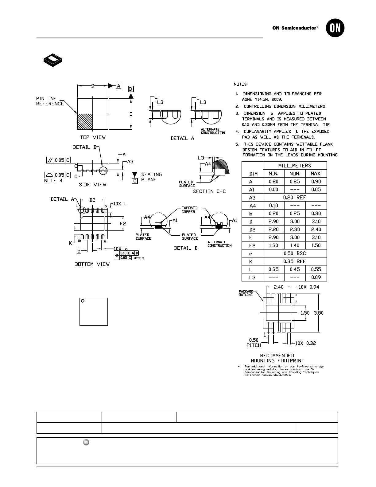
MECHANICAL CASE OUTLINE
PACKAGE DIMENSIONS
1
SCALE 2:1
DFNW10, 3x3, 0.5P
CASE 507AG
ISSUE B
DATE 14 APR 2020
GENERIC
MARKING DIAGRAM*
1
XXXXX
XXXXX
ALYWG
G
XXXXX = Specific Device Code
A = Assembly Location
L = Wafer Lot
Y = Year
W = Work Week
G = Pb−Free Package
(Note: Microdot may be in either location)
*This information is generic. Please refer to
device data sheet for actual part marking.
Pb−Free indicator, “G” or microdot “ G”,
may or may not be present. Some products
may not follow the Generic Marking.
DOCUMENT NUMBER:
DESCRIPTION:
ON Semiconductor and are trademarks of Semiconductor Components Industries, LLC dba ON Semiconductor or its subsidiaries in the United States and/or other countries.
ON Semiconductor reserves the right to make changes without further notice to any products herein. ON Semiconductor makes no warranty, representation or guarantee regarding
the suitability of its products for any particular purpose, nor does ON Semiconductor assume any liability arising out of the application or use of any product or circuit, and specifically
disclaims any and all liability, including without limitation special, consequential or incidental damages. ON Semiconductor does not convey any license under its patent rights nor the
rights of others.
98AON73716G
DFNW10, 3x3, 0.5P
Electronic versions are uncontrolled except when accessed directly from the Document Repository.
Printed versions are uncontrolled except when stamped “CONTROLLED COPY” in red.
PAGE 1 OF 1
© Semiconductor Components Industries, LLC, 2018
www.onsemi.com
Page 18

ON Semiconductor and are trademarks of Semiconductor Components Industries, LLC dba ON Semiconductor or its subsidiaries in the United States and/or other countries.
ON Semiconductor owns the rights to a number of patents, trademarks, copyrights, trade secrets, and other intellectual property. A listing of ON Semiconductor ’s product/patent
coverage may be accessed at www.onsemi.com/site/pdf/Patent−Marking.pdf
ON Semiconductor makes no warranty, representation or guarantee regarding the suitability of its products for any particular purpose, nor does ON Semiconductor assume any liability
arising out of the application or use of any product or circuit, and specifically disclaims any and all liability, including without limitation special, consequential or incidental damages.
Buyer is responsible for its products and applications using ON Semiconductor products, including compliance with all laws, regulations and safety requirements or standards,
regardless of any support or applications information provided by ON Semiconductor. “Typical” parameters which may be provided in ON Semiconductor data sheets and/or
specifications can and do vary in different applications and actual performance may vary over time. All operating parameters, including “Typicals” must be validated for each customer
application by customer’s technical experts. ON Semiconductor does not convey any license under its patent rights nor the rights of others. ON Semiconductor products are not
designed, intended, or authorized for use as a critical component in life support systems or any FDA Class 3 medical devices or medical devices with a same or similar classification
in a foreign jurisdiction or any devices intended for implantation in the human body. Should Buyer purchase or use ON Semiconductor products for any such unintended or unauthorized
application, Buyer shall indemnify and hold ON Semiconductor and its officers, employees, subsidiaries, affiliates, and distributors harmless against all claims, costs, damages, and
expenses, and reasonable attorney fees arising out of, directly or indirectly, any claim of personal injury or death associated with such unintended or unauthorized use, even if such
claim alleges that ON Semiconductor was negligent regarding the design or manufacture of the part. ON Semiconductor is an Equal Opportunity/Affirmative Action Employer. This
literature is subject to all applicable copyright laws and is not for resale in any manner.
. ON Semiconductor reserves the right to make changes without further notice to any products herein.
PUBLICATION ORDERING INFORMATION
LITERATURE FULFILLMENT:
Email Requests to: orderlit@onsemi.com
ON Semiconductor Website: www.onsemi.com
TECHNICAL SUPPORT
North American Technical Support:
Voice Mail: 1 800−282−9855 Toll Free USA/Canada
Phone: 011 421 33 790 2910
Europe, Middle East and Africa Technical Support:
Phone: 00421 33 790 2910
For additional information, please contact your local Sales Representative
◊
www.onsemi.com
1
 Loading...