

Page 1
Controller for Automotive
LED Lamps
NCV7693
The NCV7693 is a device which drives multiple external switching
components for 3 independent functions. The average current in each
LED string can be regulated with a proper choice of duty−cycle and
battery voltage. The target application for this device is automotive
rear combination lamps. Each individual driver has its own diagnostic
to detect open load, short circuit to ground or to battery.
LED average brightness levels are easily programmed using
appropriate duty cycle control and external resistors in series with the
switching transistors.
Multiple strings of LEDs can be operated with a single NCV7693
device. The device is available in a TSSOP−14 package.
Features
• 3x Pulse Width Modulation (PWM) Control
• Independent Diagnostic Feedback per Function
• External Switching Device for Wide Current Range Flexibility
• External Resistors Define Maximum Current
• Open LED String Diagnostic
• Short−Circuit LED String Diagnostic
• Thermal Shut−down Diagnostic and Protection
• Protection against Short−Circuit on the PWM Input Pins
• Multiple LED String Control
• TSSOP−14 Package
• AEC−Q100 Qualified and PPAP Capable
• These Devices are Pb−Free, Halogen Free/BFR Free and are RoHS
Compliant
Applications
• Rear Combination Lamps (RCL)
• Daytime Running Lights (DRL)
• Fog Lights
• Center High Mounted Stop Lamps (CHMSL) Arrays
• Turn Signal and Other Externally Modulated Applications
• General Automotive LED Driver
www.onsemi.com
14
1
TSSOP−14 WB
CASE 948G
MARKING DIAGRAM
14
NCV
7693
ALYWG
G
1
A = Assembly Location
L = Wafer Lot
Y = Year
W = Work Week
G = Pb−Free Package
(Note: Microdot may be in either location)
ORDERING INFORMATION
Device Package Shipping
NCV7693DB0R2G TSSOP−14
(Pb−Free)
†For information on tape and reel specifications,
including part orientation and tape sizes, please
refer to our Tape and Reel Packaging Specifications
Brochure, BRD8011/D.
2500 /
Tape & Reel
†
© Semiconductor Components Industries, LLC, 2017
December, 2019 − Rev. 1
1 Publication Order Number:
NCV7693/D
Page 2
VSupply
NCV7693
PWM 1
PWM 2
PWM 3
VS
FB1
SW1
IO1
IO2
FB2
SW2
IO3
n.c.
FB3
SW3
TSTEN
n.c.
GND
Figure 1. Application Diagram
R1
R2
R3
www.onsemi.com
2
Page 3
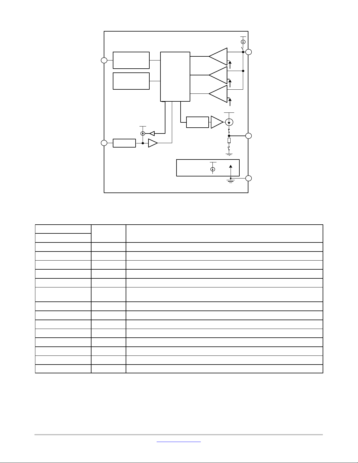
NCV7693
VS
VS
IOx
PIN FUNCTION DESCRIPTION
TSSOP−14 Package
Pin #
1 VS Automotive Battery input voltage
2 IO1 Logic input1 for output SW1 on / off control and diagnostic feedback. Pull high for output on.
3 IO2 Logic input2 for output SW2 on / off control and diagnostic feedback. Pull high for output on.
4 IO3 Logic input3 for output SW3 on / off control and diagnostic feedback. Pull high for output on.
5 NC Not connected
6 TSTEN Pin used for test purpose only, has to be connected to GND pin during the normal
7 NC Not connected
8 GND Ground
9 SW3 Switch Driver 3 for external transistor
10 FB3 Feedback pin for error detection on SW3
11 SW2 Switch Driver 2 for external transistor
12 FB2 Feedback pin for error detection on SW2
13 SW1 Switch Driver 1 for external transistor
14 FB1 Feedback pin for error detection on SW1
Label Description
Supply
Monitoring
Thermal
Monitoring
Protection
3.15V
7mA
operation.
OL
Error
Monitoring
Filtering
& decoding
SC _GND
SC _VS
Slew Rate
Control
Reference
Voltages
and Currents
Figure 2. Block Diagram
+
+
+
Refx
−
−
−
5.5V
FBx
Ref 1
Ref 2
Ref 3
SWx
GND
www.onsemi.com
3
Page 4
MAXIMUM RATINGS
(Voltages are with respect to GND, unless otherwise specified)
NCV7693
Rating
Value Unit
Supply Voltage (VS)
DC
Peak Transient
−0.3 to 50
50
V
V
High Voltage Input−Output Pins (IO1, IO2, IO3) −40 to 50 V
High Voltage Input Pins (FB1, FB2, FB3) −0.3 to 50 V
Low Voltage Pins (SW1, SW2, SW3) −0.3 to 6.5 V
Junction Temperature, T
J
−40 to 150 °C
Peak Reflow Soldering Temperature: Pb−Free, 60 to 150 seconds at 217°C (Note 1) 260 peak °C
Stresses exceeding those listed in the Maximum Ratings table may damage the device. If any of these limits are exceeded, device functionality
should not be assumed, damage may occur and reliability may be affected.
1. For additional information, please see or download the ON Semiconductor Soldering and Mounting Techniques Reference Manual,
SOLDERRM/D and Application Note AND8003/D.
ATTRIBUTES
Characteristic Value
ESD Capability
Human Body Model without any filter all Iox versus GND and VS versus GND
Charge Device Model
Moisture Sensitivity MSL2
Storage Temperature Range −55 to 150°C
Package Thermal Resistance − TSSOP−14 (Note 3)
Junction–to–Ambient, R
Junction–to–Case, R
q
JA
Y
JC
2. Minimum ±2 kV HBM for all pin combinations.
3. Values represent typical still air steady−state thermal performance on 1 oz. copper FR4 PCB with 650 mm
±6.0 kV (Note 2)
≥ ±750 V
135°C/W
45°C/W
2
copper area.
www.onsemi.com
4
Page 5

NCV7693
ELECTRICAL CHARACTERISTICS
(6.17 V < VS < 16 V, Transistor NPN = BCP56 or NMOS = NVR5198, −40°C ≤ TJ ≤ 150°C, unless otherwise specified) (Note 4)
Characteristic Conditions Min Typ Max Unit
General Parameters
Supply Current
VS = 14 V, all IOx > 2.2 V, SWx current subtracted
VS = 14 V, all IOx = 0 V
Under Voltage Lockout VS rising (Note 5) 2.24 3.35 4.43 V
Under Voltage Lockout Hysteresis (Note 5) − 500 − mV
Thermal Shutdown (TSD) (Note 5) 155 170 190 °C
Thermal Hysteresis (Note 5) − 15 − °C
Switch Driver
Output Source Current
SWx = 0.7 V (Note 6), −40°C ≤ TJ ≤ +25°C 25 50 − mA
Output Source Current SWx = 0.7 V (Note 6), +25°C ≤ TJ ≤ +125°C 15 30 − mA
Output Source Current SWx = 0.7 V (Note 6), +125°C ≤ TJ ≤ +150°C 7.0 15 − mA
Swx ON Voltage
ISWx = −100 mA, 7 V < VS < 19 V
ISWx = −100 mA
Open Load Timing
Open Load Detection Threshold
IOx High 0.7 0.85 1.0 V
Open Load Blanking Time 10 22 35
Short Circuit to VS
Short Circuit Detection Threshold
IOx High VS−1.0 VS−1.2 VS−1.4 V
Input pull−up current on FBx pins Tested at V(FBx) = VS − 1.0 V −35 −20 −2.0
Short Circuit Blanking Time Tested at 15 V 5.0 10 15
Short Circuit to Ground
Short Circuit Detection Threshold
IOx Low 0.7 0.85 1.0 V
Short Circuit Blanking Time Tested at 15 V 10 22 35
IOx
Input High Threshold
Input Low Threshold 1.1 − − V
Hysteresis − 0.52 − V
Input Pull−down Resistor Tested at V(IOx) = 15 V 75 150 300
IOx Clamp Voltage in error mode PWMx > 5 V, 2 mA < I(IOx) < 9.5 mA 2.80 3.15 3.46 V
AC Characteristics
Propagation Delay
IOx rising to Iout
Propagation Delay
IOx falling to Iout
Propagation Delay
IOx rising to Vout
Propagation Delay
IOx falling to Vout
BJT
BJT
NMOS
NMOS
50% criterion (Note 7) − 5 15
50% criterion (Note 7) − 5 15
From IOx input high threshold to 90% rising of
SWx_ON Voltage, C
= 470 pF
load
From IOx input low threshold to 10% falling of
SWx_ON Voltage, C
= 470 pF
load
Product parametric performance is indicated in the Electrical Characteristics for the listed test conditions, unless otherwise noted. Product
performance may not be indicated by the Electrical Characteristics if operated under different conditions.
4. Designed to meet these characteristics over the stated voltage and temperature recommended operating ranges, though may not be 100%
parametrically tested in production.
5. Guaranteed by design.
6. This current is designed to decrease over temperature in case the switching element is an external bipolar to compensate internal heating
and Beta.
7. Evaluated at VS = 14V.
2.2
30
4.5
4.5
5.2
185
5.5
−
10
380
6.5
−
− − 2.2 V
− − 5
− − 5
mA
mA
V
V
ms
mA
ms
ms
kW
ms
ms
ms
ms
www.onsemi.com
5
Page 6

NCV7693
TYPICAL PERFORMANCE CHARACTERISTICS
Equivalent schematics
The following figure gives the equivalent schematics of the user relevant inputs and outputs. The diagrams are simplified
representations of the circuits used.
VS
VS
μA
VS
IOx
VS
Type 1: VS supply pin
3.15V
I
=7mA
fault
Pull−down
150kW
Fault
PWMx_ON / OFF
Low Power mode
OL, SC_ GND
SC_VS
Type 2: FBx input pins
Slope Control / current derating
SWx_ON / OFF / Low power mode
V
V
REF 1
REF 2
5.5V
VS
1kW
Pull−down
= 10+10= 20
FBx
I
=7−50mA
SWx
I
FBx
SWx
Type 3: IOx output pins
Type 4: SWx output pins
Figure 3. Input and Output Equivalent Diagrams
www.onsemi.com
6
Page 7

NCV7693
Detailed Operating Description
The NCV7693 device provides low−side current drive via
an external switching transistor in series with the LEDs and
a resistor. The drop across the resistor plus either the V
the V
of the transistor is supposed to be above 1V in
DS
CE
or
normal operation. Dimming is performed using the
dedicated PWM at the IOx pins of the IC.
Output Drive
Figure 4 shows an example of the typical output drive
configuration. The average current through the external
LED is equal to:
Vsupply
I
LED
+
ǒ
VS * VF* V
R
10kΩ
10kΩ
Ǔ
DROP
DC
optional
1.5kW+/−5%
Where;
VS is the Automotive Battery input voltage,
V
is the sum of the forward voltage of the LEDs,
F
V
DROP
BJT) or V
is either V
(in case NMOSFET is chosen),
DS
(saturation voltage of the chosen
CEsat
DC is the Duty Cycle present at the input of the IOx pins
and
R the series resistance with the LEDs (typical value range
is in between 50 and 100 W).
optional
100nF
VS
FBx
from
NCV7693
4.7k
+/−5%
IOx
W
TSTEN
SWx
GND
μC
30kΩ
μC
to
10kΩ
PWM / DIAG
C1
2.2nF
2.2nF
Figure 4. Output Drive configuration
www.onsemi.com
7
Page 8

NCV7693
Open Load Detection
Faulted output strings due to open load conditions
sometimes require detection in an automotive rear lighting
system. The NCV7693 provides that feature.
When LED driver is ON (PWM is active high) and when
the voltage on the FBx pin is detected below 0.85 V for more
Vsupply
10kΩ
optional
1.5kW+/−5%
10kΩ
from
μC
30kΩ
μC
to
10kΩ
PWM / DIAG
C1
2.2nF
2.2nF
Figure 5. Open Load Detection
than 22 ms typical then an open load error is activated. The
IOx pin is pulled down to 3.15 V typical allowing the
mcontroller to detect the error when the PWM input signal
is activated High. During open load condition the driver
stays active. If the open load disappears the device is
working properly again and the diagnostic flag disappears.
optional
100nF
4.7k
+/−5%
VS
NCV7693
IOx
W
TSTEN
FBx
SWx
GND
*recommended if MOSFET is used
10kΩ
*
or
www.onsemi.com
8
Page 9

NCV7693
Short Circuit to Ground Detection
The FeedBack (FBx) pins of the device are used as inputs
to detect a fault when the resistor on top of either the
collector or the drain of the external transistor is shorted to
Ground. When LED driver is OFF (PWM is low) and when
the voltage on the FBx pin is detected below 0.85 V for more
than 22 ms typical then a SC to Ground is latched. The IOx
pin is then pulled down to 3.15 V typical allowing the
Vsupply
10kΩ
optional
1.5kW+/−5%
10kΩ
from
μC
30kΩ
μC
to
10kΩ
PWM / DIAG
C1
2.2nF
2.2nF
Figure 6. Short Circuit to Ground Detection
mcontroller to detect the error when the PWM input signal
is activated High. During SC to Ground condition the driver
stays active. If the short circuit disappears the device is
working properly on next falling edge of the PWM input pin.
If at least one IOx pin remains High, then short to Ground
detection is guaranteed. Note that in case all IOx pins are
Low, the device is in low power mode and a short to Ground
cannot be detected.
optional
100nF
4.7k
+/−5%
VS
NCV7693
IOx
W
TSTEN
FBx
SWx
GND
*recommended if MOSFET is used
10kΩ
or
*
www.onsemi.com
9
Page 10

NCV7693
Short Circuit to VS Detection
The FeedBack (FBx) pins of the device are used as inputs
to detect a fault when the resistor on top of either the
collector or the drain of the external transistor is shorted to
the battery voltage. This error is detected when the driver is
ON (PWM active High). The threshold voltage detection is
referenced 1.2 V typical down from the VS pin. A voltage
of less than 1.2 V between VS and FBx for more than 10 ms
then a SC to VS is detected. The IOx pin is then pulled down
Vsupply
10kΩ
optional
1.5kW+/−5%
10kΩ
from
μC
30kΩ
μC
to
10kΩ
PWM / DIAG
C1
2.2nF
2.2nF
Figure 7. Short Circuit to VS Detection
to 3.15 V typical allowing the mcontroller to detect the error
when the PWM input signal is activated High. Because of
the large power dissipation possible during this error, the
driver is switched OFF. If the SC disappears the device is
working properly on next rising edge of the PWM input pin.
In case multiple strings are connected to the same driver (see
Figure 9), this error is only detected at the condition each
string is shorted to VS (a single string detection is not
detected because of the blocking diodes).
optional
100nF
4.7k
+/−5%
VS
NCV7693
IOx
W
TSTEN
FBx
SWx
GND
*recommended if MOSFET is used
10kΩ
or
*
Thermal shut down
The thermal shut down circuit checks the internal junction
temperature of the device. When the internal temperature
rises above the Thermal shutdown threshold, then after a
short filter time the output channels are switched off. The
filter is implemented to avoid parasitic TSD, switching off
the driver in case of TSD, will also make the IOx pin is then
pulled down to 3.15 V typical allowing the mcontroller to
detect the error when the PWM input signal is activated
High. It is the responsibility of the mcontroller to
switch−OFF all IOx when the error is detected to avoid large
power dissipation in the device due to the large current
flowing in the IOx pins.
www.onsemi.com
10
Page 11

NCV7693
Vsupply
Vsupply
from
6.5V
10kΩ
DC/DC
Automotive Grade
(example: NCV8853
buck controller)
100nF
optional
W
1.5k
+/−5%
VS
FBx
10kΩ
NCV7693
4.7k
+/−5%
IOx
SWx
or
W
TSTEN
GND
10kΩ
*
μC
PWM / DIAG
30kΩ
μC
to
10kΩ
C1
2.2nF
2.2nF
*recommended if MOSFET is used
Figure 8. Application diagram with a DC/DC
optional
10kΩ
from
100nF
optional
1.5kW+/−5%
VS
FBx
10kΩ
NCV7693
4.7k
+/−5%
IOx
SWx
W
TSTEN
GND
μC
PWM / DIAG
30kΩ
μC
to
10kΩ
C1
2.2nF
2.2nF
or or
*
10kΩ
*recommended if MOSFET is used
Figure 9. Application diagram with multiple strings
www.onsemi.com
11
Page 12

MECHANICAL CASE OUTLINE
PACKAGE DIMENSIONS
14
1
SCALE 2:1
0.10 (0.004)
SEATING
−T−
PLANE
S
U0.15 (0.006) T
2X L/2
L
PIN 1
IDENT.
S
U0.15 (0.006) T
C
D
SOLDERING FOOTPRINT
1
14X REFK
0.10 (0.004) V
14
1
M
8
7
A
−V−
G
7.06
TSSOP−14 WB
U
T
B
N
−U−
J
H
CASE 948G
ISSUE C
S
S
N
F
DETAIL E
J1
SECTION N−N
DETAIL E
0.25 (0.010)
M
K
K1
DATE 17 FEB 2016
NOTES:
1. DIMENSIONING AND TOLERANCING PER
ANSI Y14.5M, 1982.
2. CONTROLLING DIMENSION: MILLIMETER.
3. DIMENSION A DOES NOT INCLUDE MOLD
FLASH, PROTRUSIONS OR GATE BURRS.
MOLD FLASH OR GATE BURRS SHALL NOT
EXCEED 0.15 (0.006) PER SIDE.
4. DIMENSION B DOES NOT INCLUDE
INTERLEAD FLASH OR PROTRUSION.
INTERLEAD FLASH OR PROTRUSION SHALL
NOT EXCEED 0.25 (0.010) PER SIDE.
5. DIMENSION K DOES NOT INCLUDE DAMBAR
PROTRUSION. ALLOWABLE DAMBAR
PROTRUSION SHALL BE 0.08 (0.003) TOTAL
IN EXCESS OF THE K DIMENSION AT
MAXIMUM MATERIAL CONDITION.
6. TERMINAL NUMBERS ARE SHOWN FOR
REFERENCE ONLY.
7. DIMENSION A AND B ARE TO BE
DETERMINED AT DATUM PLANE −W−.
INCHESMILLIMETERS
−W−
DIM MIN MAX MIN MAX
A 4.90 5.10 0.193 0.200
B 4.30 4.50 0.169 0.177
C −−− 1.20 −−− 0.047
D 0.05 0.15 0.002 0.006
F 0.50 0.75 0.020 0.030
G 0.65 BSC 0.026 BSC
H 0.50 0.60 0.020 0.024
J 0.09 0.20 0.004 0.008
J1 0.09 0.16 0.004 0.006
K 0.19 0.30 0.007 0.012
K1 0.19 0.25 0.007 0.010
L 6.40 BSC 0.252 BSC
M 0 8 0 8
____
GENERIC
MARKING DIAGRAM*
14
XXXX
XXXX
ALYWG
G
1
A = Assembly Location
L = Wafer Lot
Y = Year
0.65
PITCH
W = Work Week
G = Pb−Free Package
(Note: Microdot may be in either location)
*This information is generic. Please refer to
14X
0.36
DOCUMENT NUMBER:
DESCRIPTION:
ON Semiconductor and are trademarks of Semiconductor Components Industries, LLC dba ON Semiconductor or its subsidiaries in the United States and/or other countries.
ON Semiconductor reserves the right to make changes without further notice to any products herein. ON Semiconductor makes no warranty, representation or guarantee regarding
the suitability of its products for any particular purpose, nor does ON Semiconductor assume any liability arising out of the application or use of any product or circuit, and specifically
disclaims any and all liability, including without limitation special, consequential or incidental damages. ON Semiconductor does not convey any license under its patent rights nor the
rights of others.
© Semiconductor Components Industries, LLC, 2019
14X
1.26
98ASH70246A
TSSOP−14 WB
DIMENSIONS: MILLIMETERS
Electronic versions are uncontrolled except when accessed directly from the Document Repository.
Printed versions are uncontrolled except when stamped “CONTROLLED COPY” in red.
device data sheet for actual part marking.
Pb−Free indicator, “G” or microdot “ G”,
may or may not be present.
PAGE 1 OF 1
www.onsemi.com
Page 13

ON Semiconductor and are trademarks of Semiconductor Components Industries, LLC dba ON Semiconductor or its subsidiaries in the United States and/or other countries.
ON Semiconductor owns the rights to a number of patents, trademarks, copyrights, trade secrets, and other intellectual property. A listing of ON Semiconductor’s product/patent
coverage may be accessed at www.onsemi.com/site/pdf/Patent−Marking.pdf
ON Semiconductor makes no warranty, representation or guarantee regarding the suitability of its products for any particular purpose, nor does ON Semiconductor assume any liability
arising out of the application or use of any product or circuit, and specifically disclaims any and all liability, including without limitation special, consequential or incidental damages.
Buyer is responsible for its products and applications using ON Semiconductor products, including compliance with all laws, regulations and safety requirements or standards,
regardless of any support or applications information provided by ON Semiconductor. “Typical” parameters which may be provided in ON Semiconductor data sheets and/or
specifications can and do vary in different applications and actual performance may vary over time. All operating parameters, including “Typicals” must be validated for each customer
application by customer’s technical experts. ON Semiconductor does not convey any license under its patent rights nor the rights of others. ON Semiconductor products are not
designed, intended, or authorized for use as a critical component in life support systems or any FDA Class 3 medical devices or medical devices with a same or similar classification
in a foreign jurisdiction or any devices intended for implantation in the human body. Should Buyer purchase or use ON Semiconductor products for any such unintended or unauthorized
application, Buyer shall indemnify and hold ON Semiconductor and its officers, employees, subsidiaries, affiliates, and distributors harmless against all claims, costs, damages, and
expenses, and reasonable attorney fees arising out of, directly or indirectly, any claim of personal injury or death associated with such unintended or unauthorized use, even if such
claim alleges that ON Semiconductor was negligent regarding the design or manufacture of the part. ON Semiconductor is an Equal Opportunity/Affirmative Action Employer. This
literature is subject to all applicable copyright laws and is not for resale in any manner.
. ON Semiconductor reserves the right to make changes without further notice to any products herein.
PUBLICATION ORDERING INFORMATION
LITERATURE FULFILLMENT:
Email Requests to: orderlit@onsemi.com
ON Semiconductor Website: www.onsemi.com
TECHNICAL SUPPORT
North American Technical Support:
Voice Mail: 1 800−282−9855 Toll Free USA/Canada
Phone: 011 421 33 790 2910
Europe, Middle East and Africa Technical Support:
Phone: 00421 33 790 2910
For additional information, please contact your local Sales Representative
◊
www.onsemi.com
1
 Loading...