

Page 1
System Basis Chip with
CAN FD, LDO Regulator and
Wake-up Comparator
NCV7451
The system basis chip (SBC) NCV7451 integrates +5 V / 250 mA
LDO regulator with a high−speed CAN FD transceiver and local
wake−up comparator, directly controlled by dedicated pins.
Features
• 5 V ±2% / 250 mA LDO
♦ Current Limitation with Fold−back
♦ Output Voltage Monitoring
• One High−Speed CAN FD Transceiver
♦ Compliant to ISO11898−2:2016
♦ CAN FD Timing Specified up to 5 Mbps
♦ Current Limitation, Reverse Current Protected
♦ TxDC Timeout
• Local Wake−up Comparator
♦ Integrated Pull−up / Pull−down Current Source
• Very Low Current Quiescent Consumption
• Window Watchdog
• Direct Control
• Thermal Shutdown Protection
• AEC−Q100 Qualified and PPAP Capable
• Wettable Flank Package for Enhanced Optical Inspection
• This is a Pb−Free Device
www.onsemi.com
1
DFNW14 4.5x3, 0.65P
CASE 507AC
MARKING DIAGRAM
NCV
7451
ALYW
G
NCV7451 = Specific Device Code
A = Assembly Location
L = Wafer Lot
Y = Year
W = Work Week
G = Pb−Free Package
Typical Applications
• Automotive
• Industrial Networks
PIN CONNECTIONS
TxDC
GND
VR1
RxDC
RSTN
WD_EN
WDI
1
2
3
4
5
6
7
NCV7451
14
CAN_EN
13
CANH
12
CANL
11
GND
10
VS
9
WAKE
8
WAKE_OUT
ORDERING INFORMATION
Device Package Shipping
NCV7451MW0R2G DFNW14
(Pb−Free)
†For information on tape and reel specifications,
including part orientation and tape sizes, please
refer to our Tape and Reel Packaging Specifications
Brochure, BRD8011/D.
5000 / Tape &
Reel
†
© Semiconductor Components Industries, LLC, 2020
February, 2021 − Rev. 0
1 Publication Order Number:
NCV7451/D
Page 2
NCV7451
Battery
connection
VDD
RESET
MCU
CAN
Cbuf
4u7
100n
References,
oscillator
VR1
RSTN
WD_EN
WDI
WAKE_OUT
CAN_EN
TxDC
RxDC
VS
VR1
5 V / 250 mA
Watchdog
VS
Local
wakeup
VR1
CAN
NCV7451
WAKE
CANH
CANL
3k3
10n
Termination,
Protection
CAN bus
GND
GNDGND
Figure 1. Simplified Application Diagram
www.onsemi.com
2
Page 3
VR1
RSTN
NCV7451
VS1
3
UV
VR1
OV
ref
LDO
Regulator
5
10
Internal
supply
References
Thermal
Monitoring
WD_EN
WDI
WAKE_OUT
CAN_EN
TxDC
RxDC
6
7
8
14
1
4
VR1
VR1
VR1
Watchdog
Tx
Timeout
2
GND
Oscillator
Filt.
Local
Wakeup
VR1
CAN
11
GND
9
13
12
WAKE
CANH
CANL
ref
Figure 2. Block Diagram
PIN FUNCTION DESCRIPTION
Pin
No.
Pin Name
(LV = Low Voltage; HV = High Voltage)
1 TxDC LV digital input; internal pull−up CAN transmitter data input
2 GND Ground connection Ground supply (all GND pins have to be connected externally)
3 VR1 LV supply output Output of the 5 V / 250 mA low−drop regulator
4 RxDC LV digital output; push−pull CAN receiver data output
5 RSTN LV digital output; open drain; internal pull−up Reset signal to the MCU
6 WD_EN LV digital input; internal pull−up current Watchdog enable input
7 WDI LV digital input; internal pull−down Watchdog trigger input
8 WAKE_OUT LV digital output WAKE pin output (inverted WAKE level)
9 WAKE HV input; pull−up/−down current WAKE pin
10 VS HV supply input Main supply input
11 GND Ground connection Ground supply (all GND pins have to be connected externally)
12 CANL CAN bus interface CANL line of the CAN bus
13 CANH CAN bus interface CANH line of the CAN bus
14 CAN_EN LV digital input; internal pull−down CAN transceiver enable input
EP Exposed pad Substrate (has to be connected to all GND pins externally)
Pin Type
Description
www.onsemi.com
3
Page 4
NCV7451
MAXIMUM RATINGS
Symbol Rating Min Max Unit
VS DC Power Supply Voltage (Note 1) *0.3 +40 V
VR1 LDO Supply pin output voltage *0.3 6 or VS+0.3
(whichever
is lower)
VdigIO DC voltage on digital pins (CAN_EN, WD_EN, WDI, RSTN, RxDC, TxDC,
*0.3 VR1+0.3 V
WAKE_OUT)
WAKE DC WAKE pin Input Voltage *40 +40 V
CANH, CANL DC voltage on pin CANH and CANL *40 +40 V
Vdiff Differential DC voltage between any two pins (incl. CANH and CANL) *40 +40 V
V_ESD
HBM
ESD capability, Device HBM, according to
AEC−Q100−002 (EIA/JESD22−A114); (Note 2)
Pins VS, CANH,
CANL, WAKE
*8 +8
Other pins *4 +4
V_ESD
MM
V_ESD
CDM
V_ESD
IEC
V_SCHAF Voltage transients, Test pulses According to
ESD capability; MM, according to AEC−Q100−003 (EIA/JESD22−A115);
all pins
ESD capability; CDM, according to AEC−Q100−011 (EIA/JESD22−C101);
all pins
ESD capability; System HBM, according to IEC61000−4−2;
pins VS, CANH, CANL, WAKE; (Note 3)
Test pulse 1 *100 − V
ISO7637*2, Class D;
pins VS, CANH, CANL, WAKE
Test pulse 2a − +75 V
−200 +200 V
*750 +750 V
−6 +6 kV
Test pulse 3a *150 − V
Test pulse 3b − +100 V
Tj Junction Temperature Range *40 +150 °C
Tstg Storage Temperature Range *55 +150 °C
Tsld Peak Soldering Temperature (Note 4) − 260 °C
MSL Moisture Sensitivity Level 1 −
Stresses exceeding those listed in the Maximum Ratings table may damage the device. If any of these limits are exceeded, device functionality
should not be assumed, damage may occur and reliability may be affected.
1. Refer to ELECTRICAL CHARACTERISTICS, RECOMMENDED OPERATING RANGES and/or APPLICATION INFORMATION for Safe
Operating parameters.
2. Equivalent to discharging a 100 pF capacitor through a 1.5 kW resistor
3. Equivalent to discharging a 150 pF capacitor through a 330 W resistor; WAKE pin stressed through an external series resistor of 3.3 kW and
with 10 nF capacitor on the module input, VS pin decoupled with 100 nF.
4. For information, please refer to our Soldering and Mounting Techniques Reference Manual, SOLDERRM/D
V
kV
THERMAL CHARACTERISTICS
Symbol Rating Value Unit
R
θJA
R
ψJC
Thermal Characteristics,
Thermal Resistance, Junction−to−Air (Note 5)
Thermal Reference, Junction−to−Air (Note 6)
Thermal Characteristics,
Thermal Resistance, Junction−to−Case
77
52
7
°C/W
°C/W
5. Value based on test board according to JESD51−3 standard, signal layer with 10% trace coverage.
6. Value based on test board according to JESD51−7 standard, signal layers with 20% trace coverage, inner planes with 90% coverage.
www.onsemi.com
4
Page 5
NCV7451
RECOMMENDED OPERATING RANGES
Symbol Rating Min Max Unit
VS
VR1 VR1 regulator output voltage 4.9 5.1 V
I(VR1) VR1 regulator output current (including CAN transceiver consumption) 0 250 mA
VdigIO Digital inputs/outputs voltage 0 VR1 V
WAKE WAKE input voltage 0 VS V
CANH, CANL CAN bus pins voltage −40 40 V
T
J
T
A
Functional operation above the stresses listed in the Recommended Operating Ranges is not implied. Extended exposure to stresses beyond
the Recommended Operating Ranges limits may affect device reliability.
ELECTRICAL CHARACTERISTICS
6 V v VS v 18 V; −40°C v Tj v 150°C; 4.75 V v VR1 v 5.25 V; R
Symbol Parameter Conditions Min Typ Max Unit
VS SUPPLY
VS_PORH
VS_PORL VS POR threshold VS falling 2.0 − 3.5 V
Is_off VS consumption, low−power VS = 14 V, VR1 on (not loaded), WAKE float-
Is_act VS consumption, active VS = 14 V, VR1 on (loaded by 100 mA, not
VR1 VOLTAGE REGULATOR
V_VR1
Ilim_VR1 Regulator current limitation Maximum VR1 overload current,
Ishort_VR1 Regulator short current Maximum VR1 short current, VR1 < RES_VR1 125
Vdrop_VR1 Dropout Voltage
Loadreg_VR1 Load Regulation 1 mA v I(VR1) v 100 mA −50 − 50 mV
Linereg_VR1 Line Regulation I(VR1) v 100 mA −40 − 40 mV
Cload_VR1 VR1 load capacity
RES_VR1 VR1 Reset threshold VR1 voltage decreasing 4.3 4.5 4.7 V
RES_hyst_VR1 VR1 Reset threshold hysteresis 0.05 0.1 0.2 V
tfilt_RES_VR1 VR1 undervoltage filter time − 15 −
OV_VR1 VR1 overvoltage threshold VR1 voltage increasing / decreasing 5.5 − 6.0 V
OV_hyst_VR1 VR1 overvoltage threshold
tfilt_OV_VR1 VR1 overvoltage filter time − 15 −
toff_VR1 VR1 off time after TSD − 1.0 − s
Functional supply voltage 5.0 28 V
Supply voltage for valid parameter specification 6.0 18 V
Junction Temperature −40 150 °C
Ambient Temperature −40 125 °C
= 60 W, CLT = 100 pF, CST not used, unless otherwise specified.
LT
VS POR threshold VS rising 3.4 − 4.1 V
ing, CAN bus recessive,
CAN_EN = Low, WD_EN = Low, Tj v 85°C
included in Is_act), WAKE floating, CAN bus
recessive,
CAN_EN = High, WD_EN = High, TxDC = High
Regulator output voltage 0 mA v I(VR1) v 250 mA (including internal
CAN consumption), 6 V v VS v 28 V
VR1 > RES_VR1
I(VR1) = 100 mA, VS = 5 V − 0.2 0.4
I(VR1) = 100 mA, VS = 4.5 V − 0.2 0.5
I(VR1) = 50 mA, VS = 4.5 V − 0.1 0.4
ESR < 200 mW, ceramic capacitor recommended
hysteresis
− 28 35
− 3.7 5.0 mA
4.9 5.0 5.1 V
250 − 650 mA
1/2 x
Ilim_VR1
1.0 4.7 −
− 0.06 − V
325 mA
mA
V
mF
ms
ms
www.onsemi.com
5
Page 6

NCV7451
ELECTRICAL CHARACTERISTICS (continued)
6 V v VS v 18 V; −40°C v Tj v 150°C; 4.75 V v VR1 v 5.25 V; R
Symbol UnitMaxTypMinConditionsParameter
VR1 VOLTAGE REGULATOR
Is_add_VR1
CAN BUS LINES (Pins CANH and CANL)
I
o(rec)
I
LI
V
o(rec)(CANH)
V
o(rec)(CANL)
V
o(off)(CANH)
V
o(off)(CANL)
V
o(off)(diff)
V
o(dom)(CANH)
V
o(dom)(CANL)
V
o(sym)
V
o(dom)(diff)
V
o(dom)(diff)_arb
V
o(rec)(diff)
I
o(sc)(CANH)
I
o(sc)(CANL)
V
i(rec)(diff)_NM
V
i(rec)(diff)_LP
V
i(dom)(diff)_NM
V
i(dom)(diff)_ LP
V
i(diff)(th)_NM
V
i(diff)(th)_LP
VS consumption adder of VR1 (Note 7) − 0.01 x
Recessive output current at
pins CANH and CANL
Input leakage current
Recessive output voltage at
CAN enabled;
−27 V < V
CANH
0 W v R(VR1 to GND) < 1 MW;
V
= V
CANH
CANH
CAN enabled; TxDC = High; no load 2.0 2.5 3.0 V
pin CANH
Recessive output voltage at
CAN enabled; TxDC = High; no load 2.0 2.5 3.0 V
pin CANL
Recessive output voltage at
CAN disabled; no load −0.1 0 0.1 V
pin CANH
Recessive output voltage at
CAN disabled; no load −0.1 0 0.1 V
pin CANL
Differential bus output volt-
CAN disabled; no load −0.2 0 0.2 V
age in off mode
(V
− V
CANH
Dominant output voltage at
pin CANH
Dominant output voltage at
pin CANL
Driver output voltage
symmetry (V
Differential bus output
voltage (V
Differential bus output
voltage during arbitration
(V
− V
CANH
Differential bus output
voltage (V
Short circuit output current at
pin CANH
Short circuit output current at
pin CANL
Differential input voltage
range
recessive state
CANL
CANH
CANH
CANL
CANH
)
− V
)
− V
+ V
CANL
CANL
CANL
CAN enabled; 50 Ω v RLT v 65 Ω;
TxDC = Low; t < t
CAN enabled; 50 Ω v RLT v 65 Ω;
TxDC = Low; t < t
CAN enabled; CST = 4.7 nF; TxDC driven by
)
square wave up to 1 MHz
CAN enabled; 45 Ω v RLT v 65 Ω;
)
TxDC = Low; dominant
CAN enabled; RLT = 2240 Ω;
TxDC = Low; dominant; (Note 7)
CAN enabled; no load;
)
V
= High; recessive
TxDC
CAN enabled; TxDC = Low;
= −3 V
V
CANH
−3 V v V
CANH
CAN enabled; TxDC = Low;
= 36 V
V
CANL
−3 V v V
CANL
CAN enabled; no load;
−12 V v V
CAN disabled; no load;
−12 V v V
Differential input voltage
range
dominant state
CAN enabled; no load;
−12 V v V
CAN disabled; no load;
−12 V v V
Differential receiver threshold
voltage in normal mode
Differential receiver threshold
voltage in wake−up−detection mode
CAN enabled;
−12 V v V
CAN disabled;
−12 V v V
= 60 W, CLT = 100 pF, CST not used, unless otherwise specified.
LT
I(VR1)
−5.0 − 5.0 mA
, V
< 32 V
CANL
−5.0 0 5.0
= 5 V
2.75 3.5 4.5 V
dom(TxDC)
0.5 1.5 2.25 V
dom(TxDC)
0.9 − 1.1 VR1
1.5 2.25 3.0 V
1.5 − 5.0 V
−50 0 50 mV
v 18 V
v 18 V
−100
−100
40
−1.5
−70 −40
2.0
70 100
100
3.0 − 0.5 V
, V
CANL
v 12 V
CANH
−3.0 − 0.4 V
, V
CANL
v 12 V
CANH
0.9 − 8.0 V
, V
CANL
v 12 V
CANH
1.05 − 8.0 V
, V
CANL
v 12 V
CANH
0.5 − 0.9 V
, V
CANL
v 12 V
CANH
0.4 − 1.05 V
, V
CANL
v 12 V
CANH
− A
mA
mA
mA
www.onsemi.com
6
Page 7

NCV7451
ELECTRICAL CHARACTERISTICS (continued)
6 V v VS v 18 V; −40°C v Tj v 150°C; 4.75 V v VR1 v 5.25 V; R
Symbol UnitMaxTypMinConditionsParameter
CAN BUS LINES (Pins CANH and CANL)
R
i(cm)(CANH)
R
i(cm)(CANL)
R
i(cm)(m)
R
i(diff)
C
i(CANH)
C
i(CANL)
C
i(diff)
TIMING CHARACTERISTICS (see Figure 3, Figure 4 and Figure 5)
t
d(TxDC−BUSon)
t
d(TxDC−BUSoff)
t
d(BUSon−RxDC)
t
d(BUSoff−RxDC)
t
pd_dr
t
pd_rd
t
wake_filt
t
dwakerd
t
dwakedr
t
wake_to
t
dom(TxDC)
t
Bit(RxDC)
t
Bit(Vi(diff))
Common−mode input resistance at pin CANH
Common−mode input resistance at pin CANL
Matching between pin CANH
and pin CANL common
−2 V v V
−2 V v V
V
CANH
= V
CANH
CANH
CANL
mode input resistance
Differential input resistance 25 50 75 kΩ
Input capacitance at pin
TxDC = High; (Note 7) − 7.5 20 pF
CANH
Input capacitance at pin
TxDC = High; (Note 7) − 7.5 20 pF
CANL
Differential input capacitance TxDC = High; (Note 7) − 3.75 10 pF
Propagation delay TxDC to
CAN enabled − 65 − ns
bus active
Propagation delay TxDC to
CAN enabled − 90 − ns
bus inactive
Propagation delay bus active
CAN enabled − 60 − ns
to RxDC
Propagation delay bus inac-
CAN enabled − 65 − ns
tive to RxDC
Propagation delay TxDC to
CAN enabled 50 100 170 ns
RxDC dominant to recessive
transition
Propagation delay TxDC to
CAN enabled 50 120 170 ns
RxDC recessive to dominant
transition
Dominant time for wake−up
CAN_EN = Low 0.15 − 1.8
via bus
Delay to flag wake event (re-
CAN_EN = Low; Valid bus wake−up event 0.5 − 6.0
cessive to dominant transitions)
Delay to flag wake event
CAN_EN = Low; Valid bus wake−up event 0.5 − 6.0
(dominant to recessive transitions)
Bus time for wake−up time-
CAN_EN = Low 1.0 − 10 ms
out
TxDC dominant time for time-
CAN_EN = High; TxDC = Low 1.0 − 10 ms
out
Bit time on RxDC pin
Bit time on bus pins
(CANH − CANL)
t
t
t
t
Bit(TxDC)
Bit(TxDC)
Bit(TxDC)
Bit(TxDC)
= 500 ns 400 − 550 ns
= 200 ns 120 − 220 ns
= 500 ns 435
= 200 ns 155
= 60 W, CLT = 100 pF, CST not used, unless otherwise specified.
LT
, V
v 7 V 15 25 37 kΩ
CANL
, V
v 7 V 15 25 37 kΩ
CANL
= 5 V −1.0 0 1.0 %
−
530 ns
−
210 ns
ms
ms
ms
Dt
Rec
Receiver timing symmetry
Bit(RxDC)
t
Bit(Vi(diff))
−
= t
Dt
Rec
t
t
Bit(TxDC)
Bit(TxDC)
= 500 ns −65 − 40 ns
= 200 ns −45 − 15 ns
www.onsemi.com
7
Page 8

NCV7451
ELECTRICAL CHARACTERISTICS (continued)
6 V v VS v 18 V; −40°C v Tj v 150°C; 4.75 V v VR1 v 5.25 V; R
Symbol UnitMaxTypMinConditionsParameter
TIMING CHARACTERISTICS (see Figure 3, Figure 4 and Figure 5)
t
d(LP−NM)
WATCHDOG TIMING
twd_acc
t_wd_TO Timeout watchdog period After WD_EN low → high transition or RSTN
t_wd_CW Window watchdog closed win-
t_wd_OW Window watchdog open window 85 100 115 ms
t_WDI Minimum WDI pulse width ac-
WAKE INPUT
Vth_WAKE
Vhys_WAKE WAKE pin threshold hysteresis 0.1 − 0.7 V
tfilt_WAKE WAKE wake−up filter time 10 − 50
Ipu_WAKE Pull−up current on WAKE pin V(WAKE) = 4 V −11 − −3.0
Ipd_WAKE Pull−down current on WAKE pin V(WAKE) = 2 V 3.0 − 11
DIGITAL OUTPUTS, RxDC, WAKE_OUT
IoutL_pinx
IoutH_pinx High−level output driving cur-
DIGITAL OUTPUT RSTN
IoutL_RSTN
VoutL_RSTN Low−level output voltage,
Rpu_RSTN Internal pull−up resistor to VR1 5.0 10.0 19
t_RSTN Reset pulse length after VR1
DIGITAL INPUTS TxDC, CAN_EN, WD_EN, WDI
VinL_pinx
VinH_pinx High−level input voltage (logical
Vin_hys_pinx Input voltage hysteresis − 200 − mV
Rpu_pinx Internal pull−up resistor to VR1;
Rpd_pinx Internal pull−down resistor to
Ipu_WD_EN Internal pull−up current to VR1,
tper_pu_WDEN WD_EN pull−up current source
Mode change delay from
wake−up detection to normal
mode
Watchdog timing accuracy −15 − 15 %
dow
cepted as a watchdog service
WAKE pin threshold 2.0 − 4.0 V
Low−level output driving current pinx is logical Low, forced V(pinx) = 0.4 V 1.0 6.0 12 mA
rent
Low−level output driving current RSTN is active (logical Low),
low VR1/VS
undervoltage or watchdog
failure
Low−level input voltage (logical
“Low”)
“High”)
pin TxDC
ground; pins CAN_EN, WDI
pin WD_EN
activation period
CAN_EN = Low → High − 25 47
pulse
pinx is logical High,
forced V(pinx) = VR1 − 0.4 V
forced V(RSTN) = 0.4 V
VR1 > 4.7 V, I(RSTN) = 0.6 mA − 0.2 0.4
VR1 > 2 V, VS < VR1, I(RSTN) = 0.1 mA − 0.2 0.4
VR1 = 0 V, VS > 2 V, I(RSTN) = 0.2 mA − 0.2 0.4
6.8 8.0 9.2
− − 0.8 V
2.0 − − V
55 100 185 kΩ
55 100 185 kΩ
V(WD_EN) = 0 V, pull−up current source active 50 100 200
WD_EN = CAN_EN = Low − 610 −
= 60 W, CLT = 100 pF, CST not used, unless otherwise specified.
LT
56 65 74 ms
5.1 6.0 6.9 ms
6.0 − −
−8.0 −3.0 −1.0 mA
2.0 5.0 12 mA
ms
ms
ms
mA
mA
V
kW
kW
mA
ms
www.onsemi.com
8
Page 9

NCV7451
ELECTRICAL CHARACTERISTICS (continued)
6 V v VS v 18 V; −40°C v Tj v 150°C; 4.75 V v VR1 v 5.25 V; R
Symbol UnitMaxTypMinConditionsParameter
DIGITAL INPUTS TxDC, CAN_EN, WD_EN, WDI
ton_pu_WDEN
WD_EN pull−up current source
WD_EN = CAN_EN = Low − 5.0 −
activation on−time
THERMAL PROTECTION
Ts d
Tsd_hys Thermal shutdown level hys-
Thermal shutdown level Temperature increasing 155 165 175 °C
Temperature decreasing − 10 − °C
teresis
Product parametric performance is indicated in the Electrical Characteristics for the listed test conditions, unless otherwise noted. Product
performance may not be indicated by the Electrical Characteristics if operated under different conditions.
7. Not tested in production, guaranteed by design.
6-18 V
100 nF
VR1
= 60 W, CLT = 100 pF, CST not used, unless otherwise specified.
LT
VS
CANH
ms
15 pF
4.7 uF
CAN_EN
TxDC
RxDC
NCV7451
GND
CANL
R
/2
LT
C
C
/2
R
LT
R
LT
100 pF
= 60 W
Figure 3. Test Circuit for CAN Timing Characteristics
recessive
1
TxDC
CANH
CANL
V
=
i(diff)
− V
V
CANH
dominant
0.3 × VR1
900 mV
CANL
recessive
0.7 × VR1
500 mV
LT
RxDC
t
d(TxDC−BUSon)
1
TxDC Edge length below 10 ns
0.3 × VR1
t
d(BUSon−RxDC)
t
d(TxDC−BUSoff)
0.7 × VR1
t
d(BUSoff−RxDC)
Figure 4. CAN Transceiver Timing Diagram − Propagation Delays
www.onsemi.com
9
Page 10

NCV7451
Reset or previous
WD service
Timeout WD
period
WD service
bit(TxDC)
0.7 × VR1
t
bit(TxDC)
500 mV
0.7 × VR1
t
pd_drtbit(RxDC)
t
bit(Vi(diff))
0.3 × VR1
t
pd_rd
900 mV
0.3 × VR1
1
TxDC
V
i(diff)
V
CANH
=
− V
0.3 × VR1
CANL
RxDC
1
TxDC Edge length below 10 ns
5 × t
Figure 5. CAN Transceiver Timing Diagram − Loop Delay and Recessive Bit Time
nominal t _wd_TO
Safe trigger of timeout WD
Previous
t_wd_trig
nominal t _wd_CW
t_ wd_TO
tolerance
nominal t _wd_ OW
WD expired
Window WD
period
Closed window
(WD trigger would be too early )
Figure 6. Watchdog Modes Timing
t _wd_ CW
tolerance
Safe trigger of window WD
recommended
WD trigger
t _wd _OW
tolerance
www.onsemi.com
10
Page 11

NCV7451
FUNCTIONAL DESCRIPTION
Supply Concept
The device has one battery supply pin VS, supplying the
VR1 regulator and logic control. The supply line has to be
properly decoupled by filtering capacitors close to the
device pin.
VR1 Low−drop Regulator
VR1 is a low−drop output regulator providing 5 V voltage
derived from the VS main supply. It is able to deliver up to
250 mA and is primarily intended to supply the on−chip
CAN transceiver, the application microcontroller unit
(MCU) and related 5 V loads (e.g. its own MCU−related
digital inputs/outputs). An external capacitor needs to be
connected on VR1 pin in order to ensure the regulator’s
stability and to filter the disturbances caused by the
connected loads.
VR1 voltage supplies all the digital low−voltage
input/output pins.
The protection and monitoring of the VR1 regulator
consist of the following features:
♦ VR1 Current Limitation – the two−level current
limitation controlled by VR1 reset comparator to
reduce the power dissipation in case of shorts to
ground by the current fold−back (see Figure 7)
♦ VR1 Reset Comparator – the VR1 regulator output
is compared with a reset level RES_VR1. If the VR1
level drops below this level for longer than
tfilt_RES_VR1, a reset towards the MCU is
generated through the RSTN pin and the CAN
transceiver is disabled.
♦ VR1 Overvoltage Reset Comparator – the VR1
regulator output is compared with an overvoltage
level OV_VR1. If the VR1 level crosses this
threshold for longer than tfilt_OV_VR1, a reset
towards the MCU is generated through the RSTN
pin and the CAN transceiver is disabled.
♦ Temperature (see Figure 14)
V(VR1)
V_VR1
Ilim_VR1Ishort _VR1
RES_hys_VR1
I(VR1)
RES_VR1
Figure 7. VR1 Current Fold−back
V(VS)
OV_VR1
RES_VR1
VS_PORH
VS_PORL
V(VR1)
V_VR1
<tfilt_OV_VR1
<tfilt_RES_VR1
tfilt_RES_VR1
RSTN
t_RSTN
Mode
CAN Transceiver
Off
Reset Normal functionality Normal Rst Off
Figure 8. VS1 and VR1 Monitoring
The SBC contains one high−speed CAN transceiver
compliant with ISO11898−2:2016. The transceiver consists
of the following sub−blocks: transmitter, receiver, and
wake−up detector.
If enabled (CAN_EN = High), the CAN transceiver is
ready to provide the full−speed interface between the bus
and a CAN controller connected on pins RxDC (received
data) and TxDC (data to transmit).
Vdrop_VR1
tfilt_RES_VR1
tfilt_RES_VR1
tfilt_RES_VR1
t_RSTN
Reset
In order to prevent a faulty node from blocking the bus
traffic, the maximum length of the transmitted dominant
symbol is limited by a time−out counter to t
case the TxDC Low signal exceeds the timeout value, the
transmitter returns automatically to the recessive state. The
transmission is again de−blocked when TxDC pin returns to
high (recessive) state.
If the CAN block is disabled (CAN_EN = Low) or RSTN
pin active (Low) due to failed watchdog service or VR1
dom(TxDC)
. In
www.onsemi.com
11
Page 12

NCV7451
undervoltage / overvoltage, the CAN transceiver is in its
wake−up detection state. Logical level on TxDC is ignored
and pin RxDC is kept high until a CAN bus wake−up is
detected. The CAN bus wake−up corresponds to a pattern
consisting of dominant – recessive – dominant symbols of
at least t
bus afterwards. The pattern must be received within t
each. The RxDC starts following the CAN
wake_filt
wake_to
to be recognized as a valid wake−up event, otherwise
internal wake−up logic is reset.
EN_CAN
CANH
CANL
RxDC
t
wake_filttwake_filt
< t
wake_to
t
wake_filt
t
dwakerd
Figure 9. CAN Wake−up Pattern
WAKE Comparator
WAKE pin is a high−voltage input typically used to
monitor an external contact or switch. The inverted logical
level on pin WAKE can be polled via WAKE_OUT output
push−pull pin.
A stable logical level of the WAKE signal is ensured even
without an external connection:
• if the WAKE level is High for longer than tfilt_WAKE,
an internal pull−up current source is connected to
WAKE pin
• if the WAKE level stays Low for longer than
tfilt_WAKE, an internal pull−down current source is
connected to WAKE pin
Vth_WAKE
WAKE
Voltage
tfilt_WAKE
WAKE
_OUT
Current
souce
Pull-down Pull-up
Figure 10. WAKE Pin Functionality
Watchdog
The on−chip watchdog requires that the MCU software
“triggers” or “services” the watchdog in a specified time
frame. A correct watchdog service consists of high−to−low
transition on the WDI input. The watchdog timer re−starts
immediately after a successful trigger is received.
After any Reset event (power−up, watchdog failure, VR1
under−/overvoltage, thermal shutdown) or watchdog enable
(WD_EN = Low → High), the watchdog always starts in a
timeout mode. The MCU software must serve the watchdog
any time before the time−out expiration. After the watchdog
is triggered for the first time, it starts working in a window
mode operation: the watchdog time is split to two distinct
parts – a closed window, where the watchdog may not be
triggered, is followed by an open window where the MCU
must send a valid watchdog trigger (see Figure 12).
Vhys_WAKE
tfilt_WAKE
Pull-down
Vs < Vs_PORL
Any mode
WD_EN = low
Unpowered
Disabled
Vs > Vs_PORH
WD_EN = high
WD_EN = high
Reset
No trigger
within
t_wd_TO
Timeout
Trigger
Figure 11. Watchdog Operating Modes
www.onsemi.com
12
Trigger
Closed
Window
Trigger
t_wd_CW
elapsed
No trigger
within t_wd_OW
Open
Window
Page 13

NCV7451
ÇÇ
WD Enable
WD_EN
Service Service Service
WDI
RSTN
Closed
Open
Closed
WD status
off
Timeout
window
t_wd_CW <t_wd_OW t_wd_trig<t_wd_TO
window
window
Open
window
Figure 12. Correct Watchdog Services
In case the watchdog is not triggered before the timeout or
open window elapses (Figure 13, Figure 14), or trigger is
sent within the closed window (Figure 15), RSTN signal is
generated and then watchdog restarted in the timeout mode
again.
WD Enable
WD_EN
WDI
RSTN
WD status
off Timeout
Figure 13. Missed Watchdog in Timeout Mode
WD_EN
Timeout elapsed
Reset
t_RSTNt_wd_TO
Open Window elapsed
Timeout
Closed
window
t_wd_CW
Open
win.
WD_EN
Trigger in
Closed Window
WDI
RSTN
WD status
Closed
win.
Reset
t_RSTN
Timeout
Closed
window
t_wd_CW t_wd_CW<t_wd_CW
Open
win.
Closed
window
Open
win.
Figure 15. Watchdog Service during Closed Window
The WD_EN pin has an integrated pull−up source to
enable the watchdog in case the pin is disconnected from the
application. To reduce the power consumption in the
low−power mode (watchdog and CAN disabled), the
WD_EN pull−up current source is switched on for
ton_pu_WDEN time with period of tper_pu_WDEN. The
pin state is sampled in the end of the current source
activation. Once High level is detected on the WD_EN pin,
the current source is activated permanently.
To ensure the High level is correctly detected if the pin
becomes floating, external WD_EN capacitance should stay
below 50 pF.
After the rising edge on WD_EN pin, the MCU should
wait tper_pu_WDEN before the first watchdog service.
WD_EN
Ipu_WD_EN
Pull-up current
WD status
Enabled
WD_EN
sampled
tper_pu_WDEN
Disabled
WD_EN
sampled
ton_pu_WDEN
WD_EN
sampled
Enabled
(timeout )
WDI
RSTN
WD status
Closed
window
Open
Reset
window
t_wd_OWt_wd_CW t_RSTN
Timeout
Closed
window
t_wd_CW
Figure 14. Missed Watchdog in Window Mode
Open
window
www.onsemi.com
13
Figure 16. WD_EN Pull−up Current Source Activation
Thermal Protection
A thermal protection circuit protects the IC from damage
by complete device de−activation if the junction
temperature exceeds a value of Tsd.
The device recovers automatically after the junction
temperature drops below Tsd level lowered by hysteresis
Tsd_hys and toff_VR1 (typ. 1 second) expires.
Page 14

Operating Modes
The device operating modes are directly controlled by
CAN_EN input pin and failure events (see Figure 17).
NCV7451
POWER OFF
VR1: off
CAN: off
WAKE: off
Watchdog: off
RSTN: HiZ / Low (if VS>2 V)
VS <VS_PORL
Any
mode
VS >
VS_PORH
Correct
Correct
WD service
POWER−UP
VR1: starting
CAN: off
WAKE: on
Watchdog: off
RSTN: Low
RES_VR1 < VR1 < OV_VR1
RESET
VR1: on
CAN: wakeup detection
WAKE: on
Watchdog: off
RSTN: Low
t_RSTN elapsed
NORMAL
VR1: on
CAN: on
WAKE: on
Watchdog: per WD_EN
RSTN: High
CAN_EN = 0
CAN_EN = 1
Low−Power
VR1: on
CAN: wakeup detection
WAKE: on
Watchdog: per WD_EN
RSTN: High
OK20201015.01
toff_VR1
elapsed
VR1 < RES_VR1
or
VR1 > OV_VR1
or
Watchdog failure
Cool−down
VR1: off
CAN: off
WAKE: off
Watchdog: off
RSTN: Low
Tj < (Tsd –
Tsd_hys)
Thermal Shutdown
VR1: off
CAN: off
WAKE: off
Watchdog: off
RSTN: Low
Tj > Tsd
Any
mode
Figure 17. Operating Modes Diagram
www.onsemi.com
14
Page 15

NCV7451
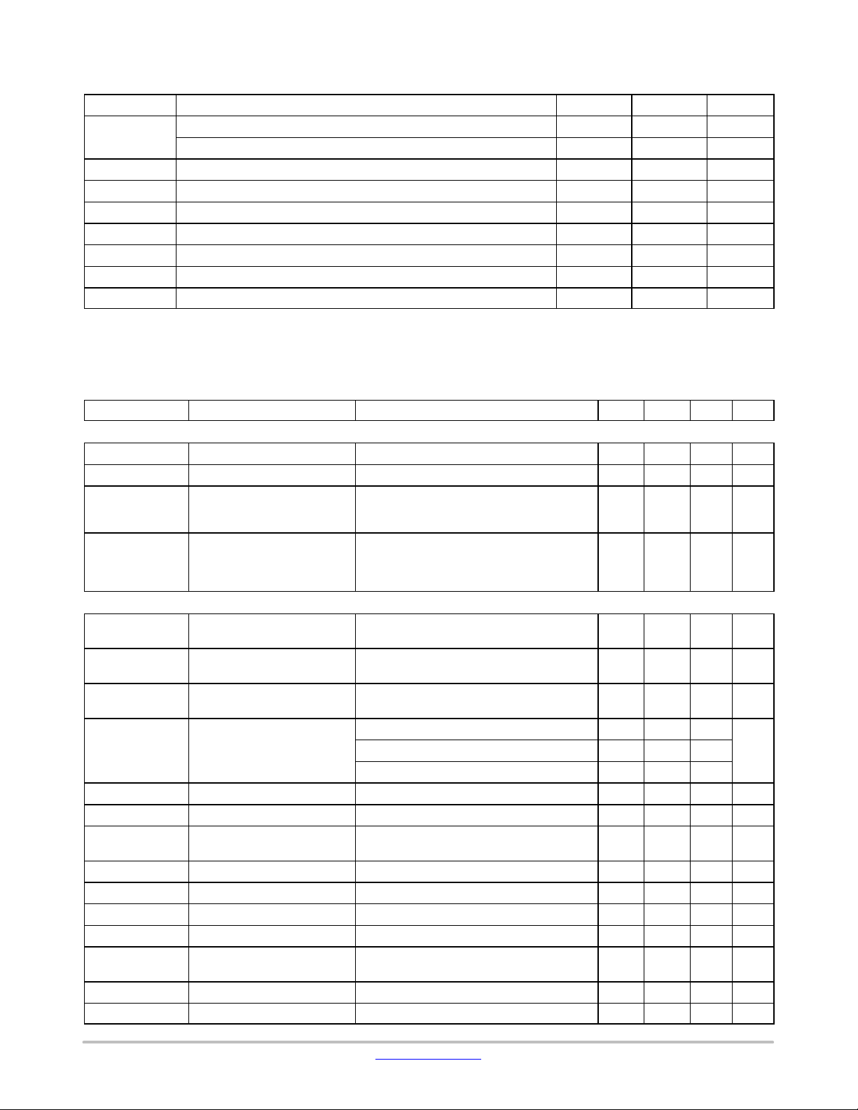
ISO11898−2:2016 PARAMETER CROSS−REFERENCE TABLE
ISO 11898−2:2016 Specification NCV7451 Datasheet
Parameter Notation Symbol
DOMINANT OUTPUT CHARACTERISTICS
Single ended voltage on CAN_H
Single ended voltage on CAN_L V
Differential voltage on normal bus load V
Differential voltage on effective resistance during arbitration V
Differential voltage on extended bus load range (optional) V
DRIVER SYMMETRY
Driver symmetry
DRIVER OUTPUT CURRENT
Absolute current on CAN_H
Absolute current on CAN_L I
RECEIVER OUTPUT CHARACTERISTICS, BUS BIASING ACTIVE
Single ended output voltage on CAN_H
Single ended output voltage on CAN_L V
Differential output voltage V
RECEIVER OUTPUT CHARACTERISTICS, BUS BIASING INACTIVE
Single ended output voltage on CAN_H
Single ended output voltage on CAN_L V
Differential output voltage V
TRANSMIT DOMINANT TIMEOUT
Transmit dominant timeout, long
Transmit dominant timeout, short t
STATIC RECEIVER INPUT CHARACTERISTICS, BUS BIASING ACTIVE
Recessive state differential input voltage range
Dominant state differential input voltage range V
STATIC RECEIVER INPUT CHARACTERISTICS, BUS BIASING INACTIVE
Recessive state differential input voltage range
Dominant state differential input voltage range V
RECEIVER INPUT RESISTANCE
Differential internal resistance
Single ended internal resistance R
RECEIVER INPUT RESISTANCE MATCHING
Matching a of internal resistance
IMPLEMENTATION LOOP DELAY REQUIREMENT
Loop delay
DATA SIGNAL TIMING REQUIREMENTS for use with bit rates above 1 Mbit/s and up to 2 Mbit/s
Transmitted recessive bit width @ 2 Mbit/s
Received recessive bit width @ 2 Mbit/s t
Receiver timing symmetry @ 2 Mbit/s
V
I
V
V
R
t
Bit(RXD)
CAN_H
CAN_L
Diff
Diff
Diff
V
SYM
CAN_H
CAN_L
CAN_H
CAN_L
Diff
CAN_H
CAN_L
Diff
t
dom
dom
V
Diff
Diff
V
Diff
Diff
R
Diff
CAN_H
CAN_L
m
R
t
Loop
Bit(Bus)
Dt
Rec
V
o(dom)(CANH)
V
o(dom)(CANL)
V
o(dom)(diff)
V
o(dom)(diff)_arb
NA
V
o(sym)
I
o(SC)(CANH)
I
o(SC)(CANL)
V
o(rec)(CANH)
V
o(rec)(CANL)
V
o(rec)(diff)
V
o(off)(CANH)
V
o(off)(CANL)
V
o(off)(dif)
t
dom(TxDC)
NA
V
i(rec)(diff)_NM
V
i(dom)(diff)_NM
V
i(rec)(diff)_LP
V
i(dom)(diff)_LP
R
i(diff)
R
i(cm)(CANH)
R
i(cm)(CANL)
R
i(cm)(m)
t
pd_rd
t
pd_dr
t
Bit(Vi(diff))
t
Bit(RxDC)
Dt
Rec
www.onsemi.com
15
Page 16

NCV7451
ISO11898−2:2016 PARAMETER CROSS−REFERENCE TABLE (continued)
ISO 11898−2:2016 Specification NCV7451 Datasheet
Parameter SymbolNotation
DATA SIGNAL TIMING REQUIREMENTS for use with bit rates above 2 Mbit/s and up to 5 Mbit/s
Transmitted recessive bit width @ 5 Mbit/s
Transmitted recessive bit width @ 5 Mbit/s t
Received recessive bit width @ 5 Mbit/s
MAXIMUM RATINGS OF V
Maximum rating V
Diff
General maximum rating V
CAN_H
CAN_H
, V
and V
Optional: Extended maximum rating V
CAN_L
CAN_L
CAN_H
AND V
and V
DIFF
CAN_L
MAXIMUM LEAKAGE CURRENTS ON CAN_H AND CAN_L, UNPOWERED
Leakage current on CAN_H, CAN_L
BUS BIASING CONTROL TIMINGS
CAN activity filter time, long
CAN activity filter time, short t
Optional: Wake−up timeout, short t
Optional: Wake−up timeout, long t
Timeout for bus inactivity (Required for selective wake−up implementation only) t
Bus Bias reaction time (Required for selective wake−up implementation only) t
t
Bit(RXD)
V
V
V
V
I
CAN_H
I
Bit(Bus)
Dt
Rec
V
Diff
CAN_H
CAN_L
CAN_H
CAN_L
CAN_L
t
Filter
Filter
Wake
Wake
Silence
Bias
t
Bit(Vi(diff))
t
Bit(RxDC)
Dt
Rec
Vdiff
CANH
CANL
NA
,
I
LI
NA
t
wake_filt
NA
t
wake_to
NA
NA
www.onsemi.com
16
Page 17

PIN ONE
REFERENCE
0.08
NOTE 4
C0.10
C
C
C
DETAIL A
1
D
TOP VIEW
DETAIL B
SIDE VIEW
D2
NCV7451
PACKAGE DIMENSIONS
DFNW14 4.5x3, 0.65P
CASE 507AC
ISSUE D
NOTES:
A B
LL
ALTERNATE
E
DETAIL A
CONSTRUCTION
EXPOSED
COPPER
A
A1
PLATING
A4
DETAIL B
C
SEATING
PLANE
14X
L
PLATED
SURFACES
A4
L3
A3
7
SECTION C−C
L3L3
1. DIMENSIONS AND TOLERANCING PER
ASME Y14.5M, 1994.
2. CONTROLLING DIMENSION: MILLIMETERS.
3. DIMESNION b APPLIES TO PLATED
TERMINAL AND IS MEASURED BETWEEN
0.15 AND 0.30 MM FROM TERMINAL.
4. COPLANARITY APPLIES TO THE EXPOSED
PAD AS WELL AS THE TERMINALS.
5. THIS DEVICE CONTAINS WETTABLE FLANK
DESIGN FEATURES TO AID IN FILLET FORMATION ON THE LEADS DURING MOUNTING.
MILLIMETERS
DIM MIN NOM
A 0.80 0.85
A1 −−− −−−
A3
A4
0.10 −−− −−−
b 0.25 0.30
D
4.40 4.50
D2 4.13 4.20
E
2.90 3.00
E2 1.53 1.60
e 0.65 BSC
K
L 0.35 0.40
L3
0.00 0.05 0.10
0.20 REF
0.30 REF
MAX
0.90
0.05
0.35
4.60
4.27
3.10
1.67
0.45
E2
14
K
e
BOTTOM VIEW
8
b
14X
M
C AB
0.10
M
NOTE 3
C
0.05
3.60
RECOMMENDED
SOLDERING FOOTPRINT*
4.35
4.23
1.75
14
1
0.65
PITCH
14X
0.33
DIMENSIONS: MILLIMETERS
8
7
14X
0.75
PACKAGE
OUTLINE
*For additional information on our Pb−Free strategy and soldering
details, please download the ON Semiconductor Soldering and
Mounting Techniques Reference Manual, SOLDERRM/D.
www.onsemi.com
17
Page 18

NCV7451
ON Semiconductor and are trademarks of Semiconductor Components Industries, LLC dba ON Semiconductor or its subsidiaries in the United States and/or other countries.
ON Semiconductor owns the rights to a number of patents, trademarks, copyrights, trade secrets, and other intellectual property. A listing of ON Semiconductor ’s product/patent
coverage may be accessed at www.onsemi.com/site/pdf/Patent−Marking.pdf
ON Semiconductor makes no warranty, representation or guarantee regarding the suitability of its products for any particular purpose, nor does ON Semiconductor assume any liability
arising out of the application or use of any product or circuit, and specifically disclaims any and all liability, including without limitation special, consequential or incidental damages.
Buyer is responsible for its products and applications using ON Semiconductor products, including compliance with all laws, regulations and safety requirements or standards,
regardless of any support or applications information provided by ON Semiconductor. “Typical” parameters which may be provided in ON Semiconductor data sheets and/or
specifications can and do vary in different applications and actual performance may vary over time. All operating parameters, including “Typicals” must be validated for each customer
application by customer’s technical experts. ON Semiconductor does not convey any license under its patent rights nor the rights of others. ON Semiconductor products are not
designed, intended, or authorized for use as a critical component in life support systems or any FDA Class 3 medical devices or medical devices with a same or similar classification
in a foreign jurisdiction or any devices intended for implantation in the human body. Should Buyer purchase or use ON Semiconductor products for any such unintended or unauthorized
application, Buyer shall indemnify and hold ON Semiconductor and its officers, employees, subsidiaries, affiliates, and distributors harmless against all claims, costs, damages, and
expenses, and reasonable attorney fees arising out of, directly or indirectly, any claim of personal injury or death associated with such unintended or unauthorized use, even if such
claim alleges that ON Semiconductor was negligent regarding the design or manufacture of the part. ON Semiconductor is an Equal Opportunity/Affirmative Action Employer. This
literature is subject to all applicable copyright laws and is not for resale in any manner.
. ON Semiconductor reserves the right to make changes without further notice to any products herein.
PUBLICATION ORDERING INFORMATION
LITERATURE FULFILLMENT:
Email Requests to: orderlit@onsemi.com
ON Semiconductor Website: www.onsemi.com
◊
TECHNICAL SUPPORT
North American Technical Support:
Voice Mail: 1 800−282−9855 Toll Free USA/Canada
Phone: 011 421 33 790 2910
www.onsemi.com
Europe, Middle East and Africa Technical Support:
Phone: 00421 33 790 2910
For additional information, please contact your local Sales Representative
18
 Loading...