

Page 1

NCV7425EVB
NCV7425 LIN Transceiver
with Voltage Regulator and
Reset Pin Evaluation Board
User's Manual
http://onsemi.com
EVAL BOARD USER’S MANUAL
Introduction
This document describes the NCV7425EVB board for the
ON Semiconductor NCV7425 LIN Transceiver with
Voltage Regulator and Reset pin. The functionality and
major parameters can be evaluated with the NCV7425EVB
board.
The NCV7425 is a fully featured local interconnect
network (LIN) transceiver designed to interface between a
LIN protocol controller and the physical bus.
The NCV7425 LIN device is a member of the in-vehicle
networking (IVN) transceiver family of ON Semiconductor
that integrates a LIN v2.1 physical transceiver and a
low-drop voltage regulator. It is designed to work in harsh
automotive environment and is submitted to the TS16949
qualification flow.
Evaluation Board Features
One-row Pin Header Connecting to all Circuit Signals
Enables Easy Insertion of the Evaluation Board into a
more Complex Application Setup. The Header can be
Alternatively Assembled either Perpendicular or
Parallel with the Board Plane
Oscilloscope Test-points on All Circuit Signals
Reverse Protection and Decoupling on the Main
(Battery) Supply
Decoupling on VCC Regulator Output
Additional Pull-up Resistor on the RSTN Open-drain
Output
Filtering Circuit on the Switch-monitoring WAKE
Input
On-board Local Wakeup Switch
LIN-bus Termination and Optional ESD Protection
Good Thermal Connection of the Circuit’s Exposed Pad
to the Bottom Ground Plane
NCV7425 Key Features
LIN-Bus Transceiver
LIN Compliant to Specification Revision 2.1
(Backward Compatible to Versions 2.0 and 1.3)
and SAE J2602
Bus Voltage 45 V
Transmission Rate up to 20 kBaud
Integrated Slope Control for Improved EMI
Compatibility
Protection
Thermal Shutdown
Indefinite Short-circuit Protection on Pins LIN
and WAKE Towards Supply and Ground
Load Dump Protection (45 V)
Bus Pins Protected against Transients in an
Automotive Environment
ESD Protection Level for LIN, INH, WAKE and
Vbb up to 10 kV
Voltage Regulator
Two Device Versions: Output Voltage 3.3 V or 5 V
for Loads up to 150 mA
Under-voltage Detector with a Reset Output to the
Supplied Microcontroller
Over-current Limitation
INH Output for Auxiliary Purposes (Switching of an
External Pull-up or Resistive Divider towards
Battery, Control of an External Voltage Regulator
etc.)
Typical Applications
Automotive
Industrial Network
Semiconductor Components Industries, LLC, 2011
November, 2011 − Rev. 0
1 Publication Order Number:
EVBUM2045/D
Page 2
NCV7425EVB
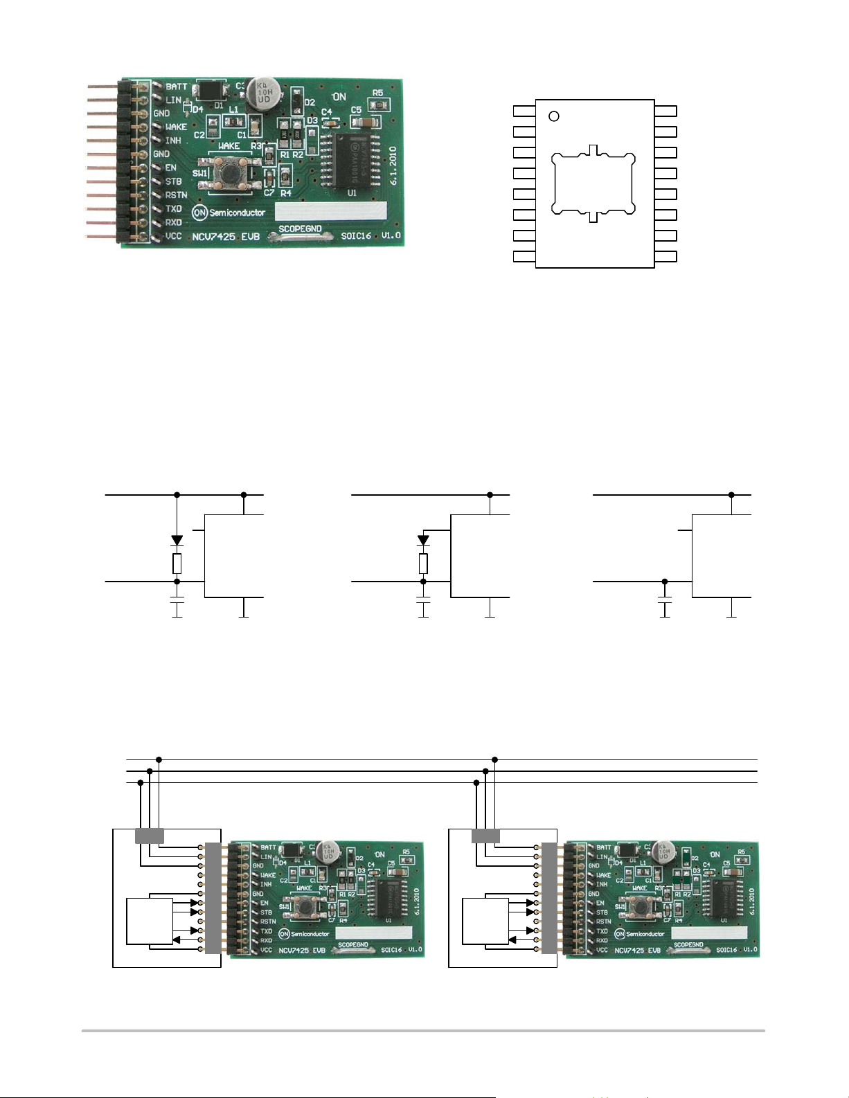
NCV7425 PIN CONNECTIONS
Figure 1. NCV7425EVB
Getting Started
Master/Slave Configuration
The NCV7425 evaluation board can be configured as
Master or Slave node. Furthermore, Master node LIN bus
pull-up resistance (R
) can be tied to VBB supply line or
LIN
to INH pin (See the figures below).
VBB
VBB
V
BB
LIN
GND
GND
WAKE
INH
OTP_SUP
N.C.
1
2
3
4
5
6
710
89
SOIC−16 LEAD
WIDE BODY
EXPOSED PAD
CASE 751AG
NCV7425
16
15
14
13
12
11
V
CC
RxD
TxD
RSTN
STB
EN
TEST
N.C.
The EMC immunity of the Master-node device can be
further enhanced by adding a capacitor between the LIN
output and ground (C
). The optimum value of this
LIN
capacitor is determined by the length and capacitance of the
LIN bus, the number and capacitance of Slave devices, the
pull-up resistance of all devices (Master and Slave), and the
required time constant of the system.
VBB
LIN Bus
VBB
INH
R
LIN
C
LIN
NCV7425
LIN
LIN Bus
R
LIN
C
LIN
INH
NCV7425
LIN
VBB
LIN Bus
VBB
INH
NCV7425
LIN
C
LIN
Figure 2. Master with Pull-up to VBB Figure 3. Master with Pull-up to INH Figure 4. Slave Configuration
Basic Connection
A simple LIN network configuration is shown in the
figure below. One Master and one Slave node is required
(Master/Slave Configuration).
VBAT
LIN
GND
GND
MCU
VCC
MASTER Node
MASTER
GND
MCU
VCC
SLAVE Node
SLAVE
Figure 5. NCV7425 Evaluation Setup Connection
http://onsemi.com
2
Page 3

NCV7425EVB
Functional Description
The junction temperature is monitored via a thermal
shutdown circuit that switches the LIN transmitter and
Overall Functional Description
NCV7425 is designed as a master or slave node for the
LIN communication interface with an integrated 3.3 V or
5 V voltage regulator having a current capability up to
150 mA for supplying any external components
(microcontroller, CAN node, etc.).
NCV7425 contains the LIN transmitter, LIN receiver,
voltage regulator, power-on-reset (POR) circuits and
thermal shutdown (TSD). The LIN transmitter is optimized
for the maximum specified transmission speed of 20 kBaud
with EMC performance due to reduced slew rate of the LIN
voltage regulator off when temperature exceeds the TSD
trigger level.
NCV7425 has four operating states (normal mode, low
slope mode, stand-by mode, and sleep mode) that are
determined by the input signals EN, WAKE, STB, and TxD.
Operating States
NCV7425 provides four operating states, two modes for
normal operation with communication, one stand-by
without communication and one low power mode with very
low current consumption - see Figure 6 and Table 1.
output.
Table 1. MODE SELECTION
LIN
Mode Vcc RxD INH
Normal – Slope
(Note 1)
ON Low = Dominant State
High = Recessive State
High if STB = High
during State Transition;
Transceiver
Normal Slope ON High
Floating Otherwise
Normal – Low Slope
(Note 2)
ON Low = Dominant State
High = Recessive State
High if STB = High
during State Transition;
Low Slope ON High
Floating Otherwise
Stand-by (Note 3) ON Low after LIN Wakeup,
Floating OFF OFF Controlled by VCC
High Otherwise (Note 4)
Sleep OFF Clamped to Vcc (Note 4) Floating OFF OFF Low
1. The normal slope mode is entered when pin EN goes HIGH while TxD is in HIGH state during EN transition.
2. The low slope mode is entered when pin EN goes HIGH while TxD is in LOW state during EN transition. LIN transmitter gets on only after
TxD returns to high after the state transition.
3. The stand-by mode is entered automatically after power-up.
4. In Stand-by and Sleep mode, the High state is achieved by internal pull-up resistor to VCC.
30 kW
on LIN
RSTN
Under-voltage
Monitor
Normal Mode
(Normal Slope)
: On
− V
CC
− LIN TRX: On
− INH: High/Floating
− LIN Term.: 30 kW
− RxD Pin: LIN Data
− RSTN Pin: High
EN Changes 1 −> 0 while STB = 0
Sleep Mode
− VCC: Off
− LIN TRX: Off
− INH: Floating
− LIN Term.: Current Source
− RxD Pin: at VCC
− RSTN Pin: Low
PD20090610.01
Vbb Power-up
Standby Mode
− VCC: On
− LIN TRX: Off
− INH: Floating
− LIN Term.: Current Source
− RxD Pin: High/Low
− RSTN Pin: VCC_UV
VCC Under-voltage
EN Changes 0 −> 1 while TxD = 0
EN Changes 1 −> 0 while STB = 1
Normal Mode
(Low Slope)
− VCC: On
− LIN TRX: On
− INH: High/Floating
− LIN Term.: 30 kW
− RxD Pin: LIN Data
− RSTN Pin: High
EN Changes 0 −> 1 while TxD = 1
EN Changes 1 −> 0 while STB = 1
VCC Under-voltage
LIN or Local Wake-up
EN Changes 1 −> 0 while STB = 0
Figure 6. NCV7425 State Diagram
Additional details of the NCV7425 operation and parameters can be found in the corresponding datasheet [1].
http://onsemi.com
3
Page 4

NCV7425EVB
Schematic
Figure 7. NCV7425 LIN Transceiver with Voltage Regulator and Reset Pin Evaluation Board Schematic
Bill of Materials
Table 2. NCV7425 Evaluation Board Bill of Materials
Designator Description Value Footprint Manufacturer
C1 Capacitor SMD 1.0 nF CAP0805 PHYCOMP 2238 580 15623
R1, R2 Resistor SMD
R3, R5 Resistor SMD
C7 Capacitor SMD 10 nF CAP0603 EPCOS B37931K5103K60
C5 Capacitor SMD X7R
C3 Electrolytic Capacitor SMD
R4 Resistor SMD
C4 Capacitor SMD 100 nF CAP0603 KEMET C0603C104K5RAC
C2 Capacitor SMD (Optional) (Optional) CAP0805 (Optional) (Optional)
D1 Diode SMD MRA4003 SMA ON Semiconductor MRA4003T3G
D4 LIN bus ESD protection diode ESD LIN SOD323 (Optional) (Optional)
L1
J1
D2, D3 Switching Diode SMD MMSD4148 SOD123 ON Semiconductor MMSD4148T1G
U1
SCOPEGND SCOPEGND; Wire Bridge SCOPEGND SCOPEGND - -
SW1
FT1, FT2, FT3,
FT4
TP1, TP2, TP4,
TP5, TP7, TP8,
TP9, TP10,
TP11, TP12
Resistor SMD
(Optional Ferrite)
SIL HEADER 12 pins
Right Angle
LIN Transceiver with 3.3 V
or 5 V Voltage Regulator
SWITCH SMD SPNO
6x6mm
Rubber feet
12,7 x 12,7 x 5,8
Testpin 200 SER.
Hole 1.0 Black
2.0 kW 1206
0.25 W
10 kW
10 mF 10 V X7R
10 mF 50 V
33 kW
0R R0805 MULTICOMP MC 0.1W 0805 0R
HEADER 1X12 HDR1x12 MOLEX 90121-0772
NCV7425
SMD SWITCH PB300
SUPPORT FEET
TP S200 H1.0
BLACK
R1206 WELWYN WCR 1206 2K 2%
R0805 MULTICOMP MC 0.1 W 0805 1% 10K
CAP1206 KEMET C1206C106K8RAC
6.3 x 6.3 SMD NICHICON UUD1H100MCL1GS
R0805 MULTICOMP MC 0.1 W 0805 1% 33K
SOIC16_WB_
EP
FEET
12,7 x 12,7
TESTPIN2 VERO 20-2137
ON Semiconductor
TYCO
ELECTRONICS
3M SJ5018BLACK
Manufacturer Part
Number
3.3 V: NCV7425DW0R2G
5 V: NCV7425DW5R2G
FSM2JSMA
http://onsemi.com
4
Page 5

PCB Drawings
Assembly Drawings
NCV7425EVB
Figure 8. NCV7425EVB PCB
Top Assembly Drawing
Composite Drawings
Figure 10. NCV7425EVB PCB
Top Composite Drawing
PCB Preview
Figure 9. NCV7425EVB PCB
Bottom Assembly Drawing
Figure 11. NCV7425EVB PCB
Bottom Composite Drawing (Mirrored)
Figure 12. NCV7425EVB PCB Top Side View Figure 13. NCV7425EVB PCB Bottom Side View
http://onsemi.com
5
Page 6

NCV7425EVB
References
[1] On Semiconductor, NCV7425 Product Preview Revision P0, August 2011.
ON Semiconductor and are registered trademarks of Semiconductor Components Industries, LLC (SCILLC). SCILLC reserves the right to make changes without further notice
to any products herein. SCILLC makes no warranty, representation or guarantee regarding the suitability of its products for any particular purpose, nor does SCILLC assume any liability
arising out of the application or use of any product or circuit, and specifically disclaims any and all liability, including without limitation special, consequential or incidental damages.
“Typical” parameters which may be provided in SCILLC data sheets and/or specifications can and do vary in different applications and actual performance may vary over time. All
operating parameters, including “Typicals” must be validated for each customer application by customer’s technical experts. SCILLC does not convey any license under its patent rights
nor the rights of others. SCILLC products are not designed, intended, or authorized for use as components in systems intended for surgical implant into the body, or other applications
intended to support or sustain life, or for any other application in which the failure of the SCILLC product could create a situation where personal injury or death may occur. Should
Buyer purchase or use SCILLC products for any such unintended or unauthorized application, Buyer shall indemnify and hold SCILLC and its officers, employees, subsidiaries, affiliates,
and distributors harmless against all claims, costs, damages, and expenses, and reasonable attorney fees arising out of, directly or indirectly, any claim of personal injury or death
associated with such unintended or unauthorized use, even if such claim alleges that SCILLC was negligent regarding the design or manufacture of the part. SCILLC is an Equal
Opportunity/Affirmative Action Employer. This literature is subject to all applicable copyright laws and is not for resale in any manner.
PUBLICATION ORDERING INFORMATION
LITERATURE FULFILLMENT:
Literature Distribution Center for ON Semiconductor
P.O. Box 5163, Denver, Colorado 80217 USA
Phone: 303−675−2175 or 800−344−3860 Toll Free USA/Canada
Fax: 303−675−2176 or 800−344−3867 Toll Free USA/Canada
Email: orderlit@onsemi.com
N. American Technical Support: 800−282−9855 Toll Free
USA/Canada
Europe, Middle East and Africa Technical Support:
Phone: 421 33 790 2910
Japan Customer Focus Center
Phone: 81−3−5817−1050
http://onsemi.com
ON Semiconductor Website: www.onsemi.com
Order Literature: http://www.onsemi.com/orderlit
For additional information, please contact your local
Sales Representative
EVBUM2045/D
6
 Loading...