

Page 1
NCV7329
f
Stand-alone LIN Transceiver
Description
The NCV7329 is a fully featured local interconnect network (LIN)
transceiver designed to interface between a LIN protocol controller
and the physical bus.
The LIN bus is designed to communicate low rate data from control
devices such as door locks, mirrors, car seats, and sunroofs at the
lowest possible cost. The bus is designed to eliminate as much wiring
as possible and is implemented using a single wire in each node. Each
node has a slave MCU−state machine that recognizes and translates
the instructions specific to that function.
The main attraction of the LIN bus is that all the functions are not
time critical and usually relate to passenger comfort.
Features
• LIN−Bus Transceiver
♦ Compliant to ISO 17987−4 (Backwards Compatible to LIN
Specification rev. 2.x, 1.3) and SAE J2602
♦ Bus Voltage $42 V
♦ Transmission Rate 1 kbps to 20 kbps
♦ TxD Timeout Function
♦ Integrated Slope Control
• Protection
♦ Thermal Shutdown
♦ Undervoltage Protection
♦ Bus Pins Protected Against Transients in an Automotive
Environment
• Modes
♦ Normal Mode: LIN Transceiver Enabled, Communication via the
Bus is Possible
♦ Sleep Mode: LIN Transceiver Disabled, the Consumption from
is Minimized
V
BB
♦ Standby Mode: Transition Mode Reached after Wake−up Event o n
the LIN Bus
• Compatibility
♦ Pin−Compatible Subset with NCV7321
♦ K−line Compatible
Quality
• NCV Prefix for Automotive and Other Applications Requiring
Unique Site and Control Change Require− ments; AEC−Q100
Qualified and PPAP Capable
• These Devices are Pb−Free, Halogen Free/BFR Free and are RoHS
Compliant
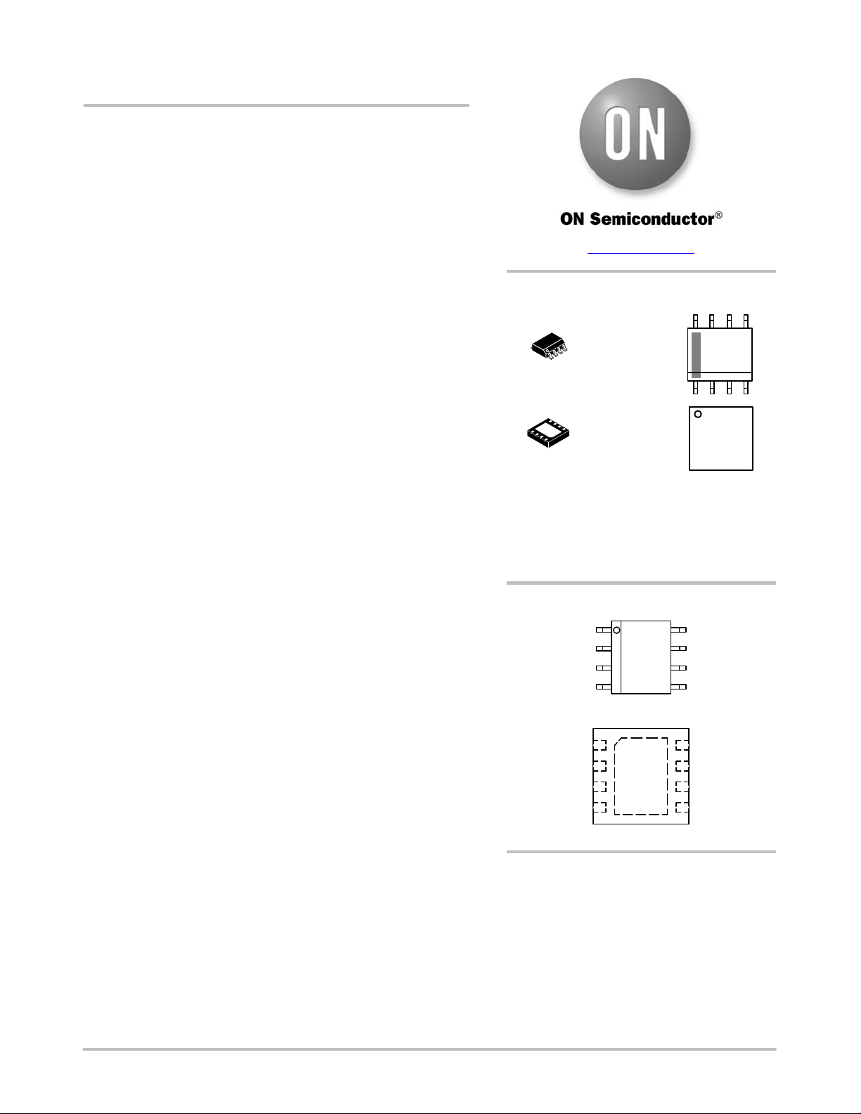
www.onsemi.com
MARKING
DIAGRAMS
8
8
1
1
(Note: Microdot may be in either location)
SOIC−8
CASE 751AZ
DFN8
CASE 507AB
A = Assembly Location
L = Wafer Lot
Y = Year
W = Work Week
G = Pb−Free Package
1
1
NV7329
ALYW
G
NV73
29
ALYWG
G
PIN CONNECTIONS
EP
81
NC
7
V
BB
6
LIN
5
GND
NC
81
V
7
BB
LIN
6
5
GND
RxD
2
EN
3
NC
4
TxD
SOIC−8 (Top View)
RxD
EN
2
3
NC
4
TxD
DFN8 (Top View)
ORDERING INFORMATION
See detailed ordering and shipping information on page 10 o
this data sheet.
© Semiconductor Components Industries, LLC, 2018
May, 2018 − Rev. 0
1 Publication Order Number:
NCV7329/D
Page 2
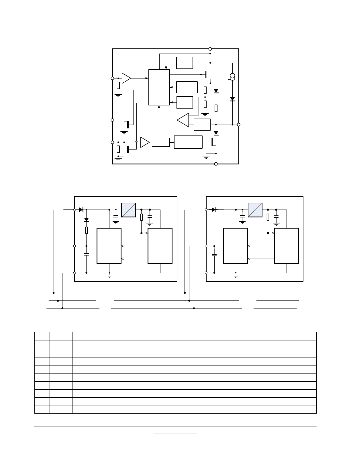
EN
RxD
NCV7329
BLOCK DIAGRAM
POR
State
Control
COMP
Thermal
shutdown
Osc
+
−
Filter
V
BB
I
sleep
D
S
R
SLAVE
LIN
VBAT
LIN
GND
1 kΩ
1 nF
TxD
time−out
Slope Control
NCV7329
Figure 1. Block Diagram
TYPICAL APPLICATION
bat
3.3/5V
10 μF
V
BB
RxD
7
LIN
8
6
3
LIN−BUS
KL30
KL31
NCV7329
5
GND
1
TxD
4
EN
2
Figure 2. Typical Application Diagram for a Master Node
Master Node
10 kΩ
100 nF
LB20140619.0
VCC
Microcontroller
GND
VBAT
LIN
GND
GND
220 pF
LIN
bat
Slave Node
3.3/5V
10 μF
V
BB
7
8
6
3
NCV7329
5
GND
KL30
LIN−BUS
KL31
1
4
2
RxD
TxD
EN
10 kΩ
100 nF
VCC
Microcontroller
GND
LB20140619.0
Table 1. PIN DESCRIPTION
Pin Name Description
1 RxD Receive Data Output; Low in Dominant State; Open−Drain Output
2 EN Enable Input, Transceiver in Normal Operation Mode when High, Pull−down Resistor to GND
3 NC Not Connected
4 TxD Transmit Data Input, Low for Dominant State, Pull−down to GND
5 GND Ground
6 LIN LIN Bus Output/Input
7 V
Battery Supply Input
BB
8 NC Not Connected
− EP Exposed Pad. Recommended to connect to GND or left floating in application (DFN8 package only).
www.onsemi.com
2
Page 3
NCV7329
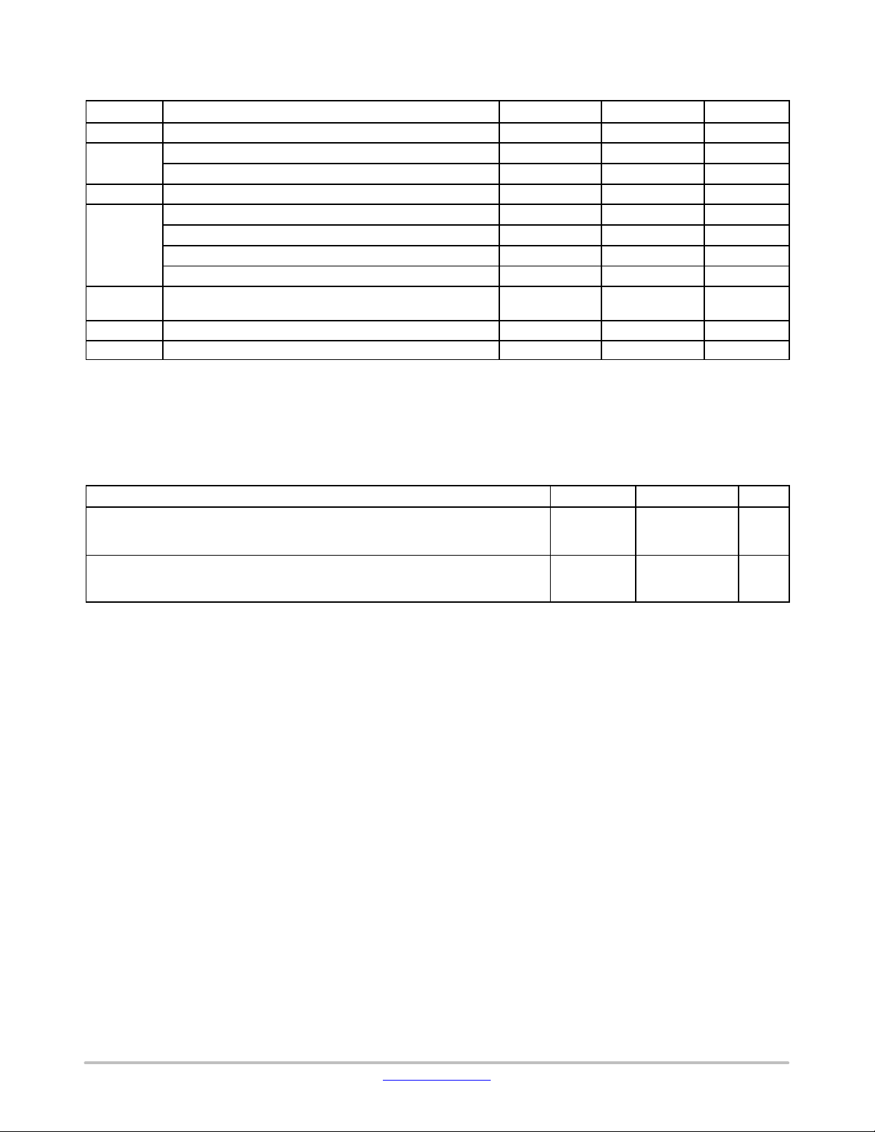
Table 2. ABSOLUTE MAXIMUM RATINGS
Symbol Parameter Min Max Unit
V
BB
V
LIN
V_Dig_IO DC Input Voltage on Pins (EN, RxD, TxD) −0.3 +7 V
V
ESD
V
ESDIEC
T
J
T
STG
Stresses exceeding those listed in the Maximum Ratings table may damage the device. If any of these limits are exceeded, device functionality
should not be assumed, damage may occur and reliability may be affected.
1. Standardized human body model electrostatic discharge (ESD) pulses in accordance to EIA−JESD22. Equivalent to discharging a 100 pF
capacitor through a 1.5 kW resistor.
2. Standardized charged device model ESD pulses when tested according to AEC−Q100−011.
3. In accordance to JEDEC JESD22−A115. Equivalent to discharging a 200 pF capacitor through a 10 W resistor and 0.75 mH coil.
4. Equivalent to discharging a 150 pF capacitor through a 330 W resistor. System HBM levels are verified by an external test−house.
Voltage on Pin V
BB
−0.3 +42 V
LIN Bus Voltage with respect to GND −42 +42 V
LIN Bus Voltage with respect to V
BB
−42 +42 V
Human Body Model (LIN Pin) (Note 1) −8 +8 kV
Human Body Model (All Pins) (Note 1) −4 +4 kV
Charged Device Model (All Pins) (Note 2) −750 +750 V
Machine Model (All Pins) (Note 3) −200 +200 V
Electrostatic Discharge Voltage (LIN Pin) System Human Body
−8 +8 kV
Model (Note 4) Conform to IEC 61000−4−2
Junction Temperature Range −40 +150 °C
Storage Temperature Range −55 +150 °C
Table 3. THERMAL CHARACTERISTICS
Parameter Symbol Value Unit
Thermal characteristics, SOIC−8 (Note 5)
Thermal characteristics, DFN8 (Note 5)
5. Refer to ELECTRICAL CHARACTERISTICS, RECOMMENDED OPERATING RANGES and/or APPLICATION INFORMATION for Safe
Operating parameters.
6. Values based on test board according to EIA/JEDEC Standard JESD51−3, signal layer with 10% trace coverage.
7. Values based on test board according to EIA/JEDEC Standard JESD51−7, signal layers with 10% trace coverage.
Thermal Resistance Junction−to−Air, Free air, 1S0P PCB (Note 6)
Thermal Resistance Junction−to−Air, Free air, 2S2P PCB (Note 7)
Thermal Resistance Junction−to−Air, Free air, 1S0P PCB (Note 6)
Thermal Resistance Junction−to−Air, Free air, 2S2P PCB (Note 7)
R
q
JA
R
q
JA
R
q
JA
R
q
JA
131
81
125
58
°C/W
°C/W
°C/W
°C/W
www.onsemi.com
3
Page 4
NCV7329
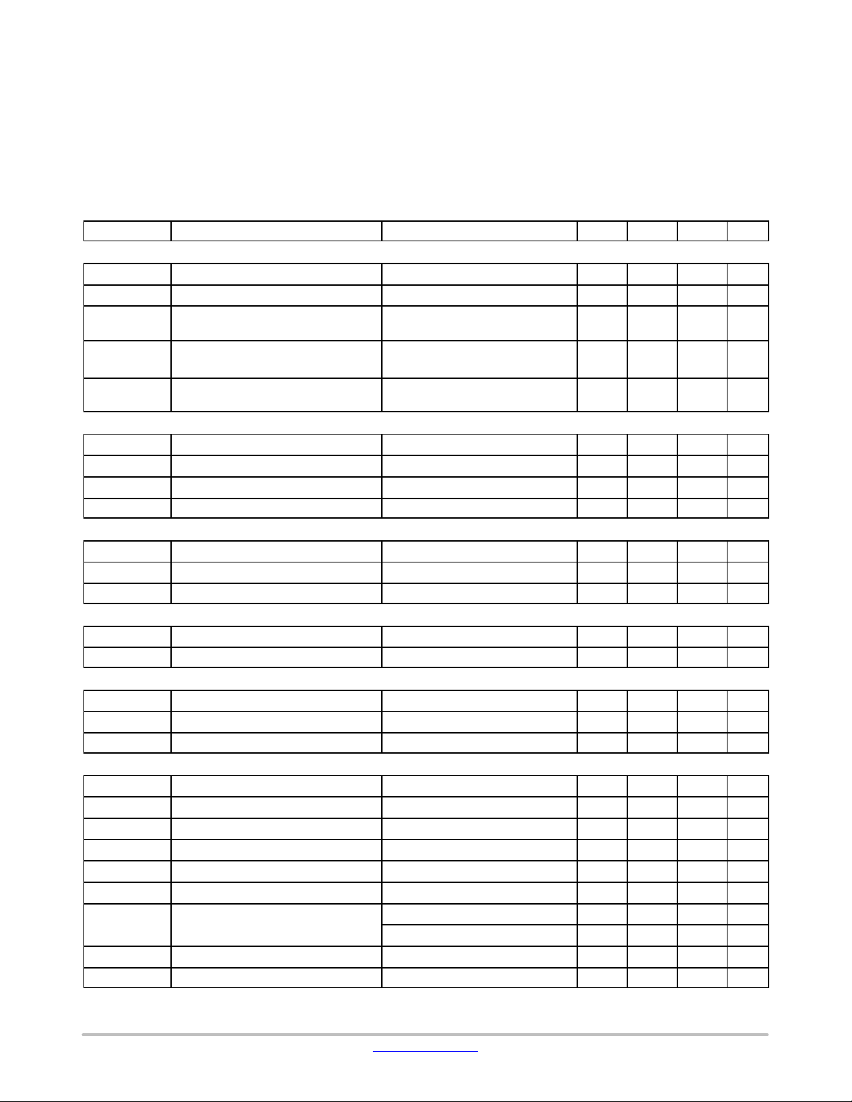
ELECTRICAL CHARACTERISTICS
Definitions
All voltages are referenced to GND (pin 5) unless otherwise specified. Positive currents flow into the IC. Sinking current means
the current is flowing into the pin; sourcing current means the current is flowing out of the pin.
Table 4. DC CHARACTERISTICS (V
Bus Load = 500 W (V
Symbol
to LIN); unless otherwise specified.)
BB
Parameter Conditions Min. Typ. Max. Unit
= 5 V to 18 V; TJ = −40°C to +150°C; Typical values are given at VBB = 12 V and TJ = 25°C
BB
SUPPY PIN (VBB)
V
BB
I
BB
I
BB
I
BB
Battery Supply 5 18 V
Battery Supply Current Normal Mode; LIN recessive 0.2 0.55 1.2 mA
Battery Supply Current Normal Mode; TxD = Low, LIN
Dominant
Battery Supply Current Sleep and Standby Mode;
LIN recessive;
I
BB
Battery Supply Current Sleep and Standby Mode;
LIN recessive;
POR AND VBB MONITOR
PORH_V
PORL_V
MONH_V
MONL_V
BB
BB
BB
Power−on Reset; High Level on V
Power−on Reset; Low Level on V
Battery Monitoring High Level VBB Rising 3.2 4.2 5.0 V
BB
BB
BB
Battery Monitoring Low Level VBB Falling 3.0 4.0 4.8 V
VBB Rising 2.7 3.5 4.4 V
VBB Falling 1.3 2.1 2.7 V
TRANSMITTER DATA INPUT (PIN TxD)
V
IL_TxD
V
IH_TxD
R
PD_TxD
Low Level Input Voltage −0.3 +0.8 V
High Level Input Voltage 2 7 V
Pull−down Resistor on TxD Pin 50 125 325
RECEIVER DATA OUTPUT (PIN RxD)
I
OL_RxD
I
OH_RxD
Low Level Output Current V
High Level Output Current −5 +5
= 0.4 V 2 mA
RXD
ENABLE INPUT (PIN EN)
V
IL_EN
V
IH_EN
R
PD_EN
Low Level Input Voltage −0.3 +0.8 V
High Level Input Voltage 2 7 V
Pull−down Resistor to Ground 100 250 650
LIN BUS LINE (PIN LIN)
V
BUS_DOM
V
BUS_REC
V
REC_DOM
V
REC_REC
V
REC_CNT
V
REC_HYS
V
LIN_DOM
Bus Voltage for Dominant State 0.4 V
Bus Voltage for Recessive State 0.6 V
Receiver Threshold LIN Bus Recessive − Dominant 0.4 0.6 V
Receiver Threshold LIN Bus Dominant – Recessive 0.4 0.6 V
Receiver Centre Voltage (V
Receiver Hysteresis (V
Dominant Output Voltage
REC_DOM
REC_REC
Normal mode; VBB = 7 V 1.2 V
Normal mode; VBB = 18 V 2.0 V
I
BUS_no_GND
I
BUS_no_VBB
Communication not Affected V
LIN Bus Remains Operational V
= GND = 12 V; 0 < V
BB
= GND = 0 V; 0 < V
BB
8. Values based on design and characterization. Not tested in production.
− V
+ V
V
LIN = VBB
V
LIN = VBB
REC_REC
REC_DOM
2 3.9 6.5 mA
6 10
; TJ<85°C
6 15
) / 2 0.475 0.500 0.525 V
) 0.050 0.175 V
< 18 V −1 +1 mA
LIN
< 18 V 5
LIN
mA
mA
kW
mA
kW
BB
BB
BB
BB
BB
BB
mA
www.onsemi.com
4
Page 5
NCV7329
Table 4. DC CHARACTERISTICS (V
= 5 V to 18 V; TJ = −40°C to +150°C; Typical values are given at VBB = 12 V and TJ = 25°C
BB
Bus Load = 500 W (VBB to LIN); unless otherwise specified.)
Symbol UnitMax.Typ.Min.ConditionsParameter
LIN BUS LINE (PIN LIN)
I
BUS_LIM
I
BUS_PAS_dom
I
sleep
I
BUS_PAS_rec
V
SERDiode
R
SLAVE
C
LIN
Current limitation for Driver Dominant State; V
Receiver Leakage current; Driver OFF TxD = High; V
Receiver Leakage current;
Sleep mode; V
see Figure 1
Receiver Leakage current; Driver OFF;
(Note 8)
TxD = High; 8 V < V
8 V < V
LIN
Voltage Drop on Serial Diode Voltage drop on D
Internal Pull−up Resistance see Figure 1 20 30 60
Capacitance on Pin LIN, (Note 8) 20 30 pF
8. Values based on design and characterization. Not tested in production.
= V
LIN
BB_MAX
= 0 V; VBB = 12 V −1 mA
LIN
= 0 V; V
LIN
< 18 V; V
BB
LIN
see Figure 1 0.4 0.7 1 V
S,
= 12 V −16 −8 −3
BB
< 18 V;
≥ V
BB
40 200 mA
20
mA
mA
kW
www.onsemi.com
5
Page 6

NCV7329
Table 5. AC CHARACTERISTICS (V
= 5 V to 18 V; TJ = −40°C to +150°C; unless otherwise specified. For the transmitter
BB
parameters, the following bus loads are considered: L1 = 1 kW / 1 nF; L2 = 660 W / 6.8 nF; L3 = 500 W / 10 nF)
Symbol
Parameter Conditions Min. Typ. Max. Unit
LIN TRANSCEIVER
D1
Duty Cycle 1 = t
(See Figure 4)
D2 Duty Cycle 2 = t
(See Figure 4)
D3 Duty Cycle 3 = t
(See Figure 4)
D4 Duty Cycle 4 = t
(See Figure 4)
t
TX_PROP_DOWN
t
TX_PROP_UP
Propagation Delay of TxD to LIN. TxD
High to Low (See Figure 7)
Propagation Delay of TxD to LIN. TxD
Low to High (See Figure 7)
BUS_REC(min)
BUS_REC(max)
BUS_REC(min)
BUS_REC(max)
/ (2xt
/ (2xt
/ (2xt
/ (2xt
BIT
BIT
BIT
BIT
)
TH
REC(max)
TH
DOM(max)
t
BIT
V
BB
)
TH
REC(min)
TH
DOM(min)
t
BIT
V
BB
)
TH
REC(max)
TH
DOM(max)
t
BIT
V
BB
)
TH
REC(min)
TH
DOM(min)
t
BIT
V
BB
= 0.744 x V
= 0.581 x V
= 50 ms
= 5 V to 18 V
= 0.422 x V
= 0.284 x V
= 50 ms
= 5 V to 18 V
= 0.778 x V
= 0.616 x V
= 96 ms
= 5 V to 18 V
= 0.389 x V
= 0.251 x V
= 96 ms
= 5 V to 18 V
BB
BB
BB
BB
BB
BB
0.396 0.500
BB
0.500 0.581
0.417 0.500
BB
0.500 0.590
LIN RECEIVER
t
RX_PD
t
RX_SYM
Propagation Delay of Receiver, Rising
and falling Edge (See Figure 5)
Propagation Delay Symmetry
R
RxD
R
RxD
= 2.4 kW; C
= 2.4 kW; C
RXD
RXD
= 20 pF
= 20 pF;
0.1 6
−2 +2
Rising edge with respect to falling edge
MODE TRANSITIONS AND TIMEOUTS
t
LIN_WAKE
t
TxD_TIMEOUT
t
INIT_NORM
Duration of LIN Dominant for Detection
of Wake−up via LIN Bus (See Figure 6)
TxD Dominant Timeout Normal Mode, TxD = Low 14 25 46 ms
Time From Rising Edge of EN pin to the
moment when the transmitter is able to
Sleep Mode 40 70 150
15 30 75
correctly transmit
t
ENABLE
t
DISABLE
t
TO_STB
Duration of EN pin in High Level State
for transition to Normal Mode
Duration of EN pin in Low Level State
for transition to Sleep Mode
Delay from LIN Bus Dominant to
Recessive Edge to Entering of Standby
11 20 55
11 20 55
Sleep Mode 5 10 40
Mode after Valid LIN Wake−up
(See Figure 6)
THERMAL SHUTDOWN
T
J(sd)
Shutdown Junction Temperature Temperature Rising 160 180 200 °C
9. Values based on design and characterization. Not tested in production.
14
14
ms
ms
ms
ms
ms
ms
ms
ms
ms
www.onsemi.com
6
Page 7

NCV7329
FUNCTIONAL DESCRIPTION
Overall Functional Description
LIN is a serial communication protocol that efficiently
supports the control of mechatronic nodes in distributed
automotive applications.
The NCV7329 contains the LIN transmitter, LIN receiver,
power−on−reset (POR) circuits and thermal shutdown
(TSD). The LIN transmitter is optimized for a maximum
specified transmission speed of 20 kbps.
Table 6. OPERATING MODES
Pin EN Mode Pin RxD LIN bus
x Unpowered Floating OFF; Floating
Low Sleep Floating OFF; Floating
Low Standby Low indicates
wake−up
High Normal LOW: dominant
HIGH: recessive
Unpowered Mode
OFF; 30 kW
ON; 30 kW
As long as VBB remains below its power−on−reset level,
the chip is kept in a safe unpowered state. The LIN
transmitter is inactive, the LIN pin is left floating and only
a weak pull−down is connected on pin TxD. Pin RxD
remains floating.
The unpowered state will be entered from any other state
when V
(PORL_V
high threshold (PORH_V
falls below its power−on−reset level
BB
). When VBB rises above the power−on−reset
BB
), the NCV7329 switches to a
BB
Sleep mode.
Normal Mode
In the Normal mode, the full functionality of the LIN
transceiver is available. The transceiver can transmit and
receive data via the LIN bus with speed up to 20 kbps. Data
according the state of TxD input are sent to the LIN bus
while pin RxD reflects the logical symbol received on the
LIN bus − high−impedant for recessive and Low for
dominant. A 30 kW resistor in series with a
reverse−protection diode is internally connected between
LIN and V
BB
pins.
The signal on pin TxD passes through a timer, which
releases the bus in case the TxD remains low for longer than
t
TxD_TIMEOUT
. It prevents the LIN bus being permanently
driven dominant and thus blocking all subsequent
communication due to a failure of the application (e.g.
software error). The transmission can continue once the
TxD returns to High logical level.
In case the junction temperature increases above the
thermal shutdown threshold (T
), e.g. due to a short of the
J(sd)
LIN wiring to the battery, the transmitter is disabled and
releases the LIN bus to recessive. Once the junction
temperature decreases back below the thermal shutdown
level, the transmission can be enabled again. However, to
avoid thermal oscillations, first a High logical level on TxD
must be encountered before the transmitter is enabled.
As required by SAE J2602, the transceiver must behave
safely below its operating range – it shall either continue to
transmit correctly (according its specification) or remain
silent (transmit a recessive state regardless of the TxD
signal). A battery monitoring circuit in NCV7329
deactivates the transmitter in the Normal mode if the V
BB
level drops below MONL_VBB. Transmission is enabled
again when V
reaches MONH_VBB. The internal logic
BB
remains in the no rm a l m o de and the reception from the LIN
line is still possible even if the battery monitor disables the
transmission. Although the specifications of the monitoring
and power−on−reset levels are overlapping, it’s ensured by
the implementation that the monitoring level never falls
below the power−on−reset level.
The Normal mode can be entered from either Standby or
Sleep mode when EN Pin is High for longer than t
ENABLE
When the transition is made from Standby mode, TxD
pull−down is set to weak and RxD is put into a
high−impedance immediately after EN becomes High
(before the expiration of t
ENABLE
filtering time). This
excludes signal conflicts between the Standby mode pin
settings and the signals required to control the chip in the
Normal mode after a local wake−up vs. High logical level on
TxD required to send a recessive symbol to the LIN bus.
Sleep Mode
Sleep mode provides extremely low current consumption.
The LIN transceiver is inactive and the battery consumption
is minimized.
This mode is entered in one of the following ways:
• After the voltage level at V
power−on−reset level (PORH_V
pin rises above its
BB
). In this case, RxD
BB
Pin remains high−impedant and the pull−down applied
on pin TxD remains weak.
• After assigning Low logical level to pin EN for longer
than t
DISABLE
Standby Mode
Standby mode is entered from the Sleep mode when a
remote wake−up event occurred. The Low level on RxD pin
indicates interrupt flag for the microcontroller.
while NCV7329 is in the Normal mode.
.
www.onsemi.com
7
Page 8

LIN, rising edge after t > t
LIN_WAKE
NCV7329
OPERATING STATES
VBB Below Reset Level
Unpowered
(VBB Below Reset Level)
− LIN Transceiver: OFF
− LIN Term: Floating
− RxD: Floating
VBB Above Reset Level
Sleep Mode
− LIN Transceiver: OFF
− LIN Term: Current Source
− RxD: Floating
EN = High for t > t
ENABLE
Standby Mode
− LIN Transceiver: OFF
− LIN Term: 30 kW pull−up
− RxD: Low
EN = Low for t > t
EN = High for t > t
ENABLE
Figure 3. State Diagram
DISABLE
Normal Mode
− LIN Transceiver: ON
− LIN Term: 30 kW pull−up
− RxD Receives LIN Data
www.onsemi.com
8
Page 9

NCV7329
MEASUREMENT SETUPS AND DEFINITIONS
TxD
t
BIT
t
BIT
50%
t
TH
TH
TH
TH
LIN
REC(max)
DOM(max)
REC(min)
DOM(min)
t
BUS_DOM(max)
t
BUS_REC(min)
Thresholds of
receiving node 1
Thresholds of
receiving node 2
t
t
BUS_DOM(min)
Figure 4. LIN Transmitter Duty Cycle
t
BUS_REC(max)
LIN
V
BB
RxD
V
BB
LIN
t
RX_PD
40% V
BB
t
RX_PD
50%
Figure 5. LIN Receiver Timing
Detection of Remote Wake−Up
t
LIN_WAKE
Sleep Mode
60% V
TO_STB
t
BB
Standby Mode
Figure 6. Remote (LIN) Wake−up Detection
60% V
40% V
BB
BB
t
t
LIN recessive level
LIN dominant level
t
www.onsemi.com
9
Page 10

NCV7329
TxD
t
BIT
t
BIT
50%
LIN
t
Vbb
60% Vbb
40% Vbb
t
tx_prop_down
t
tx_prop_up
RB20180511
t
Figure 7. LIN Transmitter Timing
DEVICE ORDERING INFORMATION
Part Number Description Temperature Range Package Shipping
NCV7329D10R2G
NCV7329MW0R2G
†For information on tape and reel specifications, including part orientation and tape sizes, please refer to our Tape and Reel Packaging
Specifications Brochure, BRD8011/D.
Stand−alone LIN Transceiver −40°C to +125°C
Stand−alone LIN Transceiver −40°C to +125°C
SOIC−8
(Pb−Free)
DFN8
(Pb−Free)
3000 / Tape & Reel
3000 / Tape & Reel
†
www.onsemi.com
10
Page 11

DFNW8 3x3, 0.65P
8
MECHANICAL CASE OUTLINE
PACKAGE DIMENSIONS
1
SCALE 2:1
A
B
L
E
A
A3
SEATING
C
PLANE
E2
PIN ONE
REFERENCE
0.05 C
0.05 C
NOTE 4
DETAIL A
8X
L
D
TOP VIEW
DETAIL B
C
C
SIDE VIEW
D2
14
CASE 507AB
ISSUE D
L3
L
DETAIL A
A1
A4
DETAIL B
PLATED
SURFACES
SECTION C−C
ALTERNATE
CONSTRUCTION
EXPOSED
COPPER
PLATING
A4
L3
DATE 03 JUL 201
NOTES:
1. DIMENSIONING AND TOLERANCING PER
L3
ASME Y14.5M, 1994.
2. CONTROLLING DIMENSION: MILLIMETERS.
3. DIMENSION b APPLIES TO PLATED TERMINAL
AND IS MEASURED BETWEEN 0.10 AND
0.20mm FROM THE TERMINAL TIP.
4. COPLANARITY APPLIES TO THE EXPOSED
PAD AS WELL AS THE TERMINALS.
5. THIS DEVICE CONTAINS WETTABLE FLANK
DESIGN FEATURES TO AID IN FILLET FORMATION ON THE LEADS DURING MOUNTING.
MILLIMETERS
DIM MIN NOM
A 0.80 0.85
A1 −−− −−−
A3 0.20 REF
A4
0.10 −−− −−−
b 0.25 0.30
2.95 3.00
D
D2 2.30 2.40
2.95 3.00
E
E2 1.50 1.60
e 0.65 BSC
K
L 0.35 0.40
L3
0.00 0.05 0.10
0.30 REF
MAX
0.90
0.05
0.35
3.05
2.50
3.05
1.70
0.45
GENERIC
MARKING DIAGRAM*
1
XXXXXX
XXXXXX
ALYWG
G
K
e/2
e
BOTTOM VIEW
DOCUMENT NUMBER:
DESCRIPTION:
58
8X
b
0.10 B
NOTE 3
0.05ACC
RECOMMENDED
SOLDERING FOOTPRINT*
2.55
2.28
8
3.30
1.76
1
0.65
PITCH
DIMENSIONS: MILLIMETERS
*For additional information on our Pb−Free strategy and soldering
details, please download the ON Semiconductor Soldering and
Mounting Techniques Reference Manual, SOLDERRM/D.
98AON14978G
Electronic versions are uncontrolled except when accessed directly from the Document Repository.
Printed versions are uncontrolled except when stamped “CONTROLLED COPY” in red.
5
4
8X
0.33
8X
0.75
PACKAGE
OUTLINE
DFNW8 3x3, 0.65P
XXXXXX = Specific Device Code
A = Assembly Location
L = Wafer Lot
Y = Year
W = Work Week
G = Pb−Free Package
(Note: Microdot may be in either location)
*This information is generic. Please refer to
device data sheet for actual part marking.
Pb−Free indicator, “G” or microdot “ G”, may
or may not be present. Some products may
not follow the Generic Marking.
PAGE 1 OF 1
ON Semiconductor and are trademarks of Semiconductor Components Industries, LLC dba ON Semiconductor or its subsidiaries in the United States and/or other countries.
ON Semiconductor reserves the right to make changes without further notice to any products herein. ON Semiconductor makes no warranty, representation or guarantee regarding
the suitability of its products for any particular purpose, nor does ON Semiconductor assume any liability arising out of the application or use of any product or circuit, and specifically
disclaims any and all liability, including without limitation special, consequential or incidental damages. ON Semiconductor does not convey any license under its patent rights nor the
rights of others.
© Semiconductor Components Industries, LLC, 2018
www.onsemi.com
Page 12

MECHANICAL CASE OUTLINE
PACKAGE DIMENSIONS
8
1
SCALE 1:1
B
−Y−
−Z−
−X−
A
58
1
4
G
H
D
0.25 (0.010) Z
M
SOLDERING FOOTPRINT*
7.0
0.275
S
Y
C
SXS
0.25 (0.010)
SEATING
PLANE
0.10 (0.004)
1.52
0.060
4.0
0.155
M
M
Y
N
SOIC−8 NB
CASE 751−07
ISSUE AK
K
X 45
_
M
J
MARKING DIAGRAM*
8
XXXXX
ALYWX
1
XXXXX = Specific Device Code
A = Assembly Location
L = Wafer Lot
Y = Year
W = Work Week
G = Pb−Free Package
8
XXXXX
ALYWX
G
1
IC
IC
(Pb−Free)
DATE 16 FEB 2011
NOTES:
1. DIMENSIONING AND TOLERANCING PER
ANSI Y14.5M, 1982.
2. CONTROLLING DIMENSION: MILLIMETER.
3. DIMENSION A AND B DO NOT INCLUDE
MOLD PROTRUSION.
4. MAXIMUM MOLD PROTRUSION 0.15 (0.006)
PER SIDE.
5. DIMENSION D DOES NOT INCLUDE DAMBAR
PROTRUSION. ALLOWABLE DAMBAR
PROTRUSION SHALL BE 0.127 (0.005) TOTAL
IN EXCESS OF THE D DIMENSION AT
MAXIMUM MATERIAL CONDITION.
6. 751−01 THRU 751−06 ARE OBSOLETE. NEW
STANDARD IS 751−07.
MILLIMETERS
DIMAMIN MAX MIN MAX
4.80 5.00 0.189 0.197
B 3.80 4.00 0.150 0.157
C 1.35 1.75 0.053 0.069
D 0.33 0.51 0.013 0.020
G 1.27 BSC 0.050 BSC
H 0.10 0.25 0.004 0.010
J 0.19 0.25 0.007 0.010
K 0.40 1.27 0.016 0.050
M 0 8 0 8
____
N 0.25 0.50 0.010 0.020
S 5.80 6.20 0.228 0.244
INCHES
GENERIC
8
XXXXXX
AYWW
1
Discrete
XXXXXX = Specific Device Code
A = Assembly Location
Y = Year
WW = Work Week
G = Pb−Free Package
8
XXXXXX
AYWW
1
Discrete
(Pb−Free)
G
0.6
0.024
1.270
0.050
SCALE 6:1
mm
ǒ
inches
Ǔ
*This information is generic. Please refer to
device data sheet for actual part marking.
Pb−Free indicator, “G” or microdot “G”, may
or may not be present. Some products may
not follow the Generic Marking.
*For additional information on our Pb−Free strategy and soldering
details, please download the ON Semiconductor Soldering and
Mounting Techniques Reference Manual, SOLDERRM/D.
STYLES ON PAGE 2
DOCUMENT NUMBER:
DESCRIPTION:
ON Semiconductor and are trademarks of Semiconductor Components Industries, LLC dba ON Semiconductor or its subsidiaries in the United States and/or other countries.
ON Semiconductor reserves the right to make changes without further notice to any products herein. ON Semiconductor makes no warranty, representation or guarantee regarding
the suitability of its products for any particular purpose, nor does ON Semiconductor assume any liability arising out of the application or use of any product or circuit, and specifically
disclaims any and all liability, including without limitation special, consequential or incidental damages. ON Semiconductor does not convey any license under its patent rights nor the
rights of others.
© Semiconductor Components Industries, LLC, 2019
98ASB42564B
SOIC−8 NB
Electronic versions are uncontrolled except when accessed directly from the Document Repository.
Printed versions are uncontrolled except when stamped “CONTROLLED COPY” in red.
PAGE 1 OF 2
www.onsemi.com
Page 13

STYLE 1:
PIN 1. EMITTER
2. COLLECTOR
3. COLLECTOR
4. EMITTER
5. EMITTER
6. BASE
7. BASE
8. EMITTER
STYLE 5:
PIN 1. DRAIN
2. DRAIN
3. DRAIN
4. DRAIN
5. GATE
6. GATE
7. SOURCE
8. SOURCE
STYLE 9:
PIN 1. EMITTER, COMMON
2. COLLECTOR, DIE #1
3. COLLECTOR, DIE #2
4. EMITTER, COMMON
5. EMITTER, COMMON
6. BASE, DIE #2
7. BASE, DIE #1
8. EMITTER, COMMON
STYLE 13:
PIN 1. N.C.
2. SOURCE
3. SOURCE
4. GATE
5. DRAIN
6. DRAIN
7. DRAIN
8. DRAIN
STYLE 17:
PIN 1. VCC
2. V2OUT
3. V1OUT
4. TXE
5. RXE
6. VEE
7. GND
8. ACC
STYLE 21:
PIN 1. CATHODE 1
2. CATHODE 2
3. CATHODE 3
4. CATHODE 4
5. CATHODE 5
6. COMMON ANODE
7. COMMON ANODE
8. CATHODE 6
STYLE 25:
PIN 1. VIN
2. N/C
3. REXT
4. GND
5. IOUT
6. IOUT
7. IOUT
8. IOUT
STYLE 29:
PIN 1. BASE, DIE #1
2. EMITTER, #1
3. BASE, #2
4. EMITTER, #2
5. COLLECTOR, #2
6. COLLECTOR, #2
7. COLLECTOR, #1
8. COLLECTOR, #1
STYLE 2:
PIN 1. COLLECTOR, DIE, #1
2. COLLECTOR, #1
3. COLLECTOR, #2
4. COLLECTOR, #2
5. BASE, #2
6. EMITTER, #2
7. BASE, #1
8. EMITTER, #1
STYLE 6:
PIN 1. SOURCE
2. DRAIN
3. DRAIN
4. SOURCE
5. SOURCE
6. GATE
7. GATE
8. SOURCE
STYLE 10:
PIN 1. GROUND
2. BIAS 1
3. OUTPUT
4. GROUND
5. GROUND
6. BIAS 2
7. INPUT
8. GROUND
STYLE 14:
PIN 1. N−SOURCE
2. N−GATE
3. P−SOURCE
4. P−GATE
5. P−DRAIN
6. P−DRAIN
7. N−DRAIN
8. N−DRAIN
STYLE 18:
PIN 1. ANODE
2. ANODE
3. SOURCE
4. GATE
5. DRAIN
6. DRAIN
7. CATHODE
8. CATHODE
STYLE 22:
PIN 1. I/O LINE 1
2. COMMON CATHODE/VCC
3. COMMON CATHODE/VCC
4. I/O LINE 3
5. COMMON ANODE/GND
6. I/O LINE 4
7. I/O LINE 5
8. COMMON ANODE/GND
STYLE 26:
PIN 1. GND
2. dv/dt
3. ENABLE
4. ILIMIT
5. SOURCE
6. SOURCE
7. SOURCE
8. VCC
STYLE 30:
PIN 1. DRAIN 1
2. DRAIN 1
3. GATE 2
4. SOURCE 2
5. SOURCE 1/DRAIN 2
6. SOURCE 1/DRAIN 2
7. SOURCE 1/DRAIN 2
8. GATE 1
SOIC−8 NB
CASE 751−07
ISSUE AK
STYLE 3:
STYLE 7:
STYLE 11:
STYLE 15:
STYLE 19:
STYLE 23:
PIN 1. DRAIN, DIE #1
2. DRAIN, #1
3. DRAIN, #2
4. DRAIN, #2
5. GATE, #2
6. SOURCE, #2
7. GATE, #1
8. SOURCE, #1
PIN 1. INPUT
2. EXTERNAL BYPASS
3. THIRD STAGE SOURCE
4. GROUND
5. DRAIN
6. GATE 3
7. SECOND STAGE Vd
8. FIRST STAGE Vd
PIN 1. SOURCE 1
2. GATE 1
3. SOURCE 2
4. GATE 2
5. DRAIN 2
6. DRAIN 2
7. DRAIN 1
8. DRAIN 1
PIN 1. ANODE 1
2. ANODE 1
3. ANODE 1
4. ANODE 1
5. CATHODE, COMMON
6. CATHODE, COMMON
7. CATHODE, COMMON
8. CATHODE, COMMON
PIN 1. SOURCE 1
2. GATE 1
3. SOURCE 2
4. GATE 2
5. DRAIN 2
6. MIRROR 2
7. DRAIN 1
8. MIRROR 1
PIN 1. LINE 1 IN
2. COMMON ANODE/GND
3. COMMON ANODE/GND
4. LINE 2 IN
5. LINE 2 OUT
6. COMMON ANODE/GND
7. COMMON ANODE/GND
8. LINE 1 OUT
STYLE 27:
PIN 1. ILIMIT
2. OVLO
3. UVLO
4. INPUT+
5. SOURCE
6. SOURCE
7. SOURCE
8. DRAIN
DATE 16 FEB 2011
STYLE 4:
PIN 1. ANODE
2. ANODE
3. ANODE
4. ANODE
5. ANODE
6. ANODE
7. ANODE
8. COMMON CATHODE
STYLE 8:
PIN 1. COLLECTOR, DIE #1
2. BASE, #1
3. BASE, #2
4. COLLECTOR, #2
5. COLLECTOR, #2
6. EMITTER, #2
7. EMITTER, #1
8. COLLECTOR, #1
STYLE 12:
PIN 1. SOURCE
2. SOURCE
3. SOURCE
4. GATE
5. DRAIN
6. DRAIN
7. DRAIN
8. DRAIN
STYLE 16:
PIN 1. EMITTER, DIE #1
2. BASE, DIE #1
3. EMITTER, DIE #2
4. BASE, DIE #2
5. COLLECTOR, DIE #2
6. COLLECTOR, DIE #2
7. COLLECTOR, DIE #1
8. COLLECTOR, DIE #1
STYLE 20:
PIN 1. SOURCE (N)
2. GATE (N)
3. SOURCE (P)
4. GATE (P)
5. DRAIN
6. DRAIN
7. DRAIN
8. DRAIN
STYLE 24:
PIN 1. BASE
2. EMITTER
3. COLLECTOR/ANODE
4. COLLECTOR/ANODE
5. CATHODE
6. CATHODE
7. COLLECTOR/ANODE
8. COLLECTOR/ANODE
STYLE 28:
PIN 1. SW_TO_GND
2. DASIC_OFF
3. DASIC_SW_DET
4. GND
5. V_MON
6. VBULK
7. VBULK
8. VIN
DOCUMENT NUMBER:
DESCRIPTION:
ON Semiconductor and are trademarks of Semiconductor Components Industries, LLC dba ON Semiconductor or its subsidiaries in the United States and/or other countries.
ON Semiconductor reserves the right to make changes without further notice to any products herein. ON Semiconductor makes no warranty, representation or guarantee regarding
the suitability of its products for any particular purpose, nor does ON Semiconductor assume any liability arising out of the application or use of any product or circuit, and specifically
disclaims any and all liability, including without limitation special, consequential or incidental damages. ON Semiconductor does not convey any license under its patent rights nor the
rights of others.
© Semiconductor Components Industries, LLC, 2019
98ASB42564B
SOIC−8 NB
Electronic versions are uncontrolled except when accessed directly from the Document Repository.
Printed versions are uncontrolled except when stamped “CONTROLLED COPY” in red.
PAGE 2 OF 2
www.onsemi.com
Page 14

ON Semiconductor and are trademarks of Semiconductor Components Industries, LLC dba ON Semiconductor or its subsidiaries in the United States and/or other countries.
ON Semiconductor owns the rights to a number of patents, trademarks, copyrights, trade secrets, and other intellectual property. A listing of ON Semiconductor’s product/patent
coverage may be accessed at www.onsemi.com/site/pdf/Patent−Marking.pdf
ON Semiconductor makes no warranty, representation or guarantee regarding the suitability of its products for any particular purpose, nor does ON Semiconductor assume any liability
arising out of the application or use of any product or circuit, and specifically disclaims any and all liability, including without limitation special, consequential or incidental damages.
Buyer is responsible for its products and applications using ON Semiconductor products, including compliance with all laws, regulations and safety requirements or standards,
regardless of any support or applications information provided by ON Semiconductor. “Typical” parameters which may be provided in ON Semiconductor data sheets and/or
specifications can and do vary in different applications and actual performance may vary over time. All operating parameters, including “Typicals” must be validated for each customer
application by customer’s technical experts. ON Semiconductor does not convey any license under its patent rights nor the rights of others. ON Semiconductor products are not
designed, intended, or authorized for use as a critical component in life support systems or any FDA Class 3 medical devices or medical devices with a same or similar classification
in a foreign jurisdiction or any devices intended for implantation in the human body. Should Buyer purchase or use ON Semiconductor products for any such unintended or unauthorized
application, Buyer shall indemnify and hold ON Semiconductor and its officers, employees, subsidiaries, affiliates, and distributors harmless against all claims, costs, damages, and
expenses, and reasonable attorney fees arising out of, directly or indirectly, any claim of personal injury or death associated with such unintended or unauthorized use, even if such
claim alleges that ON Semiconductor was negligent regarding the design or manufacture of the part. ON Semiconductor is an Equal Opportunity/Affirmative Action Employer. This
literature is subject to all applicable copyright laws and is not for resale in any manner.
. ON Semiconductor reserves the right to make changes without further notice to any products herein.
PUBLICATION ORDERING INFORMATION
LITERATURE FULFILLMENT:
Email Requests to: orderlit@onsemi.com
ON Semiconductor Website: www.onsemi.com
TECHNICAL SUPPORT
North American Technical Support:
Voice Mail: 1 800−282−9855 Toll Free USA/Canada
Phone: 011 421 33 790 2910
Europe, Middle East and Africa Technical Support:
Phone: 00421 33 790 2910
For additional information, please contact your local Sales Representative
◊
www.onsemi.com
1
 Loading...