

Page 1
NCV48220
LDO Regulator - Very Low
Quiescent Current, Charge
Pump Boost Converter
150 mA
The NCV48220 is very low quiescent current 150 mA LDO
regulator with integrated battery voltage charge pump boost converter
for automotive applications requiring full functionality during battery
voltage drop events (e.g. cranking). The NCV48220 require very low
number of external components. Very low quiescent current as low as
35 mA typical for NCV48220 makes it suitable for applications
permanently connected to battery requiring very low quiescent
current. The Enable function can be used for further decrease of
quiescent current down to 1 mA. The NCV48220 contains protection
functions as current limit, thermal shutdown and reverse bias current
protection.
Features
• Output Voltage: 5 V
• LDO Output Current: up to 150 mA
• Very Wide Input Voltage Operation Range: from 3 V to 40 V
• Very Low Quiescent Current: typ 35 mA
• Enable Function (1.0 mA max quiescent current when disabled)
• Microprocessor Compatible Control Functions:
♦ Reset Output
• AEC−Q100 Grade 1 Qualified and PPAP Capable
• Protection Features:
♦ Current Limitation
♦ Thermal Shutdown
♦ Reverse Bias Output Current
• This is a Pb−Free Device
www.onsemi.com
MARKING
DIAGRAMS
8
8
1
A = Assembly Location
L = Wafer Lot
Y = Year
W = Work Week
G = Pb−Free Package
(Note: Microdot may be in either location)
ORDERING INFORMATION
See detailed ordering and shipping information in the package
dimensions section on page 14 of this data sheet.
SOIC−8
D SUFFIX
CASE 751
V4822050
ALYWG
G
1
Typical Applications
• Stop−Start Applications
• Instruments and Clusters
• Infotainment
© Semiconductor Components Industries, LLC, 2016
September, 2019 − Rev. 1
1 Publication Order Number:
NCV48220/D
Page 2
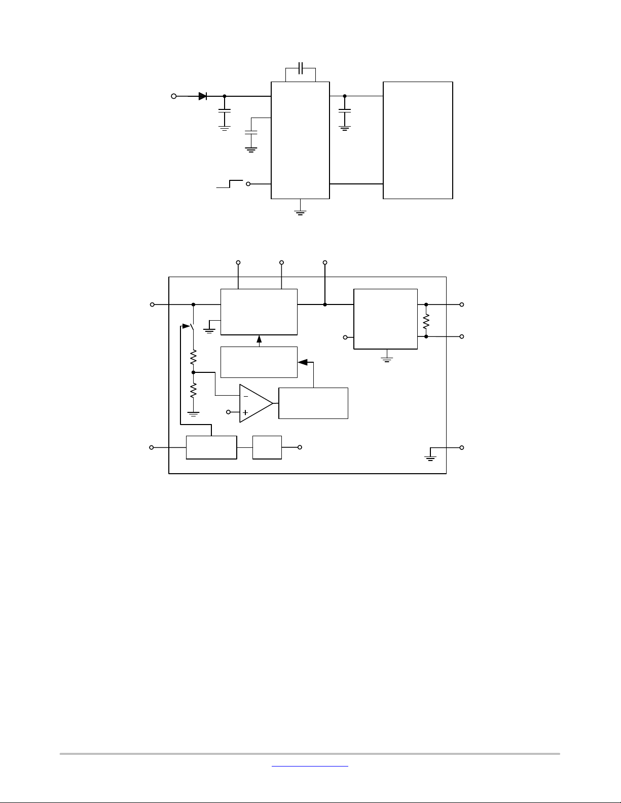
NCV48220
C
FLY
V
BAT
C
in
C+
V
in
V
CP
C
CP
NCV48220
GND
C−
V
out
V
out
C
V
DD
out
Microprocessor
RO
I/OENONOFF
Figure 1. Application Schematic
C+ C− V
V
in
Charge Pump
Power Switches
in1
Charge Pump
Drivers and
R
Logic
CP
LDO
with Overcurrent
and
Overtemperature
Protections
V
ref
and
Reset Circuitry
R
RO
V
RO
out
EN
R
in2
V
Enable
Battery Voltage
ref
V
ref
Monitor
ref
Figure 2. Simplified Block Diagram
GNDV
www.onsemi.com
2
Page 3
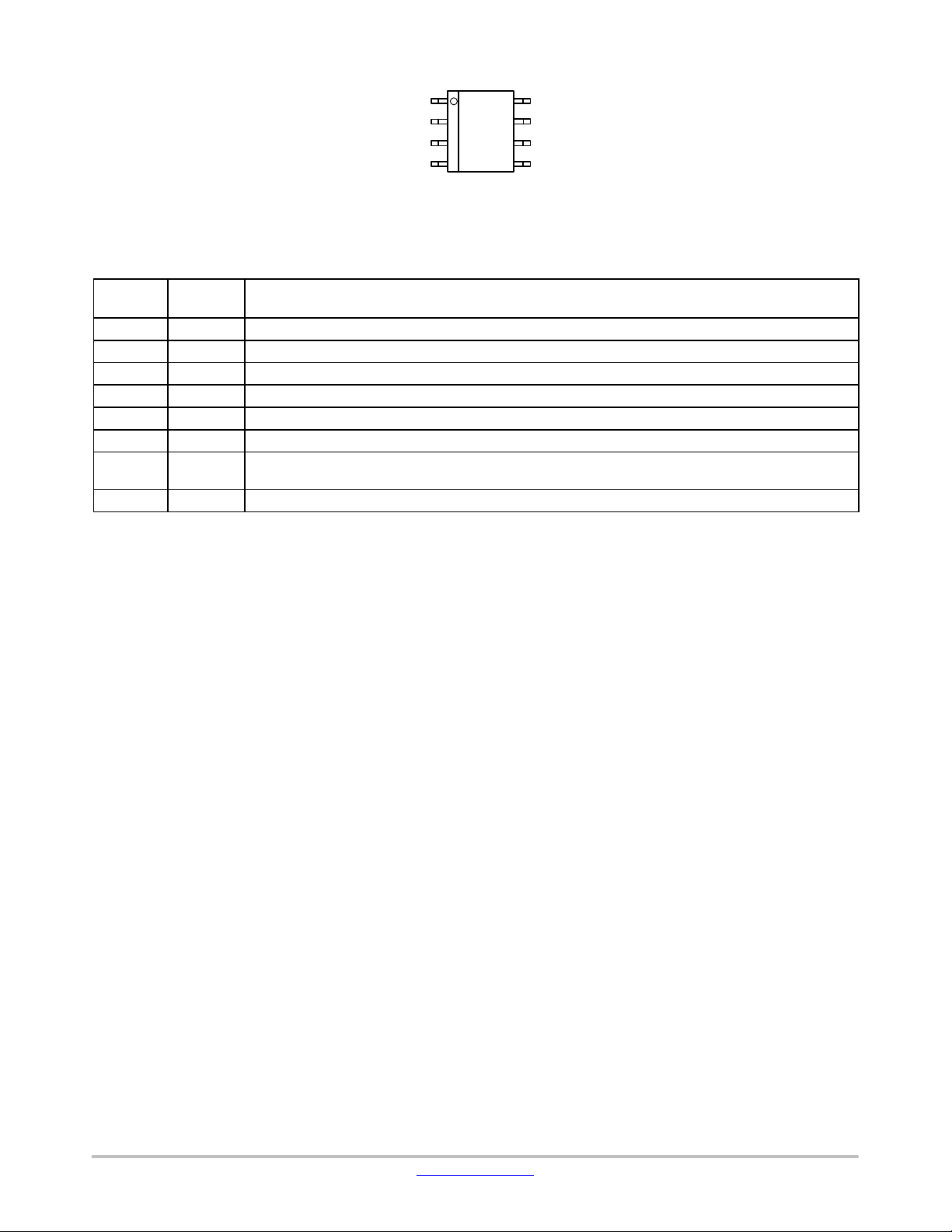
NCV48220
Figure 3. Pin Connections (Top Views)
Table 1. PIN FUNCTION DESCRIPTION
Pin No.
SOIC−8
1 V
2 C+ Flying Capacitor Positive Connection.
3 C− Flying Capacitor Negative Connection.
4 V
5 GND Power Supply Ground.
6 EN Enable Input; low level disables the IC.
7 RO
8 V
Pin Name Description
CP
in
Charge Pump Output Voltage (Input Voltage of LDO).
Charge Pump Input Voltage.
Reset Output. 30 kW internal Pull−up resistor connected between RO and V
out of regulation. See ELECTRICAL CHARACTERISTICS table for delay time specifications.
out
Regulated Output Voltage of LDO.
18
V
CP
C+
C−
V
in
SOIC−8
V
out
RO
EN
GND
. RO goes Low when V
out
out
is
www.onsemi.com
3
Page 4
NCV48220
MAXIMUM RATINGS
Rating Symbol Min Max Unit
Charge Pump Input Voltage DC (Note 1) V
Charge Pump Input Voltage (Note 2)
Load Dump − Suppressed
Charge Pump Output Voltage V
Positive Flying Capacitor Voltage V
Negative Flying Capacitor Voltage V
Regulated Output Voltage V
Enable Input Voltage DC
DC
in
U
S
CP
C+
C−
out
V
EN
Transient, t < 100 ms
Reset Output Voltage V
Maximum Junction Temperature T
Storage Temperature Range T
RO
J(max)
STG
Stresses exceeding those listed in the Maximum Ratings table may damage the device. If any of these limits are exceeded, device functionality
should not be assumed, damage may occur and reliability may be affected.
1. Refer to ELECTRICAL CHARACTERISTICS and APPLICATION INFORMATION for Safe Operating Area.
2. Load Dump Test B (with centralized load dump suppression) according to ISO16750−2 standard. Guaranteed by design. Not tested in
production. Passed Class A according to ISO16750−1.
−0.3 40 V
− 45 V
−0.3 16 V
−0.3 16 V
−0.3 7 V
−0.3 7 V
−0.3
−
40
45
−0.3 7 V
− 150 °C
−55 150 °C
V
ESD CAPABILITY (Note 3)
Rating Symbol Min Max Unit
ESD Capability, Human Body Model ESD
HBM
−2 2 kV
3. This device series incorporates ESD protection and is tested by the following methods:
ESD Human Body Model tested per AEC−Q100−002 (JS−001−2010)
Field Induced Charge Device Model ESD characterization is not performed on plastic molded packages with body sizes <50mm
to the inability of a small package body to acquire and retain enough charge to meet the minimum CDM discharge current waveform
characteristic defined in JEDEC JS−002−2014.
LEAD SOLDERING TEMPERATURE AND MSL (Note 4)
Rating
Moisture Sensitivity Level MSL 1 −
4. For more information, please refer to our Soldering and Mounting Techniques Reference Manual, SOLDERRM/D
Symbol Min Max Unit
THERMAL CHARACTERISTICS
Rating Symbol Value Unit
Thermal Characteristics, SOIC−8
5. Values based on 1s0p board with copper area of 645 mm2 (or 1 in2) of 1 oz copper thickness and FR4 PCB substrate.
6. Values based on 2s2p board with copper area of 645 mm
layers and FR4 PCB substrate.
Thermal Resistance, Junction−to−Air (Note 5)
Thermal Reference, Junction−to−Lead (Note 5)
Thermal Resistance, Junction−to−Air (Note 6)
Thermal Reference, Junction−to−Lead (Note 6)
R
θJA
R
ψJL1
R
θJA
R
ψJL1
2
(or 1 in2) of 1 oz copper thickness for inner layers, 2 oz copper thickness for single
106
62.5
74
59.5
2
°C/W
due
RECOMMENDED OPERATING RANGES
Rating Symbol Min Max Unit
Charge Pump Input Voltage V
LDO Input Voltage V
Junction Temperature T
in
CP
J
3.0 40 V
3.5 14 V
−40 150 °C
Functional operation above the stresses listed in the Recommended Operating Ranges is not implied. Extended exposure to stresses beyond
the Recommended Operating Ranges limits may affect device reliability.
www.onsemi.com
4
Page 5
NCV48220
ELECTRICAL CHARACTERISTICS (V
values T
= 25°C; for min/max values −40°C ≤ TJ ≤ 150°C, unless otherwise noted.) (Note 7)
J
= 13.5 V, VEN = 3 V, ICP = 0 mA, C
in
= 10 mF with ESR ≈ 10 mW, CCP = 10 mF for typical
FLY
Parameter Test Conditions Symbol Min Typ Max Unit
CHARGE PUMP OUTPUT
Undervoltage Lockout
V
Vin rising
falling
V
in
Charge Pump Operating Threshold
Vin rising, Charge Pump deactivated
V
CP_ON_OFF
VCP falling, Charge Pump activated
Charge Pump Voltage Drop (Vin – VCP) Vin = 7 V, I
Charge Pump Output Voltage Limit Vin = 15 V to 40 V
I
= 0.1 mA to 150 mA
out
= 150 mA V
out
V
Charge Pump Output Current Limit VCP = 0 V (shorted to GND) I
Charge Pump Output Impedance Vin = 3 V, I
= 75 mA R
out
Switching Frequency Vin = 3 V f
REGULATOR OUTPUT
Output Voltage (Accuracy %)
Vin = 7 V to 29 V (LDO mode, CP inactive)
I
= 0.1 mA to 150 mA
out
Output Voltage (Accuracy %)
Vin = 3 V (CP active, boosting mode)
I
= 55 mA
out
Output Voltage (Accuracy %) TJ = −40°C to 125°C
V
= 3.3 V (CP active, boosting mode)
in
I
= 120 mA
out
Line Regulation Vin = 7 V to 29 V, I
Load Regulation I
Dropout Voltage (Note 8) I
= 0.1 mA to 150 mA Reg
out
= 150 mA V
out
= 5 mA Reg
out
DISABLE AND QUIESCENT CURRENTS
Disable Current
Quiescent Current, Iq = Iin − I
out
VEN = 0 V,TJ < 85°C I
I
= 0.1 mA, TJ = 25°C
out
I
= 0.1 mA, TJ < 85°C
out
CURRENT LIMIT PROTECTION
V
Current Limit
Short Circuit Current Limit V
= 0.96 x V
out
= 0 V I
out
out_nom
PSRR
Power Supply Ripple Rejection
f = 100 Hz, 0.5 V
p−p
ENABLE
Enable Input Threshold Voltage
V
Logic Low
Logic High
Enable Input Current
Logic High
Logic Low
VEN = 5 V, TJ < 125 °C
VEN = 0 V, TJ < 125 °C
I
I
EN_OFF
RESET OUTPUT
Reset Output Thresholds
High
Low
Reset Output Low Voltage
V
decreasing
out
V
increasing
out
IRO < 200 mA, V
out
> 1 V
V
Integrated Reset Output Pull Up Resistor R
in_UVLO
2.6
2.2
2.8
2.4
3.0
2.6
V
V
6.1
6.3
6.5
5.5
5.7
5.0 5.1
(+2%)
− −
V
W
V
V
DO_CP
CP_LIM
CP_LIM
out_CP
SW
V
out
V
out
5.3
− 320 800 mV
13 14 15
− − 650 mA
− 12 −
400 450 500 kHz
4.9
(−2 %)
4.8
(−4 %)
V
out
4.8
− −
V
(−4 %)
line
load
DO
DIS
I
q
I
LIM
SC
−20 0 20 mV
−40 10 40 mV
− 150 300 mV
− − 1.0
mA
mA
−
35
−
40
−
45
205 − 450 mA
− 320 − mA
PSRR − 60 − dB
th(EN)
2.5
−
−
0.8
−
V
−
mA
−
3
EN_ON
th(RO)
V
ROL
RO
−
90
92.5−95
90.5
− 0.15 0.25 V
15 30 50
5
−
1
% of
V
97
out
kW
www.onsemi.com
5
Page 6
NCV48220
ELECTRICAL CHARACTERISTICS (V
values T
= 25°C; for min/max values −40°C ≤ TJ ≤ 150°C, unless otherwise noted.) (Note 7)
J
= 13.5 V, VEN = 3 V, ICP = 0 mA, C
in
= 10 mF with ESR ≈ 10 mW, CCP = 10 mF for typical
FLY
Parameter UnitMaxTypMinSymbolTest Conditions
RESET OUTPUT
Reset Delay Time (Note 9)
Reset Reaction Time t
Min Available Time
Max Available Time
t
RD
RR
−
102.40128−153.6
16 25 38
ms
ms
THERMAL SHUTDOWN
Thermal Shutdown Temperature (Note 10)
Thermal Shutdown Hysteresis (Note 10) T
T
SD
SH
150 175 195 °C
− 10 − °C
Product parametric performance is indicated in the Electrical Characteristics for the listed test conditions, unless otherwise noted. Product
performance may not be indicated by the Electrical Characteristics if operated under different conditions.
7. Performance guaranteed over the indicated operating temperature range by design and/or characterization tested at T
pulse techniques are used during testing to maintain the junction temperature as close to ambient as possible.
8. Measured when output voltage falls 100 mV below the regulated voltage at V
9. Reset Delay Times can be chosen from list: 0, 2, 4, 8, 16, 32, 64, 128 ms (Reset Delay Time 0 ms represents Power Good function) and
= 13.5 V.
CP
[TJ. Low duty cycle
A
these delay times are factory preset.
10.Values based on design and/or characterization.
www.onsemi.com
6
Page 7

NCV48220
TYPICAL CHARACTERISTICS
70
350
TJ = 25°C
60
300
I
= 100 mA
out
CP inactive
50
40
30
20
, QUIESCENT CURRENT (mA)
10
q
I
0
Vin = 13.5 V
I
= 100 mA
out
1401006020−20
16012080400−40
250
200
150
100
, QUIESCENT CURRENT (mA)
50
q
I
0
20 40
353025151050
TJ, JUNCTION TEMPERATURE (°C) Vin, INPUT VOLTAGE (V)
Figure 4. Quiescent Current vs. Junction
Figure 5. Quiescent Current vs. Input Voltage
Temperature
70
60
50
40
30
5.10
Vin = 13.5 V
5.05
5.00
20
, QUIESCENT CURRENT (mA)
10
q
I
0
6
5
4
3
2
, OUTPUT VOLTAGE (V)
out
1
V
0
Vin = 13.5 V
= 25°C
T
J
120100806040200
I
, OUTPUT CURRENT (mA)
out
Figure 6. Quiescent Current vs. Output
Current
TJ = 25°C
= 75 mA
I
out
Vin increasing at Power Up (from 0 V)
8
Vin, INPUT VOLTAGE (V)
Figure 8. Output Voltage vs. Input Voltage
, OUTPUT VOLTAGE (V)
4.95
out
V
4.90
160140
1401006020−20
16012080400−40
TJ, JUNCTION TEMPERATURE (°C)
Figure 7. Output Voltage vs. Junction
Temperature
300
TJ = 125°C
250
200
150
TJ = 25°C
100
, DROPOUT VOLTAGE (mV)
50
DO
V
0
1412106420
I
, OUTPUT CURRENT (mA)
out
1801501209060300
Figure 9. Dropout Voltage vs. Output Current
www.onsemi.com
7
Page 8

NCV48220
0
TYPICAL CHARACTERISTICS
300
250
200
150
100
, DROPOUT VOLTAGE (mV)
50
DO
V
0
400
350
300
250
200
150
I
= 150 mA
out
1401006020−20
TJ, JUNCTION TEMPERATURE (°C)
Figure 10. Dropout Voltage vs. Junction
Temperature
400
TJ = 25°C
350
300
TJ = 125°C
250
200
150
100
, OUTPUT CURRENT LIMIT (mA)
50
LIM
I
16012080400−40
0
1086420
V
= 0 V
out
161412
Vin, INPUT VOLTAGE (V)
Figure 11. Output Current Limit vs. Input
Voltage
100
Unstable Region
10
Stable Region
1
ESR (W)
100
50
, OUTPUT CURRENT LIMIT (mA)
LIM
I
0
TJ, JUNCTION TEMPERATURE (°C)
Figure 12. Output Current Limit vs. Junction
Temperature
40
30
20
V
10
0
, INPUT VOLTAGE (V)
in
V
−10
in
V
out
−20
1
TIME (ms)
Figure 14. Line Transient
Vin = 13.5 V
V
out
TJ = 25°C
= 5 mA
I
out
t
= 1 ms
rise/fall
C
= 10 mF
out
= 4.8 V
1401006020−20
2.521.50.50−0.5−1
0.1
16012080400−40
7.5
7
6.5
6
5.5
5
4.5
0.01
0 25 50 75 100 125 15
400
350
300
V
250
200
150
, OUTPUT VOLTAGE (V)
100
, OUTPUT CURRENT (mA)
out
V
out
I
50
I
out
0
Vin = 13.5 V
C
= 3.3 mF − 100 mF
out
I
, OUTPUT CURRENT (mA)
out
Figure 13. Output Stability with Output
Capacitor ESR
TJ = 25°C
= 13.5 V
V
in
t
= 1 ms
out
rise/fall
C
out
= 10 mF
0.4
TIME (ms)
Figure 15. Load Transient
5.2
5.1
5.0
4.9
4.8
, OUTPUT VOLTAGE (V)
out
4.7
V
4.6
1
1.20.80.60.20−0.2−0.4
www.onsemi.com
8
Page 9

NCV48220
TYPICAL CHARACTERISTICS
16
V
14
in
12
10
V
8
out
6
4
2
, INPUT VOLTAGE (V)
in
V
0
−2
TJ = 25°C
I
t
C
−4
0.6
TIME (ms)
Figure 16. Power Up Transient Figure 17. PSRR vs. Frequency
10
9
8
TJ = 125°C
7
6
5
4
3
, ENABLE CURRENT (mA)
2
EN
I
1
0
35 9
VEN, ENABLE VOLTAGE (V)
Figure 18. Enable Current vs. Enable Voltage
= 5 mA
out
rise/fall
= 10 mF
out
1.2 1.4
= 1 ms
TJ = 25°C
9
8
7
6
5
4
3
2
1
0
−1
1.610.80.40.20−0.2
PSRR (dB)
, OUTPUT VOLTAGE (V)
out
V
80
70
60
50
40
30
20
10
TJ = 25°C
= 13.5 V
V
in_DC
V
= 0.5 V
I
out
C
in_AC
out
= 150 mA
= 10 mF
p−p
0
10
10M1M100K10K1K100
FREQUENCY (Hz)
45
40
35
TJ = 125°C
30
25
TJ = 25°C
20
15
, ENABLE CURRENT (mA)
10
EN
I
5
0
108764210
V
, ENABLE VOLTAGE (V)
EN
30
4020100
3515525
Figure 19. Enable Current vs. Enable Voltage
10
9
Vin = 13.5 V
8
7
4.8
Vin = 13.5 V
4.75
4.7
6
5
4.65
4
3
, DISABLE CURRENT (mA)
2
dis
I
1
0
20 60 140
16012010080400−20−40
TJ, JUNCTION TEMPERATURE (°C)
Figure 20. Disable Current vs. Junction
Temperature
4.6
4.55
4.5
, OUTPUT VOLTAGE RESET THRESHOLD (V)
rt
V
20 60 140
TJ, JUNCTION TEMPERATURE (°C)
Figure 21. Output Voltage Reset Threshold
vs. Junction Temperature
16012010080400−20−40
www.onsemi.com
9
Page 10

NCV48220
0
TYPICAL CHARACTERISTICS
3.0
2.9
V
2.8
UVLO_Upper
2.7
2.6
V
2.5
THRESHOLD (V)
2.4
, UNDERVOLTAGE LOCKOUT
2.3
UVLO
V
2.2
UVLO_Lower
20 60 140
TJ, JUNCTION TEMPERATURE (°C)
Figure 22. Undervoltage Lockout vs. Junction
Temperature
12
10
8
6
4
IMPEDANCE (W)
, CHARGE PUMP OUTPUT
2
out_CP
R
0
20 60 140
TJ, JUNCTION TEMPERATURE (°C)
Vin = 3 V
= 75 mA
I
out
6.8
6.6
6.4
6.2
6
, CHARGE PUMP
5.8
5.6
CP_ON_OFF
V
OPERATING THRESHOLD (V)
5.4
16012010080400−20−40
5.2
TJ, JUNCTION TEMPERATURE (°C)
Figure 23. Charge Pump Operating Threshold
500
490
480
470
460
450
440
430
420
, SWITCHING FREQUENCY (kHz)
410
SW
F
16012010080400−20−40
400
I
= 100 mA
out
V
CP_OFF
V
CP_ON
20 60 140
vs. Junction Temperature
Vin = 13.5 V
20 60 140
TJ, JUNCTION TEMPERATURE (°C)
12010080400−20−40
16012010080400−20−40
16
Figure 24. Charge Pump Output Impedance
vs. Junction Temperature
15
V
in
V
CP
10
5
, INPUT VOLTAGE (V)
0
in
V
V
out
, CHARGE PUMP OUTPUT VOLTAGE (V)
−5
CP
V
Figure 26. Starting Profile Transient
www.onsemi.com
600
TIME (ms)
10
Figure 25. Switching Frequency vs. Junction
Temperature
6.5
6
TJ = 25°C
= 30 mA
I
out
C
= 4.7 mF
in
C
CP
C
out
1200
= 10 mF
= 10 mF
1400
5.5
, OUTPUT VOLTAGE (V)
5
out
V
4.5
160010008004002000−200
Page 11

V
V
in_UVLO rise
V
in_UVLO fall
V
CP_OFF
V
CP_LIM
V
CP_ON
NCV48220
V
in
t
CP
V
RT + VRH
V
out
V
RT
V
RO
V
ROH
V
ROL
t
RD
Short term
overcurrent
< t
Long term
RR
> t
RR
t
RR
t
RD
t
RR
t
t
t
Figure 27. Reset Function, Charge Pump Function and Timing Diagram
www.onsemi.com
11
Page 12

NCV48220
DEFINITIONS
General
All measurements are performed using short pulse low
duty cycle techniques to maintain junction temperature as
close as possible to ambient temperature.
Output voltage
The output voltage parameter is defined for specific
temperature, input voltage and output current values or
specified over Line, Load and Temperature ranges.
Line Regulation
The change in output voltage for a change in input voltage
measured for specific output current over operating ambient
temperature range.
Load Regulation
The change in output voltage for a change in output
current measured for specific input voltage over operating
ambient temperature range.
Dropout Voltage
The input to output differential at which the regulator
output no longer maintains regulation against further
reductions in input voltage. It is measured when the output
drops 100 mV below its nominal value. The junction
temperature, load current, and minimum input supply
requirements affect the dropout level.
Quiescent and Disable Currents
Quiescent Current (Iq) is the difference between the input
current (measured through the LDO input pin) and the
output load current. If Enable pin is set to LOW the regulator
reduces its internal bias and shuts off the output, this term is
called the disable current (I
DIS
).
Current Limit
Current Limit is value of output current by which output
voltage drops below 96 % of its nominal value.
PSRR
Power Supply Rejection Ratio is defined as ratio of output
voltage and input voltage ripple. It is measured in decibels
(dB).
Line Transient Response
Typical output voltage overshoot and undershoot
response when the input voltage is excited with a given
slope.
Load Transient Response
Typical output voltage overshoot and undershoot
response when the output current is excited with a given
slope between low−load and high−load conditions.
Thermal Protection
Internal thermal shutdown circuitry is provided to protect
the integrated circuit in the event that the maximum junction
temperature is exceeded. When activated at typically 175°C,
the regulator turns off. This feature is provided to prevent
failures from accidental overheating.
Maximum Package Power Dissipation
The power dissipation level is maximum allowed power
dissipation for particular package or power dissipation at
which the junction temperature reaches its maximum
operating value, whichever is lower.
www.onsemi.com
12
Page 13

NCV48220
APPLICATIONS INFORMATION
Circuit Description
The NCV48220 is an integrated low dropout regulator
with integrated battery voltage charge pump boost converter
that provides a regulated voltage at 150 mA to the output.
Device is enabled with an input to the enable pin. The
regulator voltage is provided by a PMOS pass transistor
controlled by an error amplifier with a bandgap reference,
which gives it the lowest possible dropout voltage. The
output current capability is 150 mA, and the base drive
quiescent current is controlled to prevent oversaturation
when the input voltage is low or when the output is
overloaded. Charge pump boost converter is active only
during charge pump output voltage (input voltage of LDO)
decreasing under charge pump operating activation
threshold and inactive after input voltage increasing over
charge pump operating deactivation threshold. Thermal
shutdown occurs above 150°C to protect the IC during
overloads and extreme ambient temperatures.
Regulator
The error amplifier compares the reference voltage to a
sample of the output voltage (V
) and drives the gate of a
out
PMOS series pass transistor via a buffer. The reference is a
bandgap design to give it a temperature−stable output.
Saturation control of the PMOS is a function of the load
current and input voltage. Oversaturation of the output
power device is prevented, and quiescent current in the
ground pin is minimized. Current limit and voltage monitors
complement the regulator design to give safe operating
signals to the processor and control circuits.
Regulator Stability Considerations
The input capacitor (Cin) and charge pump output
capacitor (C
to avoid voltage line influences. The output capacitor (C
) is necessary to stabilize the input impedance
CP
out
helps determine three main characteristics of a linear
regulator: startup delay, load transient response and loop
stability. The capacitor value and type should be based on
cost, availability, size and temperature constraints. The
aluminum electrolytic capacitor is the least expensive
solution, but, if the circuit operates at low temperatures
(−25°C to −40°C), both the value and ESR of the capacitor
will vary considerably. The capacitor manufacturer’s data
sheet usually provides this information. The value for the
output capacitor C
, shown in Figure 1 should work for
out
most applications; see also Figure 13 for output stability at
various load and Output Capacitor ESR conditions. Stable
region of ESR in Figure 13 shows ESR values at which the
LDO output voltage does not have any permanent
oscillations at any dynamic changes of output load current.
Marginal ESR is the value at which the output voltage
waving is fully damped during four periods after the load
change and no oscillation is further observable.
ESR characteristics were measured with ceramic
capacitors and additional series resistors to emulate ESR.
Low duty cycle pulse load current technique has been used
to maintain junction temperature close to ambient
temperature.
List of recommended output capacitors:
GCM31CR71H225MA55 (2.2 mF, 50 V, X7R, 1206)
GCM31CR71C335KA37 (3.3 mF, 16 V, X7R, 1206)
GCM31CR71E475MA55 (4.7 mF, 25 V, X7R, 1206)
GCM31CC71E106MA03 (10 mF, 25 V, X7S, 1206)
KCM55WC71E107MH13 (100 mF, 25 V, X7S, 2220)
CGA5L3X7R1H225M (2.2 mF, 50 V, X7R, 1206)
CGA5L1X7R1E335M (3.3 mF, 25 V, X7R, 1206)
CGA5L1X7R1E475M (4.7 mF, 25 V, X7R, 1206)
CGA5L1X7R1E106M (10 mF, 25 V, X7R, 1206)
CKG57NX7S1C107M (100 mF, 16 V, X7S, 2220)
Charge Pump Capacitor Selection
Low ESR capacitors are necessary to minimize power
losses, especially at high load current during active charge
pump boost mode. The exact value of C
FLY
important. Charge pump output impedance (R
given by equation 1.
R
out_CP
^ 2 S(RSW) )
1
fSW C
) 4 ESR
FLY
Charge pump output voltage ripple is determined by the
value of C
and the load current (I
CP
). CCP is charged and
out
discharged at a current roughly equal to the load current.
I
V
ripple_CP
+
OUT
2 fSW C
CP
This equation doesn’t including the impact of
non−overlap time and C
)
is not being driven during the non−overlap time, this time
capacitor ESR. Since the output
CP
should be included in the ripple calculation. C
discharge time is approximately 60 % of a switching period
V
ripple_CP
+ I
OUT
ǒ
fSW C
) 2 ESR
CP
0.6
For example, with a 450 kHz switching frequency,
a 10 mF C
capacitor with an ESR of 0.25 W and a 100 mA
CP
load the ripple voltage is 65 mV peak to peak.
Enable Input
The enable pin is used to turn the regulator on or off. By
holding the pin below 0.8 V, the output of the regulator will
be turned off. When the voltage on the enable pin is greater
than 2.5 V, the output of the regulator will be enabled to
power its output to the regulated output voltage. The enable
pin may be connected directly to the input pin to give
constant enable to the output regulator.
and CCP is not
) is
out_CP
) ESR
FLY
C
CP
CP
C
(eq. 1)
(eq. 2)
capacitor
(eq. 3)
Ǔ
CP
www.onsemi.com
13
Page 14

NCV48220
Thermal Considerations
As power in the NCV48220 increases, it might become
necessary to provide some thermal relief. The maximum
power dissipation supported by the device is dependent
upon board design and layout. Mounting pad configuration
on the PCB, the board material, and the ambient temperature
affect the rate of junction temperature rise for the part. When
the NCV48220 has good thermal conductivity through the
PCB, the junction temperature will be relatively low with
high power applications. The maximum dissipation the
NCV48220 can handle is given by:
P
D(MAX)
ƪ
T
J(MAX)
+
R
QJA
) T
ƫ
A
(eq. 4)
Since TJ is not recommended to exceed 150°C, then the
2
NCV48220 soldered on 645 mm
, 1 oz copper area, FR4
can dissipate up to 1.2 W and up to 1.7 W for 4 layers PCB
(all layers are 1 oz) when the ambient temperature (T
25 °C. See Figure 28 for R
versus PCB area.
JA
Q
) is
A
Power dissipated is given by three main parts. The first is
dependent on the charge pump boost mode activation. The
second part including the power dissipated on LDO and the
last represent current consumption.
CP active : P
CP inactive : P
P
+ǒV
D_LDO
+ (2 VIN* VCP) I
D_CP1
+ǒVIN* V
D_CP2
CPǒmax. V
CP_LIM
CPǒmax. V
* V
Ǔ
OUT
OUT
CP_LIM
Ǔ
I
(eq. 5)
I
Ǔ
Out
Ǔ
(eq. 6)
(eq. 7)
Out
200
180
160
140
120
2 oz, Single Layer
100
80
, THERMAL RESISTANCE (5C/W)
JA
60
Q
0 200 400 600 800 1000
R
1 oz, Single Layer
1 oz, 4 Layer
Copper heat spreader area (mm2)
Figure 28. Thermal Resistance
vs. PCB Copper Area
Hints
Vin and GND printed circuit board traces should be as
wide as possible. When the impedance of these traces is
high, there is a chance to pick up noise or cause the regulator
to malfunction. Place external components, especially the
output capacitor, as close as possible to the device and make
traces as short as possible.
Place filter components as near as possible to the device to
increase EMC performance.
Input Capacitor C
is required if regulator is located far
in
from power supply filter. If extremely fast input voltage
transients are expected with slew rate in excess of 4 V/ms
then appropriate input filter must be used. The filter can be
composed of several capacitors in parallel.
P
D_Iq
+ Vin ǒI
q@I
OUT
Ǔ
(eq. 8)
The power dissipated by the NCV48220 can be calculated
from the following equations:
PD1+ P
+ P
P
D2
ORDERING INFORMATION
Device Output Voltage Reset Delay Time
NCV48220D50R2G 5.0 V 0 ms V4822050 SOIC−8
†For information on tape and reel specifications, including part orientation and tape sizes, please refer to our Tape and Reel Packaging
Specifications Brochure, BRD8011/D
††For information about another Output Voltage, Reset Delay Time, Packages options contact factory. Reset Delay Time can be chosen from
following list of values: 0, 2, 4, 8, 16, 32, 64 and 128 ms.
D_CP1
D_CP2
) P
) P
D_LDO
D_LDO
) P
) P
D_Iq
D_Iq
(eq. 9)
(eq. 10)
††
Marking Package Shipping
2500 / Tape & Reel
(Pb−Free)
†
www.onsemi.com
14
Page 15

MECHANICAL CASE OUTLINE
PACKAGE DIMENSIONS
8
1
SCALE 1:1
−Y−
−Z−
−X−
A
58
B
1
4
G
H
D
0.25 (0.010) Z
M
SOLDERING FOOTPRINT*
7.0
0.275
S
Y
0.25 (0.010)
C
SXS
SEATING
PLANE
0.10 (0.004)
1.52
0.060
4.0
0.155
CASE 751−07
M
M
Y
N
SOIC−8 NB
ISSUE AK
K
X 45
_
M
J
MARKING DIAGRAM*
8
XXXXX
ALYWX
1
XXXXX = Specific Device Code
A = Assembly Location
L = Wafer Lot
Y = Year
W = Work Week
G = Pb−Free Package
8
XXXXX
ALYWX
G
1
IC
IC
(Pb−Free)
DATE 16 FEB 2011
NOTES:
1. DIMENSIONING AND TOLERANCING PER
ANSI Y14.5M, 1982.
2. CONTROLLING DIMENSION: MILLIMETER.
3. DIMENSION A AND B DO NOT INCLUDE
MOLD PROTRUSION.
4. MAXIMUM MOLD PROTRUSION 0.15 (0.006)
PER SIDE.
5. DIMENSION D DOES NOT INCLUDE DAMBAR
PROTRUSION. ALLOWABLE DAMBAR
PROTRUSION SHALL BE 0.127 (0.005) TOTAL
IN EXCESS OF THE D DIMENSION AT
MAXIMUM MATERIAL CONDITION.
6. 751−01 THRU 751−06 ARE OBSOLETE. NEW
STANDARD IS 751−07.
MILLIMETERS
DIMAMIN MAX MIN MAX
4.80 5.00 0.189 0.197
B 3.80 4.00 0.150 0.157
C 1.35 1.75 0.053 0.069
D 0.33 0.51 0.013 0.020
G 1.27 BSC 0.050 BSC
H 0.10 0.25 0.004 0.010
J 0.19 0.25 0.007 0.010
K 0.40 1.27 0.016 0.050
M 0 8 0 8
____
N 0.25 0.50 0.010 0.020
S 5.80 6.20 0.228 0.244
INCHES
GENERIC
8
XXXXXX
AYWW
1
Discrete
XXXXXX = Specific Device Code
A = Assembly Location
Y = Year
WW = Work Week
G = Pb−Free Package
8
XXXXXX
AYWW
1
Discrete
(Pb−Free)
G
0.6
0.024
1.270
0.050
SCALE 6:1
ǒ
inches
mm
Ǔ
*This information is generic. Please refer to
device data sheet for actual part marking.
Pb−Free indicator, “G” or microdot “G”, may
or may not be present. Some products may
not follow the Generic Marking.
*For additional information on our Pb−Free strategy and soldering
details, please download the ON Semiconductor Soldering and
Mounting Techniques Reference Manual, SOLDERRM/D.
STYLES ON PAGE 2
DOCUMENT NUMBER:
DESCRIPTION:
ON Semiconductor and are trademarks of Semiconductor Components Industries, LLC dba ON Semiconductor or its subsidiaries in the United States and/or other countries.
ON Semiconductor reserves the right to make changes without further notice to any products herein. ON Semiconductor makes no warranty, representation or guarantee regarding
the suitability of its products for any particular purpose, nor does ON Semiconductor assume any liability arising out of the application or use of any product or circuit, and specifically
disclaims any and all liability, including without limitation special, consequential or incidental damages. ON Semiconductor does not convey any license under its patent rights nor the
rights of others.
© Semiconductor Components Industries, LLC, 2019
98ASB42564B
SOIC−8 NB
Electronic versions are uncontrolled except when accessed directly from the Document Repository.
Printed versions are uncontrolled except when stamped “CONTROLLED COPY” in red.
PAGE 1 OF 2
www.onsemi.com
Page 16

STYLE 1:
PIN 1. EMITTER
2. COLLECTOR
3. COLLECTOR
4. EMITTER
5. EMITTER
6. BASE
7. BASE
8. EMITTER
STYLE 5:
PIN 1. DRAIN
2. DRAIN
3. DRAIN
4. DRAIN
5. GATE
6. GATE
7. SOURCE
8. SOURCE
STYLE 9:
PIN 1. EMITTER, COMMON
2. COLLECTOR, DIE #1
3. COLLECTOR, DIE #2
4. EMITTER, COMMON
5. EMITTER, COMMON
6. BASE, DIE #2
7. BASE, DIE #1
8. EMITTER, COMMON
STYLE 13:
PIN 1. N.C.
2. SOURCE
3. SOURCE
4. GATE
5. DRAIN
6. DRAIN
7. DRAIN
8. DRAIN
STYLE 17:
PIN 1. VCC
2. V2OUT
3. V1OUT
4. TXE
5. RXE
6. VEE
7. GND
8. ACC
STYLE 21:
PIN 1. CATHODE 1
2. CATHODE 2
3. CATHODE 3
4. CATHODE 4
5. CATHODE 5
6. COMMON ANODE
7. COMMON ANODE
8. CATHODE 6
STYLE 25:
PIN 1. VIN
2. N/C
3. REXT
4. GND
5. IOUT
6. IOUT
7. IOUT
8. IOUT
STYLE 29:
PIN 1. BASE, DIE #1
2. EMITTER, #1
3. BASE, #2
4. EMITTER, #2
5. COLLECTOR, #2
6. COLLECTOR, #2
7. COLLECTOR, #1
8. COLLECTOR, #1
STYLE 2:
PIN 1. COLLECTOR, DIE, #1
2. COLLECTOR, #1
3. COLLECTOR, #2
4. COLLECTOR, #2
5. BASE, #2
6. EMITTER, #2
7. BASE, #1
8. EMITTER, #1
STYLE 6:
PIN 1. SOURCE
2. DRAIN
3. DRAIN
4. SOURCE
5. SOURCE
6. GATE
7. GATE
8. SOURCE
STYLE 10:
PIN 1. GROUND
2. BIAS 1
3. OUTPUT
4. GROUND
5. GROUND
6. BIAS 2
7. INPUT
8. GROUND
STYLE 14:
PIN 1. N−SOURCE
2. N−GATE
3. P−SOURCE
4. P−GATE
5. P−DRAIN
6. P−DRAIN
7. N−DRAIN
8. N−DRAIN
STYLE 18:
PIN 1. ANODE
2. ANODE
3. SOURCE
4. GATE
5. DRAIN
6. DRAIN
7. CATHODE
8. CATHODE
STYLE 22:
PIN 1. I/O LINE 1
2. COMMON CATHODE/VCC
3. COMMON CATHODE/VCC
4. I/O LINE 3
5. COMMON ANODE/GND
6. I/O LINE 4
7. I/O LINE 5
8. COMMON ANODE/GND
STYLE 26:
PIN 1. GND
2. dv/dt
3. ENABLE
4. ILIMIT
5. SOURCE
6. SOURCE
7. SOURCE
8. VCC
STYLE 30:
PIN 1. DRAIN 1
2. DRAIN 1
3. GATE 2
4. SOURCE 2
5. SOURCE 1/DRAIN 2
6. SOURCE 1/DRAIN 2
7. SOURCE 1/DRAIN 2
8. GATE 1
SOIC−8 NB
CASE 751−07
ISSUE AK
STYLE 3:
STYLE 7:
STYLE 11:
STYLE 15:
STYLE 19:
STYLE 23:
PIN 1. DRAIN, DIE #1
2. DRAIN, #1
3. DRAIN, #2
4. DRAIN, #2
5. GATE, #2
6. SOURCE, #2
7. GATE, #1
8. SOURCE, #1
PIN 1. INPUT
2. EXTERNAL BYPASS
3. THIRD STAGE SOURCE
4. GROUND
5. DRAIN
6. GATE 3
7. SECOND STAGE Vd
8. FIRST STAGE Vd
PIN 1. SOURCE 1
2. GATE 1
3. SOURCE 2
4. GATE 2
5. DRAIN 2
6. DRAIN 2
7. DRAIN 1
8. DRAIN 1
PIN 1. ANODE 1
2. ANODE 1
3. ANODE 1
4. ANODE 1
5. CATHODE, COMMON
6. CATHODE, COMMON
7. CATHODE, COMMON
8. CATHODE, COMMON
PIN 1. SOURCE 1
2. GATE 1
3. SOURCE 2
4. GATE 2
5. DRAIN 2
6. MIRROR 2
7. DRAIN 1
8. MIRROR 1
PIN 1. LINE 1 IN
2. COMMON ANODE/GND
3. COMMON ANODE/GND
4. LINE 2 IN
5. LINE 2 OUT
6. COMMON ANODE/GND
7. COMMON ANODE/GND
8. LINE 1 OUT
STYLE 27:
PIN 1. ILIMIT
2. OVLO
3. UVLO
4. INPUT+
5. SOURCE
6. SOURCE
7. SOURCE
8. DRAIN
DATE 16 FEB 2011
STYLE 4:
PIN 1. ANODE
2. ANODE
3. ANODE
4. ANODE
5. ANODE
6. ANODE
7. ANODE
8. COMMON CATHODE
STYLE 8:
PIN 1. COLLECTOR, DIE #1
2. BASE, #1
3. BASE, #2
4. COLLECTOR, #2
5. COLLECTOR, #2
6. EMITTER, #2
7. EMITTER, #1
8. COLLECTOR, #1
STYLE 12:
PIN 1. SOURCE
2. SOURCE
3. SOURCE
4. GATE
5. DRAIN
6. DRAIN
7. DRAIN
8. DRAIN
STYLE 16:
PIN 1. EMITTER, DIE #1
2. BASE, DIE #1
3. EMITTER, DIE #2
4. BASE, DIE #2
5. COLLECTOR, DIE #2
6. COLLECTOR, DIE #2
7. COLLECTOR, DIE #1
8. COLLECTOR, DIE #1
STYLE 20:
PIN 1. SOURCE (N)
2. GATE (N)
3. SOURCE (P)
4. GATE (P)
5. DRAIN
6. DRAIN
7. DRAIN
8. DRAIN
STYLE 24:
PIN 1. BASE
2. EMITTER
3. COLLECTOR/ANODE
4. COLLECTOR/ANODE
5. CATHODE
6. CATHODE
7. COLLECTOR/ANODE
8. COLLECTOR/ANODE
STYLE 28:
PIN 1. SW_TO_GND
2. DASIC_OFF
3. DASIC_SW_DET
4. GND
5. V_MON
6. VBULK
7. VBULK
8. VIN
DOCUMENT NUMBER:
DESCRIPTION:
ON Semiconductor and are trademarks of Semiconductor Components Industries, LLC dba ON Semiconductor or its subsidiaries in the United States and/or other countries.
ON Semiconductor reserves the right to make changes without further notice to any products herein. ON Semiconductor makes no warranty, representation or guarantee regarding
the suitability of its products for any particular purpose, nor does ON Semiconductor assume any liability arising out of the application or use of any product or circuit, and specifically
disclaims any and all liability, including without limitation special, consequential or incidental damages. ON Semiconductor does not convey any license under its patent rights nor the
rights of others.
© Semiconductor Components Industries, LLC, 2019
98ASB42564B
SOIC−8 NB
Electronic versions are uncontrolled except when accessed directly from the Document Repository.
Printed versions are uncontrolled except when stamped “CONTROLLED COPY” in red.
PAGE 2 OF 2
www.onsemi.com
Page 17

ON Semiconductor and are trademarks of Semiconductor Components Industries, LLC dba ON Semiconductor or its subsidiaries in the United States and/or other countries.
ON Semiconductor owns the rights to a number of patents, trademarks, copyrights, trade secrets, and other intellectual property. A listing of ON Semiconductor’s product/patent
coverage may be accessed at www.onsemi.com/site/pdf/Patent−Marking.pdf
ON Semiconductor makes no warranty, representation or guarantee regarding the suitability of its products for any particular purpose, nor does ON Semiconductor assume any liability
arising out of the application or use of any product or circuit, and specifically disclaims any and all liability, including without limitation special, consequential or incidental damages.
Buyer is responsible for its products and applications using ON Semiconductor products, including compliance with all laws, regulations and safety requirements or standards,
regardless of any support or applications information provided by ON Semiconductor. “Typical” parameters which may be provided in ON Semiconductor data sheets and/or
specifications can and do vary in different applications and actual performance may vary over time. All operating parameters, including “Typicals” must be validated for each customer
application by customer’s technical experts. ON Semiconductor does not convey any license under its patent rights nor the rights of others. ON Semiconductor products are not
designed, intended, or authorized for use as a critical component in life support systems or any FDA Class 3 medical devices or medical devices with a same or similar classification
in a foreign jurisdiction or any devices intended for implantation in the human body. Should Buyer purchase or use ON Semiconductor products for any such unintended or unauthorized
application, Buyer shall indemnify and hold ON Semiconductor and its officers, employees, subsidiaries, affiliates, and distributors harmless against all claims, costs, damages, and
expenses, and reasonable attorney fees arising out of, directly or indirectly, any claim of personal injury or death associated with such unintended or unauthorized use, even if such
claim alleges that ON Semiconductor was negligent regarding the design or manufacture of the part. ON Semiconductor is an Equal Opportunity/Affirmative Action Employer. This
literature is subject to all applicable copyright laws and is not for resale in any manner.
. ON Semiconductor reserves the right to make changes without further notice to any products herein.
PUBLICATION ORDERING INFORMATION
LITERATURE FULFILLMENT:
Email Requests to: orderlit@onsemi.com
ON Semiconductor Website: www.onsemi.com
TECHNICAL SUPPORT
North American Technical Support:
Voice Mail: 1 800−282−9855 Toll Free USA/Canada
Phone: 011 421 33 790 2910
Europe, Middle East and Africa Technical Support:
Phone: 00421 33 790 2910
For additional information, please contact your local Sales Representative
◊
www.onsemi.com
1
 Loading...