

Page 1
NCV47411
LDO Regulator - Adjustable
Dual, Adjustable Current
Limit
3.3 V to 20 V
The NCV47411 is a dual integrated low dropout regulator with
100 mA per channel designed for use in harsh automotive
environments. It includes wide operating temperature and input
voltage ranges. The device is offered with adjustable voltage version
available in 3% output voltage accuracy. It has a high peak input
voltage tolerance and reverse input voltage protection. It also provides
overcurrent protection, overtemperature protection and enable for
control of the state of the output voltage of each channel. The
integrated current sense feature provides diagnosis and system
protection functionality. The current limit of the device is adjustable
by resistor connected to CSO pin for each channel. CSO pin output
current creates voltage drop across CSO resistor which is proportional
to output current of each channel.
Features
• Two Adjustable Outputs: (from 3.3 V to 20 V) ±3% Output Voltage
• Enable Inputs (3.3 V Logic Compatible Thresholds)
• Adjustable Current Limit up to 150 mA
• Protection Features:
♦ Current Limitation
♦ Thermal Shutdown
♦ Reverse Input Voltage
• This is a Pb−Free Device
Typical Applications
• Audio and Infotainment System
• Instrument Cluster
• Navigation
• Satellite Radio
http://onsemi.com
MARKING
DIAGRAM
14
14
1
NCV47411 = Specific Device Code
A = Assembly Location
L = Wafer Lot
Y = Year
W = Work Week
G = Pb−Free Package
(Note: Microdot may be in either location)
V
in
CSO1
EN1
GND
EN2
CSO2
V
in
See detailed ordering and shipping information on page 12 of
this data sheet.
TSSOP−14 EP
CASE 948AW
PIN CONNECTIONS
Top View
114
EPAD
ORDERING INFORMATION
NCV4
7411
ALYWG
G
1
V
out1
ADJ1
NC
NC
NC
ADJ2
V
out2
© Semiconductor Components Industries, LLC, 2013
September, 2019 − Rev. 1
1 Publication Order Number:
NCV47411/D
Page 2
NCV47411
C
1 mF
**
V
in
in
EN1
NCV47411
EN2
GND
V
out1
ADJ1
CSO1
V
out2
ADJ2
CSO2
C
C
CSO1
1 mF
CSO2
1 mF
C
*
b1
R
C
*
b2
R
CSO1
CSO2
R
11
C
R
12
R
21
R
22
out1
10 mF
C
out2
10 mF
Cb1*, Cb2* − Optional, see Regulator Stability Considerations section
** − Both V
pins must be connected together on PCB
in
Figure 1. Application Schematic
(See Application Section for More Datails)
V
in
V
out1
EN1
GND
V
EN2
V
VOLTAGE
REFERENCE
V
REF 1
REF 2
PASS DEVICE 1
I
CSO1
= I
/ 50
out1
AND
ENABLE
SATURATION
PROTECTION
THERMAL
SHUTDOWN
SP1
TSD1
CURRENT MIRROR
SP1
+
−
V
REF 1
1.275 V
V
REF 2
+
2.55 V
−
CSO1
ADJ1
TSD1
in
I
= I
PASS DEVICE 2
CSO2
out2
/ 50
V
out2
AND
ENABLE
SATURATION
PROTECTION
THERMAL
SHUTDOWN
SP2
TSD2
CURRENT MIRROR
+
−
V
REF 2
2.55 V
CSO2
SP2
V
REF 1
+
1.275 V
−
ADJ2
TSD2
Figure 2. Simplified Block Diagram
http://onsemi.com
2
Page 3
NCV47411
Table 1. PIN FUNCTION DESCRIPTION
Pin No. Pin Name Description
1 V
2 CSO1 Current Sense Output 1, Current Limit setting and Output Current value information. See Application
3 EN1 Enable Input 1; low level disables the Channel 1.
4 GND Power Supply Ground.
5 EN2 Enable Input 2; low level disables the Channel 2.
6 CSO2 Current Sense Output 2, Current Limit setting and Output Current value information. See Application
7 V
8 V
9 ADJ2 Adjustable Voltage Setting Input 2. See Application Section for more details.
10 NC Not Connected. (Not internally bonded)
11 NC Not Connected. (Not internally bonded)
12 NC Not Connected. (Not internally bonded)
13 ADJ1 Adjustable Voltage Setting Input 1. See Application Section for more details.
14 V
EPAD EPAD Exposed Pad is connected to Ground. Connect to GND plane on PCB.
in
in
out2
out1
Power Supply Input. (All Vin pins must be connected on PCB)
Section for more details.
Section for more details.
Power Supply Input. (All Vin pins must be connected on PCB)
Regulated Output Voltage 2.
Regulated Output Voltage 1.
http://onsemi.com
3
Page 4
NCV47411
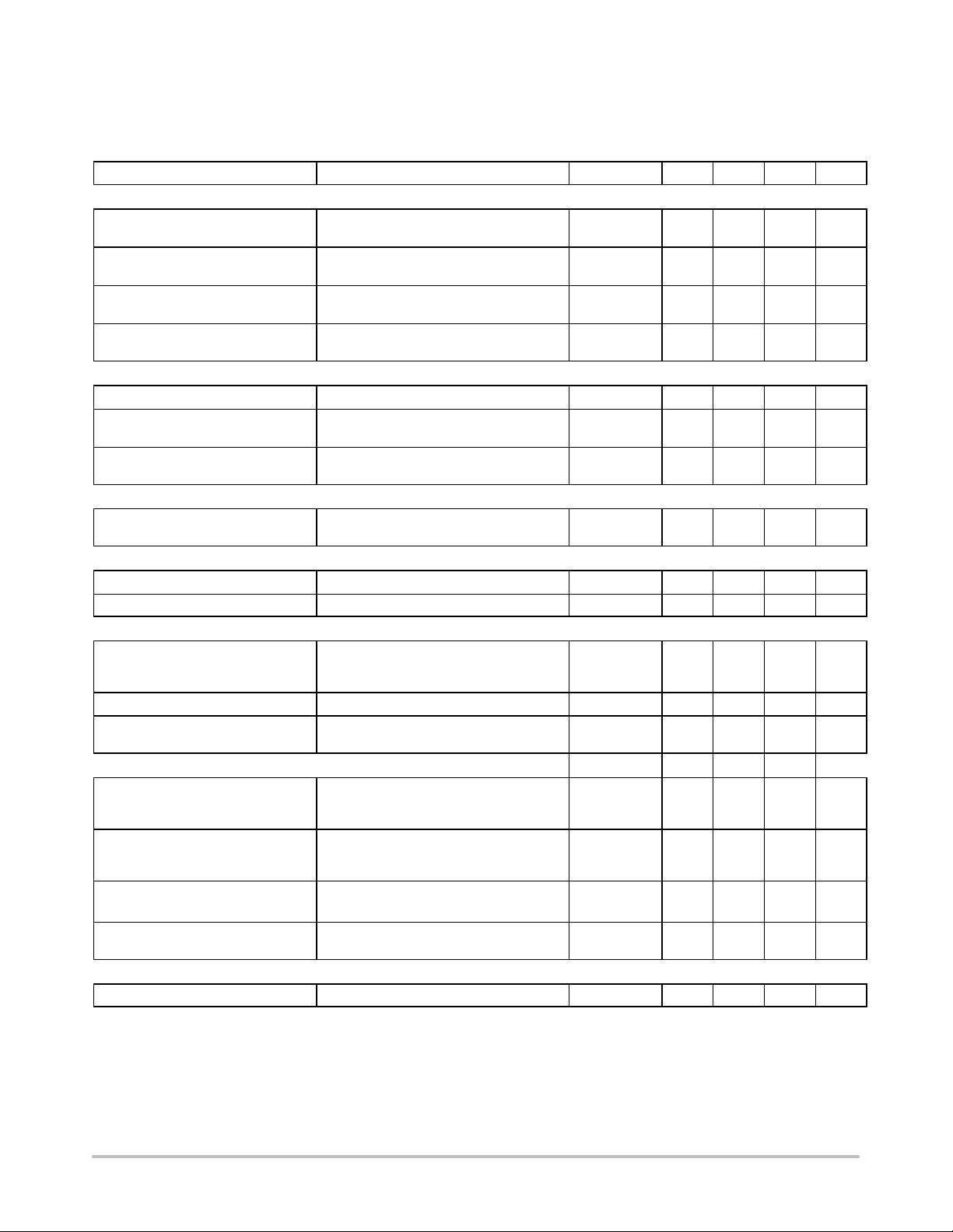
Table 2. ABSOLUTE MAXIMUM RATINGS
Rating Symbol Min Max Unit
Input Voltage DC V
Enable Input Voltage V
ADJ Input Voltage V
CSO Voltage V
Output Voltage V
Junction Temperature T
Storage Temperature T
in
EN1,2
ADJ1,2
CSO1,2
out1,2
J
STG
Stresses exceeding those listed in the Maximum Ratings table may damage the device. If any of these limits are exceeded, device functionality
should not be assumed, damage may occur and reliability may be affected.
Table 3. ESD CAPABILITY (Note 1)
Rating
ESD Capability, Human Body Model ESD
ESD Capability, Machine Model ESD
1. This device series incorporates ESD protection and is tested by the following methods:
a) ESD Human Body Model tested per AEC−Q100−002 (JS−001−2010)
b) ESD Machine Model tested per AEC−Q100−003 (EIA/JESD22−A115)
Symbol Min Max Unit
HBM
MM
−42 45 V
−42 45 V
−0.3 10 V
−0.3 7 V
−1 40 V
−40 150 °C
−55 150 °C
−2 2 kV
−200 200 V
Table 4. LEAD SOLDERING TEMPERATURE AND MSL (Note 2)
Rating Symbol Min Max Unit
Moisture Sensitivity Level MSL 1 1 −
Lead Temperature Soldering
Reflow (SMD Styles Only), Pb−Free Versions
T
SLD
− 265 peak
°C
2. For more information, please refer to our Soldering and Mounting Techniques Reference Manual, SOLDERRM/D
Table 5. THERMAL CHARACTERISTICS (Note 3)
Rating Symbol Value Unit
Thermal Characteristics (single layer PCB)
Thermal Resistance, Junction−to−Air (Note 4)
Thermal Reference, Junction−to−Lead (Note 4)
R
θJA
R
ψJL
52
9.5
Thermal Characteristics (4 layers PCB)
Thermal Resistance, Junction−to−Air (Note 4)
Thermal Reference, Junction−to−Lead (Note 4)
3. Refer to ELECTRICAL CHARACTERISTIS and APPLICATION INFORMATION for Safe Operating Area.
4. Values based on copper area of 645 mm
2
(or 1 in2) of 1 oz copper thickness and FR4 PCB substrate, assuming equal power dissipation
R
θJA
R
ψJL
28.5
8.4
°C/W
°C/W
of both channels. Single layer − according to JEDEC51.3, 4 layers − according to JEDEC51.7
Table 6. RECOMMENDED OPERATING RANGES
Rating Symbol Min Max Unit
Input Voltage (Note 5) V
Nominal Output Voltages V
Output Current Limit (Note 6) I
Junction Temperature T
Current Sense Output (CSO) Capacitor C
in
out_nom1,2
LIM1,2
J
CSO1,2
Functional operation above the stresses listed in the Recommended Operating Ranges is not implied. Extended exposure to stresses beyond
the Recommended Operating Ranges limits may affect device reliability.
5. Minimum V
6. Corresponding R
= 4.4 V or (V
in
out_nom1,2
is in range from 12.75 kW down to 850 W.
CSO1,2
+ 0.5 V), whichever is higher.
4.4 40 V
3.3 20 V
10 150 mA
−40 150 °C
1.0 4.7
mF
http://onsemi.com
4
Page 5
NCV47411
Table 7. ELECTRICAL CHARACTERISTICS
Vin = 13.5 V, V
temperature range −40°C ≤ T
values are referenced to T
REGULATOR OUTPUTS
Output Voltage (Accuracy %)
(Note 8)
Line Regulation
(Note 8)
Load Regulation Vin = (V
Dropout Voltage
(Note 9)
DISABLE AND QUIESCENT CURRENTS
Disable Current
Quiescent Current,
I
= Iin − (I
q
out1
Quiescent Current,
I
= Iin − (I
q
out1
CURRENT LIMIT PROTECTION
Current Limit
PSRR & NOISE
Power Supply Ripple Rejection
Output Noise Voltage f = 10 Hz to 100 kHz, C
ENABLE
Enable Input Threshold Voltage
Logic Low (OFF)
Logic High (ON)
Enable Input Current V
Turn On Time
from Enable ON to 90% of V
OUTPUT CURRENT SENSE
CSO Voltage Level at Current Limit V
CSO Transient Voltage Level
Output Current to CSO Current Ratio
(Note 10)
CSO Current at no Load Current
THERMAL SHUTDOWN
Thermal Shutdown Temperature
Product parametric performance is indicated in the Electrical Characteristics for the listed test conditions, unless otherwise noted. Product
performance may not be indicated by the Electrical Characteristics if operated under different conditions.
7. Performance guaranteed over the indicated operating temperature range by design and/or characterization tested at T
pulse techniques are used during testing to maintain the junction temperature as close to ambient as possible.
8. Minimum input voltage V
9. Measured when the output voltage V
10.Not guaranteed in dropout.
= 3.3 V, R
EN1,2
Parameter
+ I
)
out2
+ I
)
out2
= 0 W, C
CSO1,2
≤ +150°C unless noted otherwise and are guaranteed by test, design or statistical correlation. Typical
J
=25°C (Note 7)
J
= 1 mF, Cin = 1 mF, C
CSO1,2
= 10 mF, ESR = 1.5 W. Min and Max values are valid for
out1,2
Test Conditions Symbol Min Typ Max Unit
out
is 4.4 V or (V
in_min
Vin = V
I
out1,2
Vin = V
I
out1,2
I
out1,2
V
out_nom1,2
V
DO1,2
V
EN1,2
I
out1,2
V
= (V
in
I
out1,2
V
= (V
in
V
out1,2
Vin = (V
f = 100 Hz, 0.5 V
V
out1,2
V
out1,2
EN1,2
I
out1,2
= 82 kW, Rn2 = 27 kW
R
n1
out1,2
(V
out_nom1,2
R
CSO1,2
C
CSO1,2
I
out1,2
tr = 1 ms
V
CSO1,2
(V
out_nom1,2
V
CSO1,2
(V
out_nom1,2
I
out1,2
has dropped by 2% of V
out1,2
to 40 V
in_min
= 5 mA to 100 mA
to (V
in_min
= 5 mA
out_nom1,2
= 5 mA to 100 mA
= Vin − V
= 5 V, I
out1,2
out_nom1,2
+ 8.5 V)
out1,2
+ 20 V)
Reg
= 100 mA
= 0 V I
= 500 mA,
out_nom1,2
+ 8.5 V)
= 100 mA,
out_nom1,2
=
0.9 x V
out_nom1,2
+ 8.5 V)
out_nom1,2
+ 8.5 V)
p−p1,2
= 10 nF V
b1,2
≤ 0.1 V
≥ 0.9 x V
out_nom1,2
= 3.3 V I
= 100 mA, C
= 0.9 x V
= 5 V)
= 10 nF,
b1,2
out_nom1,2
,
V
= 2.55 kW
= 4.7 mF, R
pulse from 10 mA to 100 mA,
= 2 V, I
out1,2
= 5 V)
= 0 V, I
out1,2
= 5 V)
= 2.55 kW
CSO1,2
= 10 mA to 100 mA
= 0 mA,
I
out1,2/ICSO1,2
I
= 2.5 mA T
out_nom1,2
+ 1 V) whichever is higher
from the nominal value obtained at Vin=V
out1,2
V
out1,2
Reg
line1,2
load1,2
V
DO1,2
DIS
I
q
I
q
I
LIM1,2
PSRR
1,2
n1,2
V
th(EN1,2)
EN1,2
t
on
CSO_Ilim1.2
V
CSO1,2
CSO_off1,2
SD1,2
−3 − +3 %
− 0.05 1.0 %
− 0.05 1.4 %
− 250 550 mV
− 0.07 10
− 235 370
− 15 50 mA
150 − − mA
− 75 − dB
− 130 −
0.99−1.8
1.9−2.31
2 9 20
− 1.6 −
2.346
2.55 2.754
(−8 %)
− − 3.3 V
−
50 −
(−10 %)
− − 10
150 − 195 °C
≈ TJ. Low duty cycle
A
out_nom1,2
(+8 %)
(+10 %)
+ 8.5 V.
mV
mA
mA
rms
V
mA
ms
V
−
mA
http://onsemi.com
5
Page 6

NCV47411
TYPICAL CHARACTERISTICS
1.3
1.29
1.28
Vin = 13.5 V
= 5 mA
I
out1,2
400
350
300
250
1.27
200
1.26
1.25
, REFERENCE VOLTAGE (V)
1.24
REF1
V
1.23
−40 −20 0 20 40 60 80 100 160120 140
TJ, JUNCTION TEMPERATURE (°C)
150
100
, QUIESCENT CURRENT (mA)
50
q
I
0
0 5 10 15 20 25 4030 35
Vin, INPUT VOLTAGE (V)
TJ = 25°C
I
out1,2
V
out_nom1,2
Figure 3. Reference Voltage vs. Temperature Figure 4. Quiescent Current vs. Input Voltage
1.4
TJ = 25°C
1.2
I
out1,2
= 5 mA
1
0.8
0.6
0.4
, REFERENCE VOLTAGE (V)
0.2
REF1
V
0
0.5 1.5 2.5 3.5 4.5
01234 5
, INPUT VOLTAGE (V)
V
in
0
TJ = 25°C
−1
R
= 4.7 kW
out1,2
−2
V
out_nom1,2
= 5 V
−3
−4
−5
−6
, INPUT CURRENT (mA)
in
I
−7
−8
−45
−40 −35 −30 −25 −20 −5−15 −10 0
V
, INPUT VOLTAGE (V)
in
Figure 5. Reference Voltage vs. Input Voltage Figure 6. Input Current vs. Input Voltage
(Reverse Input Voltage)
= 500 mA
= 5 V
45
500
Vin = 13.5 V
450
400
V
out_nom1,2
= 5 V
TJ = 150°C
350
300
TJ = 25°C
250
200
150
, DROPOUT VOLTAGE (mV)
100
DO1,2
50
V
TJ = −40°C
0
0 20 40 60 100 120 140 160
I
, OUTPUT CURRENT (mA)
out1,2
80
490
V
= 4.5 V
out1,2
470
450
V
out_nom1,2
= 5 V
430
410
390
(mA)
370
350
330
, OUTPUT CURRENT LIMIT
310
LIM1,2
I
290
270
0 5 10 15 20 25 30 35
V
TJ = −40°C
TJ = 25°C
TJ = 150°C
, INPUT VOLTAGE (V)
in
Figure 7. Dropout Voltage vs. Output Current Figure 8. Output Current Limit vs. Input
Voltage
http://onsemi.com
6
40 45
Page 7

NCV47411
TYPICAL CHARACTERISTICS
160
V
= 3.3 V to 20 V
140
out1,2
= 25°C
T
J
120
100
80
60
40
, OUTPUT CURRENT LIMIT (mA)
20
LIM1,2
0
I
04812
261014
R
, (kW)
CSO1,2
Figure 9. Output Current Limit vs. R
CSO
3.0
TJ = 25°C
2.5
V
in
= V
out_nom1,2
+ 8.5 V
2.0
3.0
V
= 3.3 V to 20 V
out1,2
= 25°C
T
J
2.5
I
= 10 mA to 150 mA
LIM1,2
2.0
1.5
, CSO VOLTAGE (V)
1.0
CSO1,2
0.5
V
0
0 25 50 75 100 125
, OUTPUT CURRENT (% of I
I
out1,2
Figure 10. Output Current (% of I
LIM
Voltage
16
TJ = 25°C
14
12
10
V
in
= V
out_nom1,2
+ 8.5 V
)
LIM1,2
) vs. CSO
1.5
1.0
0.5
, QUIESCENT CURRENT (mA)
q
I
0
0510
, OUTPUT CURRENT (mA)
I
out1,2
Figure 11. Quiescent Current vs. Output Current
(Low Load)
51.0
TJ = 25°C
50.8
50.6
V
in
= V
out_nom1,2
+ 8.5 V
50.4
50.2
50.0
49.8
, OUTPUT CURRENT TO
49.6
CSO1,2
49.4
CSO CURRENT RATIO (−)
/I
49.2
out1,2
I
49.0
0 1 10 100
I
, OUTPUT CURRENT (mA)
out1,2
Figure 13. Output Current to CSO Current
Ratio vs. Output Current
15
8
6
4
, QUIESCENT CURRENT (mA)
2
q
I
0
20
0 10 20 90 10030 80706040 50
Figure 12. Quiescent Current vs. Output Current
50.0
48.0
46.0
44.0
42.0
40.0
38.0
, OUTPUT CURRENT TO
36.0
CSO1,2
34.0
CSO CURRENT RATIO (−)
/I
32.0
out1,2
I
30.0
1000
0 1 10 100 1000
Figure 14. Output Current to CSO Current
Ratio vs. Output Current (In Dropout)
I
, OUTPUT CURRENT (mA)
out1,2
(High Load)
TJ = 25°C
V
in
V
out_nom1,2
, OUTPUT CURRENT (mA)
I
out1,2
= 4.5 V
= 5 V
http://onsemi.com
7
Page 8

NCV47411
TYPICAL CHARACTERISTICS
100
Unstable Region
Area above curves
V
out_nom1,2
10
V
1
out_nom1,2
= 5 V
V
out_nom1,2
= 3.3 V
ESR (W)
0.1
Stable Region
Area below curves
0.01
0 40 120
20 60
I
, OUTPUT CURRENT (mA)
out1,2
TJ = 25°C
= V
V
in
out_nom1,2
C
= 10−100 mF,
out1,2
C
= none
b1,2
Figure 15. Output Capacitor Stability Region
vs. Output Current
100
I
out1,2
= 5 mA
90
80
70
(dB)
1,2
60
I
= 100 mA
out1,2
50
PSRR
40
TJ = 25°C
= 13.5 V (DC) + 0.5 VPP (AC)
V
in
30
V
out_nom1,2
20
10 100 1000 10000 100000
= 5 V
Figure 17. PSRR vs. Frequency
= 20 V
+ 8.5 V
10080
FREQUENCY (Hz)
1400
1200
1000
)
1/2
800
600
(nV/HZ
TJ = 25°C
400
, OUTPUT NOISE DENSITY
n1,2
200
V
= 12 V
V
in
C
= 10 nF
b1,2
I
= 5 mA
out1,2
0
10 100 1000 10000 100000
f = 10 Hz − 100 kHz
V
= 125 mV
n1,2
rms
FREQUENCY (Hz)
Figure 16. Noise vs. Frequency
http://onsemi.com
8
Page 9

NCV47411
DEFINITIONS
General
All measurements are performed using short pulse low
duty cycle techniques to maintain junction temperature as
close as possible to ambient temperature.
Output voltage
The output voltage parameter is defined for specific
temperature, input voltage and output current values or
specified over Line, Load and Temperature ranges.
Line Regulation
The change in output voltage for a change in input voltage
measured for specific output current over operating ambient
temperature range.
Load Regulation
The change in output voltage for a change in output
current measured for specific input voltage over operating
ambient temperature range.
Dropout Voltage
The input to output differential at which the regulator
output no longer maintains regulation against further
reductions in input voltage. It is measured when the output
drops 2% of V
out_nom_n
below its nominal value. The
junction temperature, load current, and minimum input
supply requirements affect the dropout level.
Quiescent and Disable Currents
Quiescent Current (Iq) is the difference between the input
current (measured through the LDO input pin) and the
output load current. If Enable pin is set to LOW the regulator
reduces its internal bias and shuts off the output, this term is
called the disable current (I
DIS
).
Current Limit
Current Limit is value of output current by which output
voltage drops below 90% of its nominal value.
PSRR
Power Supply Rejection Ratio is defined as ratio of output
voltage and input voltage ripple. It is measured in decibels
(dB).
Line Transient Response
Typical output voltage overshoot and undershoot
response when the input voltage is excited with a given
slope.
Load Transient Response
Typical output voltage overshoot and undershoot
response when the output current is excited with a given
slope between low-load and high-load conditions.
Thermal Protection
Internal thermal shutdown circuitry is provided to protect
the integrated circuit in the event that the maximum junction
temperature is exceeded. When activated at typically 175°C,
the regulator turns off. This feature is provided to prevent
failures from accidental overheating.
Maximum Package Power Dissipation
The power dissipation level is maximum allowed power
dissipation for particular package or power dissipation at
which the junction temperature reaches its maximum
operating value, whichever is lower.
http://onsemi.com
9
Page 10

NCV47411
APPLICATIONS INFORMATION
Circuit Description
The NCV47411 is an integrated dual low dropout
regulator that provides a regulated voltage at 100 mA to
each output. It is enabled with an input to the enable pin. The
regulator voltage is provided by a PNP pass transistor
controlled by an error amplifier with a bandgap reference,
which gives it the lowest possible dropout voltage. The
output current capability is 100 mA per output, and the base
drive quiescent current is controlled to prevent
oversaturation when the input voltage is low or when the
output is overloaded. The integrated current sense feature
provides diagnosis and system protection functionality. The
current limit of the device is adjustable by resistor connected
to CSO1,2 pin. Voltage on CSO1,2 pin is proportional to
output current. The regulator is protected by both current
limit and thermal shutdown. Thermal shutdown occurs
above 150°C to protect the IC during overloads and extreme
ambient temperatures.
Regulator
The error amplifier compares the reference voltage to a
sample of the output voltage (V
) and drives the base of
out1,2
a PNP series pass transistor via a buffer. The reference is a
bandgap design to give it a temperature stable output.
Saturation control of the PNP is a function of the load current
and input voltage. Oversaturation of the output power
device is prevented, and quiescent current in the ground pin
is minimized.
Regulator Stability Considerations
The input capacitor (Cin) is necessary to stabilize the input
impedance to avoid voltage line influences. The output
capacitor (C
) helps determine three main
out1,2
characteristics of a linear regulator: startup delay, load
transient response and loop stability. The capacitor value
and type should be based on cost, availability, size and
temperature constraints. The aluminum electrolytic
capacitor is the least expensive solution, but, if the circuit
operates at low temperatures (−25°C to −40°C), both the
value and ESR of the capacitor will vary considerably. The
capacitor manufacturer’s data sheet usually provides this
information. The value for the output capacitor C
out1,2
shown in Figure 1 should work for most applications; see
also Figure 12 for output stability at various load and Output
Capacitor ESR conditions. Stable region of ESR in
Figure 12 shows ESR values at which the LDO output
voltage does not have any permanent oscillations at any
dynamic changes of output load current. Marginal ESR is
the value at which the output voltage waving is fully damped
during four periods after the load change and no oscillation
is further observable.
ESR characteristics were measured with ceramic
capacitors and additional series resistors to emulate ESR.
Low duty cycle pulse load current technique has been used
to maintain junction temperature close to ambient
temperature.
Calculating Bypass Capacitor
If improved stability (reducing output voltage ringing
during transients) is demanded, connect the bypass
capacitor C
between Adjustable Input pin and V
b1,2
according to Applications circuit at Figure 1. Parallel
combination of bypass capacitor C
resistor R
contributes in the device transfer function as an
n1
with the feedback
b1,2
additional zero and affects the device loop stability,
therefore its value must be optimized. Attention to the
Output Capacitor value and its ESR must be paid. See also
Stability in High Speed Linear LDO Regulators Application
Note, AND8037/D for more information. Optimal value of
bypass capacitor is given by following expression
Cbn+
2 p f
1
z
R
(F)
n1
where:
R
the upper feedback resistor
1
n
the frequency of the zero added into the device transfer
f
z
function by R
and Cb1 external components.
1
n
Set the Rn1 resistor according to output voltage
requirement. Chose the f
capacitance C
C
(mF)
out1,2
fZ range
(kHz)
*For C
out1,2
for stability improvement. C
reduction. See electrical characteristic table.
, refer to the table below.
out1,2
10 22 47 100
min 1.9 min 0.87 min 1.24 N/A*
= 100 mF and higher C
with regard on the output
z
capacitors are not needed
b1,2
capacitors are useful for noise
b1,2
Ceramic capacitors and its part numbers listed bellow
have been used as low ESR output capacitors C
the table above to define the frequency ranges of additional
zero required for stability:
GRM31CR71C106KAC7 (10 mF, 16 V, X7R, 1206)
GRM32ER71C226KE18 (22 mF, 16 V, X7R, 1210)
GRM32ER61C476ME15 (47 mF, 16 V, X5R, 1210)
GRM32ER60J107ME20 (100 mF, 6.3 V, X5R, 1210)
,
Enable Inputs
An enable pin is used to turn a channel on or off. By
holding the pin down to a voltage less than 0.99 V, the output
of the channel will be turned off. When the voltage on the
enable pin is greater than 2.31 V, the output of the channel
will be enabled to power its output to the regulated output
voltage. The enable pins may be connected directly to the
input pin to give constant enable to the output channel.
out1,2
out1,2
pin
(eq. 1)
from
http://onsemi.com
10
Page 11

NCV47411
Setting the Output Voltage
The output voltage range can be set between 3.3 V and
20 V. This is accomplished with an external resistor divider
feeding back the voltage to the IC back to the error amplifier
by the voltage adjust pin ADJ1,2. The internal reference
voltage is set to a temperature stable reference (V
REF1
) of
1.275 V. The output voltage is calculated from the following
formula. Ignoring the bias current into the ADJ1,2 pin:
R
V
out_nom_n
+ V
REF1
ǒ
1 )
n1
Ǔ
R
n2
(eq. 2)
Use Rn2 < 50 kW to avoid significant voltage output errors
due to ADJ1,2 bias current.
Designers should consider the tolerance of R
and R
n1
during the design phase.
Setting the Output Current Limit
The output current limit can be set between 10 mA and
150 mA by external resistor R
Capacitor C
of 1 mF in parallel with R
CSO1,2
(see Figure 1).
CSO1,2
CSO1,2
is
required for stability of current limit control circuitry (see
Figure 1).
V
CSO1,2
I
LIM1,2
R
CSO1,2
+
+ I
50
+
1
out1,2
50
1
ǒ
2.55
R
R
CSO1,2
CSO1,2
2.55
I
LIM1,2
50
1
Ǔ
(eq. 3)
(eq. 4)
(eq. 5)
where:
R
− current limit setting resistor
CSO1,2
− voltage at CSO pin proportional to I
V
CSO1,2
I
− current limit value
LIM1,2
I
− output current actual value
out1,2
out1,2
CSO1,2 pin provides information about output current
actual value. The CSO1,2 voltage is proportional to output
current according to Equation 3.
Once output current reaches its limit value (I
external resistor R
typically 2.55 V. Calculations of I
than voltage at CSO1,2 pin is
CSO1,2
LIM1,2
or R
LIM1,2
CSO1,2
) set by
values
can be done using equations Equations 4 and 5, respectively.
Designers should consider the tolerance of R
CSO1,2
during the design phase.
n2
power dissipation supported by the device is dependent
upon board design and layout. Mounting pad configuration
on the PCB, the board material, and the ambient temperature
affect the rate of junction temperature rise for the part. When
the NCV47411 has good thermal conductivity through the
PCB, the junction temperature will be relatively low with
high power applications. The maximum dissipation the
NCV47411 can handle is given by:
[T
* TA]
P
D(MAX)
+
J(MAX)
R
qJA
(eq. 6)
Since TJ is not recommended to exceed 150°C, then the
NCV47411 soldered on 645 mm
2
, 1 oz copper area, FR4 can
dissipate up to 2.4 W (single layer PCB) when the ambient
temperature (T
) is 25°C. See Figure 18 for R
A
JA
q
versus
PCB area. The power dissipated by the NCV47411 can be
calculated from the following equations:
PD[ V
in
ǒ
Iq@I
out1,2
) I
out1
ǒ
Vin* V
Ǔ
out1
Ǔ
) I
out2
ǒ
Vin* V
out2
(eq. 7)
Ǔ
or
)ǒV
P
V
in(MAX)
120
110
100
, THERMAL RESISTANCE (°C/W)
JA
q
R
90
80
70
60
50
40
30
20
D(MAX)
[
2 oz, Single Layer
1 oz, 4 Layer
2 oz, 4 Layer
0 100 200 300 400 500 600 700
COPPER HEAT SPREADER AREA (mm2)
out1
I
out1
1 oz, Single Layer
I
) I
out1
out2
Ǔ)ǒ
) I
V
out2
q
Figure 18. Thermal Resistance vs. PCB
Copper Area
I
out2
Ǔ
(eq. 8)
Thermal Considerations
As power in the NCV47411 increases, it might become
necessary to provide some thermal relief. The maximum
http://onsemi.com
11
Page 12

NCV47411
450
400
350
300
250
200
150
, OUTPUT CURRENT (mA)
100
out1,2
I
TA = −40°C
Temperature equilibrium time = 90 s
TA = 25°C
TA = 85°C
50
0
0 5 10 15 20 25 30 45
Vin − V
, INPUT TO OUTPUT VOLTAGE
out1,2
DIFFERENTIAL (V)
V
out_nom1,2
= V
V
out1,2
Both Channels loaded equally.
TA = 125°C
= 5 V,
out_nom1,2
− 3%
35 40
Figure 19. Maximum DC Output Current vs.
Input to Output Voltage Differential
Example of safe operating area (SOA) restricted by
maximum DC output current per channel (both channels
loaded equally) and input to output voltage differential (both
nominal output voltages are equal) in ambient temperature
range from −40°C to 125°C is shown in Figure 19. The
maximum DC output current per channel is the current when
the output voltage of corresponding channel has dropped 3%
below its nominal output voltage without activation of
thermal shutdown protection. Measurement was done in
temperature chamber using double−sized PCB 3 x 3 inch (75
x 75 mm), Cu layers thickness 1 oz (35 mm) with copper
occupying more than 90% of both sides surface.
Hints
Vin and GND printed circuit board traces should be as
wide as possible. When the impedance of these traces is
high, there is a chance to pick up noise or cause the regulator
to malfunction. Place external components, especially the
output capacitor, as close as possible to the NCV47411 and
make traces as short as possible. To achieve better GND
potential distribution on PCB towards output resistor
dividers connect not internally bonded pin No. 11 to GND
plane and EPAD.
Table 8. ORDERING INFORMATION
Device Output Voltage Marking Package Shipping
NCV47411PAAJR2G Adjustable Line1: NCV4
Line2: 7411
†For information on tape and reel specifications, including part orientation and tape sizes, please refer to our Tape and Reel Packaging
Specification Brochure, BRD8011/D.
TSSOP−14 Exposed Pad
(Pb−Free)
2500 / Tape & Reel
†
http://onsemi.com
12
Page 13

MECHANICAL CASE OUTLINE
PACKAGE DIMENSIONS
14
TSSOP−14 EP
CASE 948AW
1
SCALE 1:1
NOTE 6
B
14 8
c1
NOTE 5
E1
E
c
PIN 1
REFERENCE
NOTE 6
0.05 C
0.10 C
14X
A
e
1
TOP VIEW
NOTE 4
14X
NOTE 3
7
D
0.20 C
2X 14 TIPS
A2
A
BA
B
b
0.10
C
B A
SEATING
SS
C
PLANE
c
B
SIDE VIEW
D2
H
E2
A1
NOTE 7
DETAIL A
BOTTOM VIEW
RECOMMENDED
SOLDERING FOOTPRINT*
3.40
3.06
1
0.65
PITCH
DIMENSIONS: MILLIMETERS
*For additional information on our Pb−Free strategy and soldering
details, please download the ON Semiconductor Soldering and
Mounting Techniques Reference Manual, SOLDERRM/D.
14X
1.15
0.42
6.70
14X
ISSUE C
b
b1
SECTION B−B
NOTE 8
DETAIL A
END VIEW
L
L2
C
DATE 09 OCT 2012
NOTES:
1. DIMENSIONING AND TOLERANCING PER ASME
Y14.5M, 1994.
2. CONTROLLING DIMENSION: MILLIMETERS.
3. DIMENSION b DOES NOT INCLUDE DAMBAR
PROTRUSION. ALLOWABLE PROTRUSION SHALL BE
0.07 mm MAX. AT MAXIMUM MATERIAL CONDITION.
DAMBAR CANNOT BE LOCATED ON THE LOWER RADIUS OF THE FOOT. MINIMUM SPACE BETWEEN PROTRUSION AND ADJACENT LEAD IS 0.07.
4. DIMENSION D DOES NOT INCLUDE MOLD FLASH,
PROTRUSIONS OR GATE BURRS. MOLD FLASH,
PROTRUSIONS OR GATE BURRS SHALL NOT EXCEED
0.15 mm PER SIDE. DIMENSION D IS DETERMINED AT
DATUM H.
5. DIMENSION E1 DOES NOT INCLUDE INTERLEAD
FLASH OR PROTRUSIONS. INTERLEAD FLASH OR
PROTRUSIONS SHALL NOT EXCEED 0.25 mm PER
SIDE. DIMENSION E1 IS DETERMINED AT DATUM H.
6. DATUMS A AND B ARE DETERMINED AT DATUM H.
7. A1 IS DEFINED AS THE VERTICAL DISTANCE FROM
M
GAUGE
PLANE
THE SEATING PLANE TO THE LOWEST POINT ON THE
PACKAGE BODY.
8. SECTION B−B TO BE DETERMINED AT 0.10 TO 0.25 mm
FROM THE LEAD TIP.
MILLIMETERS
DIM MIN MAX
A −−−− 1.20
A1 0.05 0.15
A2 0.80 1.05
b 0.19 0.30
b1 0.19 0.25
c 0.09 0.20
c1 0.09 0.16
D 4.90 5.10
D2 3.09 3.62
E 6.40 BSC
E1 4.30 4.50
E2 2.69 3.22
0.65 BSCe
L 0.45 0.75
L2 0.25 BSC
M 0 8
__
GENERIC
MARKING DIAGRAM*
14
XXXX
XXXX
ALYWG
G
1
XXXX = Specific Device Code
A = Assembly Location
L = Wafer Lot
Y = Year
W = Work Week
G = Pb−Free Package
(Note: Microdot may be in either location)
*This information is generic. Please refer to
device data sheet for actual part marking.
Pb−Free indicator, “G” or microdot “ G”,
may or may not be present.
DOCUMENT NUMBER:
DESCRIPTION:
ON Semiconductor and are trademarks of Semiconductor Components Industries, LLC dba ON Semiconductor or its subsidiaries in the United States and/or other countries.
ON Semiconductor reserves the right to make changes without further notice to any products herein. ON Semiconductor makes no warranty, representation or guarantee regarding
the suitability of its products for any particular purpose, nor does ON Semiconductor assume any liability arising out of the application or use of any product or circuit, and specifically
disclaims any and all liability, including without limitation special, consequential or incidental damages. ON Semiconductor does not convey any license under its patent rights nor the
rights of others.
© Semiconductor Components Industries, LLC, 2019
98AON66474E
TSSOP−14 EP, 5.0X4.4
Electronic versions are uncontrolled except when accessed directly from the Document Repository.
Printed versions are uncontrolled except when stamped “CONTROLLED COPY” in red.
PAGE 1 OF 1
www.onsemi.com
Page 14

ON Semiconductor and are trademarks of Semiconductor Components Industries, LLC dba ON Semiconductor or its subsidiaries in the United States and/or other countries.
ON Semiconductor owns the rights to a number of patents, trademarks, copyrights, trade secrets, and other intellectual property. A listing of ON Semiconductor’s product/patent
coverage may be accessed at www.onsemi.com/site/pdf/Patent−Marking.pdf
ON Semiconductor makes no warranty, representation or guarantee regarding the suitability of its products for any particular purpose, nor does ON Semiconductor assume any liability
arising out of the application or use of any product or circuit, and specifically disclaims any and all liability, including without limitation special, consequential or incidental damages.
Buyer is responsible for its products and applications using ON Semiconductor products, including compliance with all laws, regulations and safety requirements or standards,
regardless of any support or applications information provided by ON Semiconductor. “Typical” parameters which may be provided in ON Semiconductor data sheets and/or
specifications can and do vary in different applications and actual performance may vary over time. All operating parameters, including “Typicals” must be validated for each customer
application by customer’s technical experts. ON Semiconductor does not convey any license under its patent rights nor the rights of others. ON Semiconductor products are not
designed, intended, or authorized for use as a critical component in life support systems or any FDA Class 3 medical devices or medical devices with a same or similar classification
in a foreign jurisdiction or any devices intended for implantation in the human body. Should Buyer purchase or use ON Semiconductor products for any such unintended or unauthorized
application, Buyer shall indemnify and hold ON Semiconductor and its officers, employees, subsidiaries, affiliates, and distributors harmless against all claims, costs, damages, and
expenses, and reasonable attorney fees arising out of, directly or indirectly, any claim of personal injury or death associated with such unintended or unauthorized use, even if such
claim alleges that ON Semiconductor was negligent regarding the design or manufacture of the part. ON Semiconductor is an Equal Opportunity/Affirmative Action Employer. This
literature is subject to all applicable copyright laws and is not for resale in any manner.
. ON Semiconductor reserves the right to make changes without further notice to any products herein.
PUBLICATION ORDERING INFORMATION
LITERATURE FULFILLMENT:
Email Requests to: orderlit@onsemi.com
ON Semiconductor Website: www.onsemi.com
TECHNICAL SUPPORT
North American Technical Support:
Voice Mail: 1 800−282−9855 Toll Free USA/Canada
Phone: 011 421 33 790 2910
Europe, Middle East and Africa Technical Support:
Phone: 00421 33 790 2910
For additional information, please contact your local Sales Representative
◊
www.onsemi.com
1
 Loading...