

Page 1
NCV4263-2C
LDO Regulator - Enable,
Reset, Watchdog
200 mA
The NCV4263−2C is a 200 mA LDO regulator with integrated reset
watchdog functions dedicated for microprocessor applications. Its
robustness allows NCV4263−2C to be used in severe automotive
environments. The Enable function can be used for decrease of
quiescent current down to max 10 mA. The NCV4263−2C contains
protection functions as current limit, thermal shutdown and reverse
output current protection. The regulator provides also Watchdog,
Reset function with adjustable Threshold and adjustable Power−on
Reset Delay Time.
Features
• Output Voltage Option: 5 V
• Output Voltage Accuracy: ±2%
• Output Current up to 200 mA
• Very Low Dropout Voltage
• Enable Function (10 mA Max Quiescent Current when Disabled)
• Microprocessor Compatible Control Functions:
− Reset with Adjustable Threshold and Adjustable Power−on Delay
− Watchdog Function
• Wide Input Voltage Operation Range: up to 40 V
• Protection Features:
− Current Limitation
− Thermal Shutdown
− Reverse Output Current
• AEC−Q100 Grade 1 Qualified and PPAP Capable
• These are Pb−Free Devices
www.onsemi.com
MARKING
DIAGRAMS
8
8
1
14
1
(Note: Microdot may be in either location)
See detailed ordering and shipping information on page 12 of
this data sheet.
SOIC−8 EP
PD SUFFIX
CASE 751AC
14
SOIC−14
D SUFFIX
CASE 751A
A = Assembly Location
L, WL = Wafer Lot
Y = Year
W, WW = Work Week
G = Pb−Free Package
ORDERING INFORMATION
V632C5
ALYWX
1
NCV4263−2C50G
AWLYWWG
1
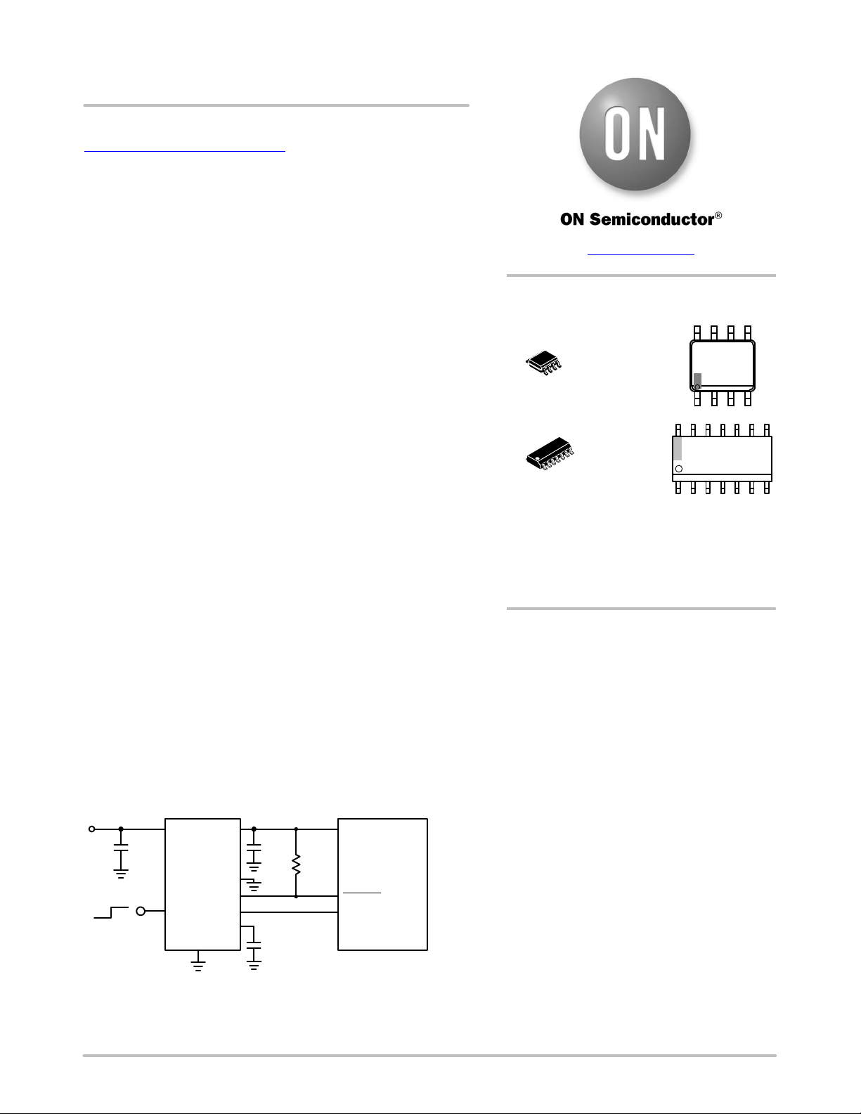
Typical Applications
• Body Control Module
• Instruments and Clusters
• Occupant Protection and Comfort
• Powertrain
V
in
100 nF
OFF
ON
*−optional if Reset function is needed
© Semiconductor Components Industries, LLC, 2015
September, 2019 − Rev. 1
V
C
in
NCV4263−2C
EN
Figure 1. Application Schematic
in
GND
V
out
RADJ
RO
WDI
D
C
out
22 mF
C
100 nF
D
RRO*
5.6 kW
V
DD
Microprocessor
RESET
I/O
1 Publication Order Number:
NCV4263−2C/D
Page 2
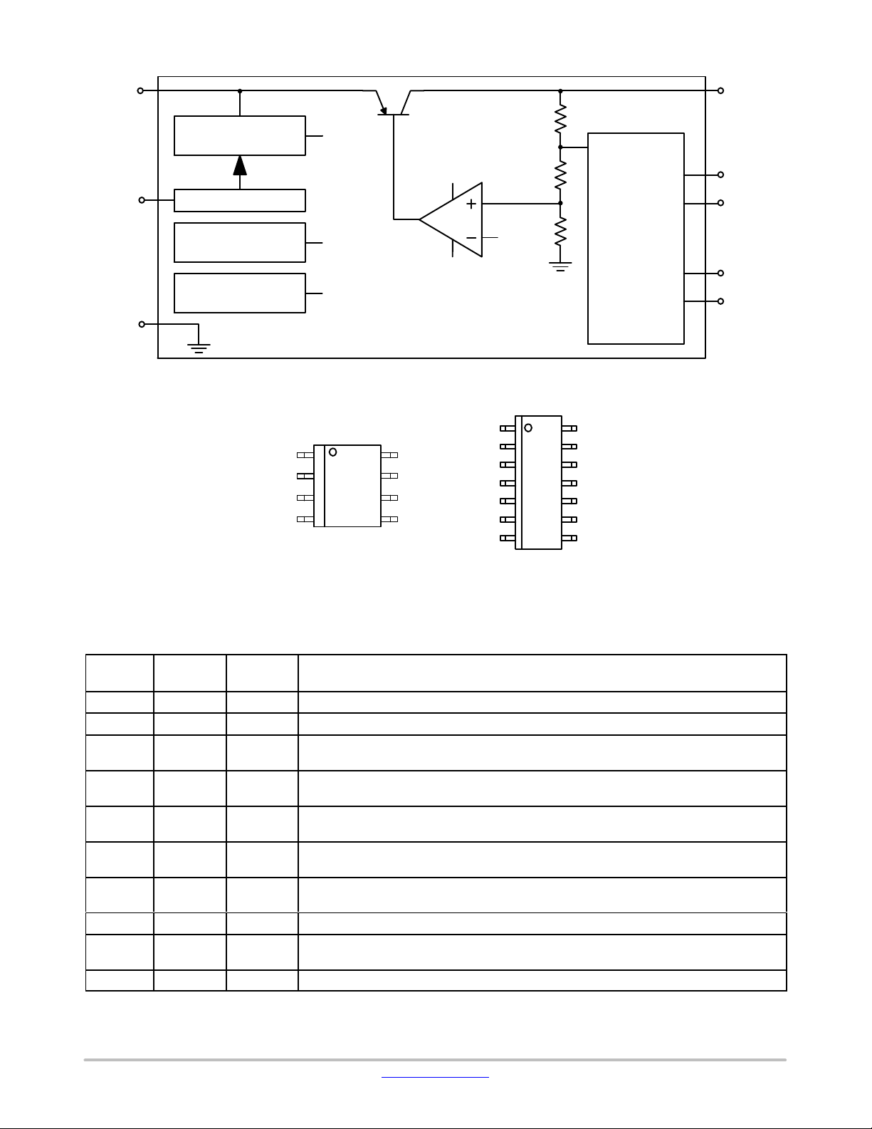
NCV4263−2C
V
EN
GND
V
in
VOLTAGE
REFERENCE
V
REF
SP
ENABLE
out
RO
WDI
RESET
SATURATION
PROTECTION
THERMAL
SHUTDOWN
SP
TSD
TSD
V
REF
GENERATOR
and
WATCHDOG
D
RADJ
Figure 2. Simplified Block Diagram
114
18
Vin
EN
RO
GND
SOIC−8 EP
Vout
WDI
RADJ
D
RO
NC
GND
GND GND
GND
D
RADJ
EN
Vin
GND
GND
Vout
WDI
SOIC−14
Figure 3. Pin Connections
(Top View)
PIN FUNCTION DESCRIPTION
Pin No.
SO−8 EP
1 13 V
2 14 EN Enable Input. Low level disables the chip. Connect to Vin if this function is not needed.
3 1 RO
4
5 6 D
6 7 RADJ
7 8 WDI
8 9 V
EPAD −
− 2 NC Not connected. No internally bonded.
Pin No.
SO−14
3, 4, 5,
10, 11, 12
Pin Name Description
in
Positive Power Supply. Connect ceramic capacitor to ground.
Reset Output; Open Collector connected to the V
leave open if the function is not needed
via an internal 30 kW pull−up resistor;
out
GND Power Supply Ground. Connect pins to heat sink area with GND potential.
DelayTiming. Connect to GND via ceramic capacitor for adjusting reset delay timing and
watchdog trigger time or leave open if this function is not needed.
Reset Adjust Threshold. Connect to GND (VRT = 93% of V
adjust the reset threshold.
) or to output voltage divider to
out
Watchdog Input. Rising edge triggered Input for watchdog pulses. Connect to GND if this
function is not needed.
out
Exposed
Pad
Regulated Output Voltage. Connect a C
Connect to ground potential or leave unconnected.
≥ 22 mF capacitor to ground.
out
www.onsemi.com
2
Page 3
NCV4263−2C
ABSOLUTE MAXIMUM RATINGS
Rating Symbol Min Max Unit
Input Voltage (Note 1) V
Enable Input V
Output Voltage V
Reset Output Voltage V
Watchdog Input Voltage V
Reset Adjust Threshold V
Delay Timing Output Voltage V
Maximum Junction Temperature T
Storage Temperature T
in
EN
out
RO
WDI
RADJ
D
J
STG
Stresses exceeding those listed in the Maximum Ratings table may damage the device. If any of these limits are exceeded, device functionality
should not be assumed, damage may occur and reliability may be affected.
1. Refer to ELECTRICAL CHARACTERISTICS and APPLICATION INFORMATION for Safe Operating Area.
ESD CAPABILITY (Note 2)
Rating Symbol Min Max Unit
ESD Capability, Human Body Model ESD
ESD Capability, Charged Device Model ESD
2. This device series incorporates ESD protection and is tested by the following methods:
ESD Human Body Model tested per AEC−Q100−002 (JS−001−2010)
ESD Charged Device Model tested per AEC−Q100−011 (EIA/JESD22−C101)
HBM
CDM
−42 45 V
−42 45 V
−1 7 V
−0.3 7 V
−0.3 7 V
−0.3 7 V
−0.3 7 V
−40 150 °C
−55 150 °C
− 2 kV
− 1 kV
LEAD SOLDERING TEMPERATURE AND MSL (Note 3)
Rating
Moisture Sensitivity Level
SOIC−14
SOIC−8 EP
Lead Temperature Soldering
Reflow (SMD Styles Only), Pb−Free Versions
3. For more information, please refer to our Soldering and Mounting Techniques Reference Manual, SOLDERRM/D
Symbol Min Max Unit
MSL
1
2
T
SLD
− 265 peak
THERMAL CHARACTERISTICS
Rating Symbol Value Unit
Thermal Characteristics, SOIC−8 Exposed Pad (Note 4)
Thermal Resistance, Junction−to−Air (Note 5)
Thermal Reference, Junction−to−Pad (Note 5)
Y
R
θJA
ψJPad
65.1
8.7
Thermal Characteristics, SOIC−14 (Note 4)
Thermal Resistance, Junction−to−Air (Note 5)
Thermal Reference, Junction−to−Pin4 (Note 5)
4. Refer to ELECTRICAL CHARACTERISTICS and APPLICATION INFORMATION for Safe Operating Area.
5. Values based on copper area of 645 mm
2
(or 1 in2) of 1 oz copper thickness and FR4 PCB substrate.
Y
R
θJA
ψJP4
94.8
18.3
OPERATING RANGES (Note 6)
Rating
Input Voltage V
Junction Temperature T
6. Refer to ELECTRICAL CHARACTERISTICS and APPLICATION INFORMATION for Safe Operating Area.
Symbol Min Max Unit
in
J
5.5 40 V
−40 150 °C
−
°C
°C/W
°C/W
www.onsemi.com
3
Page 4
NCV4263−2C
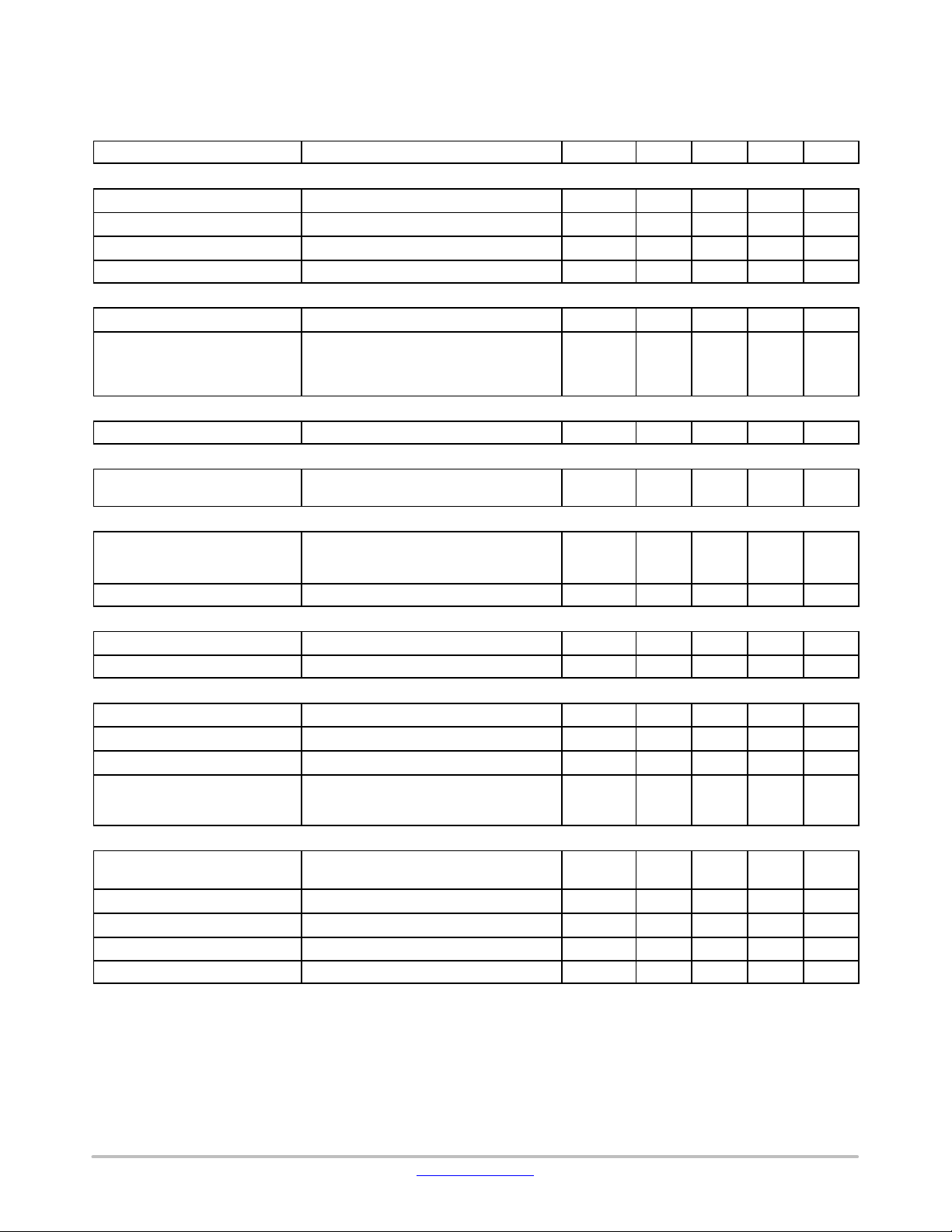
ELECTRICAL CHARACTERISTICS V
f
= 1 kHz. Min and Max values are valid for temperature range *40°C v TJ v 150°C unless otherwise noted and are guaranteed by
WDI
test design or statistical correlation. Typical values are referenced to T
Parameter
= 13.5 V, VEN = 5 V, Cin = 100 nF, C
in
= 25°C. (Notes 7 and 8)
J
Test Conditions Symbol Min Typ Max Unit
= 22 mF, ESR = 1.5 W, WDI = 5 V pulses,
out
REGULATOR OUTPUT
Output Voltage Accuracy
Line Regulation I
Load Regulation I
Dropout Voltage (Note 9) I
Vin = 6 V to 40 V, I
= 150 mA, Vin = 6 V to 28 V Reg
out
= 5 mA to 150 mA Reg
out
= 150 mA V
out
= 5 to 150 mA V
out
out
DO
line
load
4.90 5.0 5.10 V
−25 3 25 mV
−25 − 25 mV
− 300 500 mV
DISABLE AND QUIESCENT CURRENTS
Disable Current
Quiescent Current, Iq = Iin − I
out
VEN = 0 V,TJ < 125°C I
I
= 0 mA
out
I
= 150 mA
out
I
= 150 mA, Vin = 4.5 V
out
DIS
I
q
− 0.066 10
−
0.275
−
−
3
11.3
1.3
18
23
mA
mA
CURRENT LIMIT PROTECTION
Current Limit
= 0.96 x V
out
out_nom
I
LIM
200 418 500 mA
V
PSRR
Power Supply Ripple Rejection
(Note 10)
f = 100 Hz, 0.5 V
p−p
PSRR − 80 − dB
ENABLE
Enable Input Threshold Voltage
Logic High
Logic Low
V
w 0.9 x V
out
V
v 0.1 V
out
out_nom
V
Enable Input Current VEN = 5 V I
th(EN)
EN
−
0.8
2.0
1.74
5 10 25
3.5
−
V
mA
WATCHDOG INPUT
Watchdog Input Low Time
CD = 100 nF, V
Watchdog Trigger Time CD = 100 nF, V
> VRT, no WDI signal t
out
> VRT, no WDI signal t
out
WL
WTT
1 2 3.5 ms
16 20.8 27 ms
DELAY TIMING
Charge Current
VD = 1 V, no WDI signal I
Discharge Current VD = 1 V, no WDI signal I
Saturation Voltage V
< VRT, no WDI signal V
out
Switching Threshold
Upper
Lower
D_charge
D_disch
D_sat
V
thH(D)
V
thL(D)
40 66.8 95
4.40 6.54 9.40
− 6 100 mV
1.45
0.2
1.70
0.34
2.05
0.55
mA
mA
V
RESET OUTPUT
V
Output Voltage Reset Threshold
(Note 11)
Reset Adjust Threshold (70% of V
decreasing, V
out
out_nom
Reset Adjustment Range (Note 12) V
Reset Output Low Voltage IRO = 1 mA V
Reset Delay Time CD = 100 nF t
= 0 V V
RADJ
) v V
< (VRT) V
out
RT
th(RADJ)
RT_range
ROL
RD
90 93 96 % V
1.26 1.36 1.44 V
70 − 93 % V
− 0.01 0.4 V
1.3 2.6 4.1 ms
out
out
Product parametric performance is indicated in the Electrical Characteristics for the listed test conditions, unless otherwise noted. Product performance may not be indicated by the Electrical Characteristics if operated under different conditions.
7. Refer to ABSOLUTE MAXIMUM RATINGS and APPLICATION INFORMATION for Safe Operating Area.
8. Performance guaranteed over the indicated operating temperature range by design and/or characterization tested at T
cycle pulse techniques are used during testing to maintain the junction temperature as close to ambient as possible.
9. Measured when output voltage falls 100 mV below the regulated voltage at V
10.Values based on design and/or characterization.
= 13.5 V.
in
[TJ. Low duty
A
11.See APPLICATION INFORMATION section for Reset Threshold Adjustment
12.V
limits are guaranteed by VRT and V
RT_range
th(RADJ)
parameters.
www.onsemi.com
4
Page 5

NCV4263−2C
ELECTRICAL CHARACTERISTICS V
f
= 1 kHz. Min and Max values are valid for temperature range *40°C v TJ v 150°C unless otherwise noted and are guaranteed by
WDI
test design or statistical correlation. Typical values are referenced to T
= 13.5 V, VEN = 5 V, Cin = 100 nF, C
in
= 25°C. (Notes 7 and 8)
J
= 22 mF, ESR = 1.5 W, WDI = 5 V pulses,
out
Parameter UnitMaxTypMinSymbolTest Conditions
RESET OUTPUT
Reset Reaction Time
CD = 100 nF t
RR
0.5 1.2 4
ms
THERMAL SHUTDOWN
Thermal Shutdown Temperature
(Note 10)
I
= 1 mA T
out
SD
150 177 195 °C
Product parametric performance is indicated in the Electrical Characteristics for the listed test conditions, unless otherwise noted. Product performance may not be indicated by the Electrical Characteristics if operated under different conditions.
7. Refer to ABSOLUTE MAXIMUM RATINGS and APPLICATION INFORMATION for Safe Operating Area.
8. Performance guaranteed over the indicated operating temperature range by design and/or characterization tested at T
cycle pulse techniques are used during testing to maintain the junction temperature as close to ambient as possible.
9. Measured when output voltage falls 100 mV below the regulated voltage at V
10.Values based on design and/or characterization.
= 13.5 V.
in
[TJ. Low duty
A
11.See APPLICATION INFORMATION section for Reset Threshold Adjustment
12.V
limits are guaranteed by VRT and V
RT_range
th(RADJ)
parameters.
www.onsemi.com
5
Page 6

NCV4263−2C
TYPICAL CHARACTERISTICS
0.32
Vin = 13.5 V
= 0 mA
0.30
I
out
0.28
0.26
0.24
0.22
, QUIESCENT CURRENT (mA)
q
I
0.20
40 120 160
TJ, TEMPERATURE (°C) Vin, INPUT VOLTAGE (V)
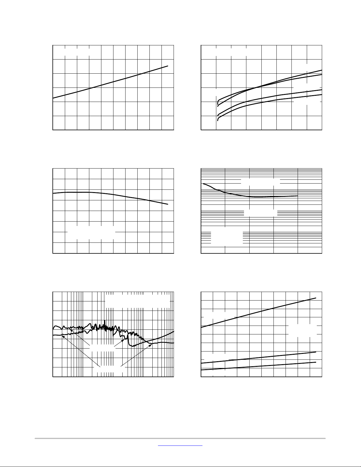
Figure 4. Quiescent Current vs. Temperature Figure 5. Quiescent Current vs. Input Voltage
10
9
Vin = 13.5 V
= 25°C
T
8
J
7
6
5
4
3
2
, QUIESCENT CURRENT (mA)
q
I
1
0
I
, OUTPUT CURRENT (mA) TJ, TEMPERATURE (°C)
out
Figure 6. Quiescent Current vs. Output
Current
16
14
TJ = 25°C
R
= 25 W
out
12
10
8
6
4
, QUIESCENT CURRENT (mA)
q
2
I
0
1401008060200−20−40
35302520151050
40
5.10
5.08
5.06
Vin = 13.5 V
= 5 mA
I
out
5.04
5.02
5.00
4.98
4.96
, OUTPUT VOLTAGE (V)
4.94
out
V
4.92
4.90
250200150100500
40 120 160
1401008060200−20−40
Figure 7. Output Voltage Accuracy
6
5
4
3
2
, OUTPUT VOLTAGE (V)
out
1
V
0
600
TJ = 150°C
TJ = 25°C
R
= 25 W
out
500
400
300
200
, DROPOUT VOLTAGE (mV)
100
DO
V
TJ = 125°C
TJ = 25°C
TJ = −40°C
0
6543210
Vin, INPUT VOLTAGE (V) I
, OUTPUT CURRENT (mA)
out
Figure 8. Output Voltage vs. Input Voltage Figure 9. Dropout Voltage vs. Output Current
www.onsemi.com
6
250200150100500
Page 7
NCV4263−2C
TYPICAL CHARACTERISTICS
600
I
= 150 mA
out
500
400
300
200
, DROPOUT VOLTAGE (mV)
100
DO
V
0
40 120 160
TJ, TEMPERATURE (°C) Vin, INPUT VOLTAGE (V)
Figure 10. Dropout Voltage vs. Temperature Figure 11. Output Current Limit vs. Input
550
500
450
400
350
300
250
, OUTPUT CURRENT LIMIT (mA)
200
LIM
I
150
Vin = 13.5 V
= 0.96 x V
V
out
out_nom
20 120 160
TJ, TEMPERATURE (°C) I
Figure 12. Output Current Limit vs.
Temperature
600
V
= 0.96 x V
out
out_nom
550
TJ = 25°C
500
450
TJ = 125°C
TJ = −40°C
400
350
, OUTPUT CURRENT LIMIT (mA)
LIM
I
300
1401008060200−20−40
TJ = 150°C
35302520151050
40
Voltage
100
Unstable Region
10
1
Vin = 13.5 V
C
= 22 mF
out
T
= 25°C
J
ESR, OUTPUT CAPACITOR ESR (W)
0.1
0.01
1401008060400−20−40
Stable Region
, OUTPUT CURRENT (mA)
out
250200150100500
Figure 13. Output Capacitor ESR Stability
Region vs. Output Current
120
110
100
90
80
70
PSRR (dB)
60
50
40
30
Vin = 13.5 V DC + 0.5 Vpp AC
C
= 22 mF, TA = 25°C
out
45
40
VEN = 13.5 V
35
30
25
Vin = 13.5 V
= 0 mA
I
out
20
50
I
= 1 mA
out
I
out
= 100 mA
100,00010,000100010010
, ENABLE INPUT CURRENT (mA)
EN
I
15
10
5
0
VEN = 5 V
VEN = 3.3 V
12040 60
FREQUENCY (Hz) TJ, TEMPERATURE (°C)
Figure 14. PSRR vs. Frequency Figure 15. Enable Input Current vs.
Temperature
www.onsemi.com
7
16014010080200−20−40
Page 8

NCV4263−2C
TYPICAL CHARACTERISTICS
1.44
1.42
1.40
1.38
1.36
1.34
1.32
1.30
, RESET ADJUST THRESHOLD (V)V
1.28
1.26
th(RADJ)
V
Vin = 13.5 V
= 0.7 x V
V
out
40 120 160
TJ, TEMPERATURE (°C) V
Figure 16. Reset Adjust Threshold vs.
Temperature
1.8
1.6
Upper Threshold
1.4
1.2
1.0
Vin = 13.5 V
0.8
0.6
0.4
, RESET DELAY THRESHOLDS (V)
0.2
th(D)
0
Lower Threshold
20 100 160
TJ, TEMPERATURE (°C) TJ, TEMPERATURE (°C)
Figure 18. Delay Timing Switching Thresholds
vs. Temperature
out_nom
1.44
1.42
1.40
1.38
1.36
1.34
1.32
1.30
, RESET ADJUST THRESHOLD (V)
Vin = 13.5 V
= 25°C
T
J
1.28
1.26
1401008060200−20−40
th(RADJ)
V
, OUTPUT VOLTAGE (V)
out
5.04.54.03.53.02.52.0
Figure 17. Reset Adjust Threshold vs. Output
Voltage
80
70
Charge Current
60
50
, RESET DELAY
(disch)
40
30
Vin = 13.5 V
= 1 V
V
D
20
D(charge),
I
10
0
1401208060400−20−40
CHARGE / DISCHARGE CURRENT (mA)
Discharge Current
20 120 160
1401008060400−20−40
Figure 19. Reset Delay Charge / Discharge
Current vs. Temperature
27
26
25
24
23
22
21
20
19
18
, WATCHDOG TRIGGER TIME (ms)
17
WTT
t
16
40 120 160
TJ, TEMPERATURE (°C)
Figure 20. Watchdog Trigger Time vs.
Temperature
www.onsemi.com
Vin = 13.5 V
> V
V
out
RT
CD = 100 nF
no WDI signal
1401008060200−20−40
8
Page 9

V
NCV4263−2C
in
V
V
V
V
1 V
V
thH(D)
thL(D)
V
V
out
RT
D
RO
1 V
ROL
t
RD
Thermal
Shutdown
t
RD
Voltage Dip
Input
t
Under
Voltage
RR
Figure 21. Reset Operation Timing Diagram
Output
Voltage Spike
t < t
Overload
RR
t
t
t
t
V
WDI
V
D
V
thH(D)
V
thL(D)
V
RO
V
ROL
t
WTT
t
WL
t
WP
t
t
t
Figure 22. Watchdog Operation Timing Diagram
www.onsemi.com
9
Page 10

NCV4263−2C
DEFINITIONS
General
All measurements are performed using short pulse low
duty cycle techniques to maintain junction temperature as
close as possible to ambient temperature.
Output Voltage
The output voltage parameter is defined for specific
temperature, input voltage and output current values or
specified over Line, Load and Temperature ranges.
Line Regulation
The change in output voltage for a change in input voltage
measured for specific output current over operating ambient
temperature range.
Load Regulation
The change in output voltage for a change in output
current measured for specific input voltage over operating
ambient temperature range.
Dropout Voltage
The input to output differential at which the regulator
output no longer maintains regulation against further
reductions in input voltage. It is measured when the output
drops 100 mV below its nominal value. The junction
temperature, load current, and minimum input supply
requirements affect the dropout level.
Quiescent and Disable Currents
Quiescent Current (Iq) is the difference between the input
current (measured through the LDO input pin) and the
output load current. If Enable pin is set to LOW the regulator
reduces its internal bias and shuts off the output, this term is
called the disable current (I
DIS
).
Current Limit and Short Circuit Current Limit
Current Limit is value of output current by which output
voltage drops below 96% of its nominal value. It means that
the device is capable to supply minimum 200 mA without
sending Reset signal to microprocessor.
Short Circuit Current Limit is output current value
measured with output of the regulator shorted to ground.
PSRR
Power Supply Rejection Ratio is defined as ratio of output
voltage and input voltage ripple. It is measured in decibels
(dB).
Line Transient Response
Typical output voltage overshoot and undershoot
response when the input voltage is excited with a given
slope.
Load Transient Response
Typical output voltage overshoot and undershoot
response when the output current is excited with a given
slope between low−load and high−load conditions.
Thermal Protection
Internal thermal shutdown circuitry is provided to protect
the integrated circuit in the event that the maximum junction
temperature is exceeded. When activated at typically 177°C,
the regulator turns off. This feature is provided to prevent
failures from accidental overheating.
Maximum Package Power Dissipation
The power dissipation level is maximum allowed power
dissipation for particular package or power dissipation at
which the junction temperature reaches its maximum
operating value, whichever is lower.
www.onsemi.com
10
Page 11

NCV4263−2C
APPLICATIONS INFORMATION
The NCV4263−2C regulator is self−protected with
internal thermal shutdown and internal current limit. Typical
characteristics are shown in Figures 4 to 22.
Input Decoupling (Cin)
A ceramic or tantalum 0.1 mF capacitor is recommended
and should be connected close to the NCV4263−2C
package. Higher capacitance and lower ESR will improve
the overall line and load transient response. If extremely fast
input voltage transients are expected then appropriate input
filter is recommended to use in order to decrease rising
and/or falling edges below 50 V/ms for proper operation.
The filter can be composed of several capacitors in parallel.
Output Decoupling (C
out
)
The NCV4263−2C is a stable component and requires a
minimum Equivalent Series Resistance (ESR) for the output
capacitor. Stability region of ESR versus Output Current is
shown in Figure 13. The minimum output decoupling value
is 22 mF and can be augmented to fulfill stringent load
transient requirements. Larger values improve noise
rejection and load transient response.
Enable Operation
The Enable pin will turn the regulator on or off. The
threshold limits are covered in the electrical characteristics
table in this data sheet.
Delay Timing
The Delay Timing pin is current source. Current from
Delay Timing pin charges connected capacitor. The value of
this capacitor determines the Reset Delay Time by
Equation 1 and Watchdog Trigger Time by Equation 4.
t
CD+
ǒ
RD_des
t
RD
Ǔ
100 nF
(eq. 1)
where:
C
D
t
RD_des
t
RD
is capacitance of Delay capacitor
is desired Reset Delay Time
is Reset Delay Time specified in
datasheet
Reset Operation
A reset signal is provided on the Reset Output pin to
provide feedback to the microprocessor of an out of
regulation condition. The timing diagram of reset function
is shown in Figure 21. This is in the form of a logic signal on
Reset Output. Output voltage conditions below the Reset
Threshold causes Reset Output to go low. The Reset Output
integrity is maintained down to V
= 1.0 V. The Reset
out
Output circuitry is open collector output with internal 30 kW
pull−up resistor. Leave open this output if the Reset function
is not needed else an external pull−up resistor (5.6 kW)
connect to the output (V
out
).
Reset Threshold is default set to 93% of nominal Output
Voltage (V
= 0 V). Reset Threshold can be varied in
RADJ
range of Output Voltage 70% ≤ V
< VRT by external
out
resistor output voltage divider, see schematic on Figure 23
and specification of Reset Output.
V
V
in
C
in
100 nF
NCV4263−2C
OFF
ON
Figure 23. Application Schematic with Adjustable
EN
out
C
22 mF
RADJ
RO
WDI
D
GND
Reset Threshold
out
C
D
100 nF
R
RADJ1
R
RADJ2
R
RO
5.6 kW
V
DD
Microprocessor
RESET
I/O
Desired Reset Threshold is given by Equation 2.
V
RT_des
+
R
ǒ
RADJ1
R
) R
RADJ2
RADJ2
Ǔ
V
th(RADJ)
(eq. 2)
where:
V
RT_ des
R
RADJ1
V
th(RADJ)
, R
is desired Reset Threshold
are resistance of resistor divider
RADJ2
is Reset Adjust Threshold specified in
datasheet
Use R
≤ 50 kW to avoid significant Reset Threshold
RADJ2
error due to RADJ bias current.
Watchdog Operation
Watchdog Input monitors a signal from microprocessor.
This input is positive edge sensitive. The timing diagram of
watchdog function is shown in Figure 22. When watchdog
signal is not received during Watchdog Trigger Time, Reset
Output goes low for a Watchdog Input Low Time and is
periodically generated with period given by Equation 3.
Capacitance of Delay capacitor for setting the desired
Watchdog Trigger Time is given by Equation 4.
tWP+ tWL) t
ǒ
CD+
t
WTT_des
t
WTT
WTT
Ǔ
100 nF
(eq. 3)
(eq. 4)
where:
C
D
t
WTT_des
t
WTT
is capacitance of Delay capacitor
is desired Watchdog Trigger Time
is Watchdog Trigger Time specified in
datasheet
t
WL
t
WP
Thermal Considerations
is Watchdog Input Low Time
is Watchdog Input Period
As power in the NCV4263−2C increases, it might become
necessary to provide some thermal relief. The maximum
power dissipation supported by the device is dependent
www.onsemi.com
11
Page 12

NCV4263−2C
upon board design and layout. Mounting pad configuration
on the PCB, the board material, and the ambient temperature
affect the rate of junction temperature rise for the part. When
the NCV4263−2C has good thermal conductivity through
the PCB, the junction temperature will be relatively low with
high power applications. The maximum dissipation the
NCV4263−2C can handle is given by:
P
D(MAX)
+
ƪ
T
J(MAX)
R
qJA
* T
ƫ
A
(eq. 5)
Since TJ is not recommended to exceed 150°C, then the
NCV4263−2C soldered on 645 mm
2
, 1 oz copper area, FR4
can dissipate up to 1.3 W in SOIC−14 package and 1.9 W in
SOIC−8 EP package, when the ambient temperature (T
25°C. See Figures 24 and 25 for R
versus PCB area. The
JA
q
) is
A
power dissipated by the NCV4263−2C can be calculated
from the following equations:
PD[ V
in
ǒ
Iq@I
out
ǒ
Ǔ
) I
Vin* V
out
out
Ǔ
(eq. 6)
or
I
out
Ǔ
(eq. 7)
Hints
V
in(MAX)
[
P
D(MAX)
)ǒV
I
out
) I
out
q
Vin and GND printed circuit board traces should be as
wide as possible. When the impedance of these traces is
high, there is a chance to pick up noise or cause the regulator
to malfunction. Place external components, especially the
output capacitor, as close as possible to the NCV4263−2C
and make traces as short as possible.
160
150
140
130
120
110
100
90
80
70
, THERMAL RESISTANCE (°C/W)
JA
60
q
R
50
SOIC−14 − 1 OZ Cu
SOIC−14 − 2 OZ Cu
300 600
COPPER HEAT SPREADER AREA (mm2)
7005004002001000
Figure 24. Thermal Resistance vs. PCB Copper Area
for SOIC−14
160
150
140
130
120
110
100
90
80
70
, THERMAL RESISTANCE (°C/W)
JA
60
q
R
50
SOIC−8 EP − 1 OZ Cu
SOIC−8 EP − 2 OZ Cu
300 600
COPPER HEAT SPREADER AREA (mm2)
7005004002001000
Figure 25. Thermal Resistance vs. PCB Copper Area
for SOIC−8 EP
ORDERING INFORMATION
Device Output Voltage Marking Package Shipping
NCV4263−2CD250R2G 5.0 V NCV4263−2C50G SOIC−14
(Pb−Free)
NCV4263−2CPD50R2G 5.0 V V632C5 SOIC−8 EP
(Pb−Free)
†For information on tape and reel specifications, including part orientation and tape sizes, please refer to our Tape and Reel Packaging
Specifications Brochure, BRD8011/D.
2500 / Tape & Reel
2500 / Tape & Reel
†
www.onsemi.com
12
Page 13

MECHANICAL CASE OUTLINE
PACKAGE DIMENSIONS
14
1
SCALE 1:1
SOIC−14 NB
CASE 751A−03
ISSUE L
DATE 03 FEB 2016
14
H
M
0.25 B
0.10
14X
0.58
D
M
13X
e
SOLDERING FOOTPRINT*
6.50
1
A
B
8
E
71
b
M
0.25 B
S
A
C
A
A1
SEATING
C
PLANE
14X
1.18
S
1.27
PITCH
DETAIL A
h
X 45
_
NOTES:
1. DIMENSIONING AND TOLERANCING PER
ASME Y14.5M, 1994.
2. CONTROLLING DIMENSION: MILLIMETERS.
3. DIMENSION b DOES NOT INCLUDE DAMBAR
A3
L
DETAIL A
M
PROTRUSION. ALLOWABLE PROTRUSION
SHALL BE 0.13 TOTAL IN EXCESS OF AT
MAXIMUM MATERIAL CONDITION.
4. DIMENSIONS D AND E DO NOT INCLUDE
MOLD PROTRUSIONS.
5. MAXIMUM MOLD PROTRUSION 0.15 PER
SIDE.
DIM MIN MAX MIN MAX
A 1.35 1.75 0.054 0.068
A1 0.10 0.25 0.004 0.010
A3 0.19 0.25 0.008 0.010
b 0.35 0.49 0.014 0.019
D 8.55 8.75 0.337 0.344
E 3.80 4.00 0.150 0.157
e 1.27 BSC 0.050 BSC
H 5.80 6.20 0.228 0.244
h 0.25 0.50 0.010 0.019
L 0.40 1.25 0.016 0.049
M 0 7 0 7
__ __
INCHESMILLIMETERS
GENERIC
MARKING DIAGRAM*
14
XXXXXXXXXG
AWLYWW
1
XXXXX = Specific Device Code
A = Assembly Location
WL = Wafer Lot
Y = Year
WW = Work Week
G = Pb−Free Package
*This information is generic. Please refer to
device data sheet for actual part marking.
Pb−Free indicator, “G” or microdot “ G”,
may or may not be present.
DIMENSIONS: MILLIMETERS
*For additional information on our Pb−Free strategy and soldering
details, please download the ON Semiconductor Soldering and
Mounting Techniques Reference Manual, SOLDERRM/D.
STYLES ON PAGE 2
DOCUMENT NUMBER:
DESCRIPTION:
ON Semiconductor and are trademarks of Semiconductor Components Industries, LLC dba ON Semiconductor or its subsidiaries in the United States and/or other countries.
ON Semiconductor reserves the right to make changes without further notice to any products herein. ON Semiconductor makes no warranty, representation or guarantee regarding
the suitability of its products for any particular purpose, nor does ON Semiconductor assume any liability arising out of the application or use of any product or circuit, and specifically
disclaims any and all liability, including without limitation special, consequential or incidental damages. ON Semiconductor does not convey any license under its patent rights nor the
rights of others.
© Semiconductor Components Industries, LLC, 2019
98ASB42565B
SOIC−14 NB
Electronic versions are uncontrolled except when accessed directly from the Document Repository.
Printed versions are uncontrolled except when stamped “CONTROLLED COPY” in red.
PAGE 1 OF 2
www.onsemi.com
Page 14

SOIC−14
CASE 751A−03
ISSUE L
DATE 03 FEB 2016
STYLE 1:
PIN 1. COMMON CATHODE
2. ANODE/CATHODE
3. ANODE/CATHODE
4. NO CONNECTION
5. ANODE/CATHODE
6. NO CONNECTION
7. ANODE/CATHODE
8. ANODE/CATHODE
9. ANODE/CATHODE
10. NO CONNECTION
11. ANODE/CATHODE
12. ANODE/CATHODE
13. NO CONNECTION
14. COMMON ANODE
STYLE 5:
PIN 1. COMMON CATHODE
2. ANODE/CATHODE
3. ANODE/CATHODE
4. ANODE/CATHODE
5. ANODE/CATHODE
6. NO CONNECTION
7. COMMON ANODE
8. COMMON CATHODE
9. ANODE/CATHODE
10. ANODE/CATHODE
11. ANODE/CATHODE
12. ANODE/CATHODE
13. NO CONNECTION
14. COMMON ANODE
STYLE 2:
CANCELLED
STYLE 6:
PIN 1. CATHODE
2. CATHODE
3. CATHODE
4. CATHODE
5. CATHODE
6. CATHODE
7. CATHODE
8. ANODE
9. ANODE
10. ANODE
11. ANODE
12. ANODE
13. ANODE
14. ANODE
STYLE 3:
PIN 1. NO CONNECTION
2. ANODE
3. ANODE
4. NO CONNECTION
5. ANODE
6. NO CONNECTION
7. ANODE
8. ANODE
9. ANODE
10. NO CONNECTION
11. ANODE
12. ANODE
13. NO CONNECTION
14. COMMON CATHODE
STYLE 7:
PIN 1. ANODE/CATHODE
2. COMMON ANODE
3. COMMON CATHODE
4. ANODE/CATHODE
5. ANODE/CATHODE
6. ANODE/CATHODE
7. ANODE/CATHODE
8. ANODE/CATHODE
9. ANODE/CATHODE
10. ANODE/CATHODE
11. COMMON CATHODE
12. COMMON ANODE
13. ANODE/CATHODE
14. ANODE/CATHODE
STYLE 4:
PIN 1. NO CONNECTION
2. CATHODE
3. CATHODE
4. NO CONNECTION
5. CATHODE
6. NO CONNECTION
7. CATHODE
8. CATHODE
9. CATHODE
10. NO CONNECTION
11. CATHODE
12. CATHODE
13. NO CONNECTION
14. COMMON ANODE
STYLE 8:
PIN 1. COMMON CATHODE
2. ANODE/CATHODE
3. ANODE/CATHODE
4. NO CONNECTION
5. ANODE/CATHODE
6. ANODE/CATHODE
7. COMMON ANODE
8. COMMON ANODE
9. ANODE/CATHODE
10. ANODE/CATHODE
11. NO CONNECTION
12. ANODE/CATHODE
13. ANODE/CATHODE
14. COMMON CATHODE
DOCUMENT NUMBER:
DESCRIPTION:
ON Semiconductor and are trademarks of Semiconductor Components Industries, LLC dba ON Semiconductor or its subsidiaries in the United States and/or other countries.
ON Semiconductor reserves the right to make changes without further notice to any products herein. ON Semiconductor makes no warranty, representation or guarantee regarding
the suitability of its products for any particular purpose, nor does ON Semiconductor assume any liability arising out of the application or use of any product or circuit, and specifically
disclaims any and all liability, including without limitation special, consequential or incidental damages. ON Semiconductor does not convey any license under its patent rights nor the
rights of others.
© Semiconductor Components Industries, LLC, 2019
98ASB42565B
SOIC−14 NB
Electronic versions are uncontrolled except when accessed directly from the Document Repository.
Printed versions are uncontrolled except when stamped “CONTROLLED COPY” in red.
PAGE 2 OF 2
www.onsemi.com
Page 15

MECHANICAL CASE OUTLINE
PACKAGE DIMENSIONS
8
1
SCALE 1:1
SOIC−8 EP
CASE 751AC
ISSUE D
DATE 02 APR 2019
GENERIC
MARKING DIAGRAM*
8
XXXXX
AYWWG
G
1
DOCUMENT NUMBER:
DESCRIPTION:
ON Semiconductor and are trademarks of Semiconductor Components Industries, LLC dba ON Semiconductor or its subsidiaries in the United States and/or other countries.
ON Semiconductor reserves the right to make changes without further notice to any products herein. ON Semiconductor makes no warranty, representation or guarantee regarding
the suitability of its products for any particular purpose, nor does ON Semiconductor assume any liability arising out of the application or use of any product or circuit, and specifically
disclaims any and all liability, including without limitation special, consequential or incidental damages. ON Semiconductor does not convey any license under its patent rights nor the
rights of others.
© Semiconductor Components Industries, LLC, 2018
XXXXXX = Specific Device Code
A = Assembly Location
Y = Year
WW = Work Week
G = Pb−Free Package
98AON14029D
SOIC−8 EP
Electronic versions are uncontrolled except when accessed directly from the Document Repository.
Printed versions are uncontrolled except when stamped “CONTROLLED COPY” in red.
*This information is generic. Please refer to
device data sheet for actual part marking.
Pb−Free indicator, “G” or microdot “ G”, may
or may not be present and may be in either
location. Some products may not follow the
Generic Marking.
PAGE 1 OF 1
www.onsemi.com
Page 16

ON Semiconductor and are trademarks of Semiconductor Components Industries, LLC dba ON Semiconductor or its subsidiaries in the United States and/or other countries.
ON Semiconductor owns the rights to a number of patents, trademarks, copyrights, trade secrets, and other intellectual property. A listing of ON Semiconductor’s product/patent
coverage may be accessed at www.onsemi.com/site/pdf/Patent−Marking.pdf
ON Semiconductor makes no warranty, representation or guarantee regarding the suitability of its products for any particular purpose, nor does ON Semiconductor assume any liability
arising out of the application or use of any product or circuit, and specifically disclaims any and all liability, including without limitation special, consequential or incidental damages.
Buyer is responsible for its products and applications using ON Semiconductor products, including compliance with all laws, regulations and safety requirements or standards,
regardless of any support or applications information provided by ON Semiconductor. “Typical” parameters which may be provided in ON Semiconductor data sheets and/or
specifications can and do vary in different applications and actual performance may vary over time. All operating parameters, including “Typicals” must be validated for each customer
application by customer’s technical experts. ON Semiconductor does not convey any license under its patent rights nor the rights of others. ON Semiconductor products are not
designed, intended, or authorized for use as a critical component in life support systems or any FDA Class 3 medical devices or medical devices with a same or similar classification
in a foreign jurisdiction or any devices intended for implantation in the human body. Should Buyer purchase or use ON Semiconductor products for any such unintended or unauthorized
application, Buyer shall indemnify and hold ON Semiconductor and its officers, employees, subsidiaries, affiliates, and distributors harmless against all claims, costs, damages, and
expenses, and reasonable attorney fees arising out of, directly or indirectly, any claim of personal injury or death associated with such unintended or unauthorized use, even if such
claim alleges that ON Semiconductor was negligent regarding the design or manufacture of the part. ON Semiconductor is an Equal Opportunity/Affirmative Action Employer. This
literature is subject to all applicable copyright laws and is not for resale in any manner.
. ON Semiconductor reserves the right to make changes without further notice to any products herein.
PUBLICATION ORDERING INFORMATION
LITERATURE FULFILLMENT:
Email Requests to: orderlit@onsemi.com
ON Semiconductor Website: www.onsemi.com
TECHNICAL SUPPORT
North American Technical Support:
Voice Mail: 1 800−282−9855 Toll Free USA/Canada
Phone: 011 421 33 790 2910
Europe, Middle East and Africa Technical Support:
Phone: 00421 33 790 2910
For additional information, please contact your local Sales Representative
◊
www.onsemi.com
1
 Loading...