

Page 1
NCS29001
LED Backlight Driver
The NCS29001 is an integrated LED driver used in LCD display
backlighting applications. A configurable bill of materials allows the
designer to create a highly efficient solution for a variety of LCD
screen sizes. The NCS29001 uses a boost type converter to deliver
constant current in a string of LEDs. High accuracy PWM dimming is
supported for a frequency up to 500 Hz . The integrated soft start
function provides excellent control during the power up sequence to
avoid current overshoot. The device protects against output
overvoltage, open / short LED, and thermal overload. The NCS29001
is offered in the cost effective SOIC−14 package.
Features
• 8.5 V to 18 V Input Voltage Range
• ±1% Vref Voltage Accuracy to set LED Current
• PWM Controlled Dimming
• Soft Start Limits In−Rush Current
• Open Feedback Protection
• Open LED Protection
• Short LED Protection
• LED String Cathode Short to ground Protection
• Max Duty Cycle Above 90%
• SOIC−14 Package
• This is a Pb−Free Device
Typical Application
• TFT−LCD TV Panels
• LCD Monitor Panels
http://onsemi.com
14
1
SOIC−14 NB
CASE 751A
NCS29001= Specific Device Code
A = Assembly Location
WL = Wafer Lot
Y = Year
WW = Work Week
G = Pb−Free Package
14
NCS29001G
1
PIN CONNECTIONS
VIN
1
Vref
2
GND
3
PWMin
NCS29001
4
MARKING
DIAGRAM
AWLYWW
GATE
14
13
CS
PGND
12
11
PWMout
© Semiconductor Components Industries, LLC, 2013
October, 2013 − Rev. 1
FBP
STBY
RT
5
6
7
10
FBN
9
COMP
8
OVP
ORDERING INFORMATION
See detailed ordering and shipping information on page 15 of
this data sheet.
1 Publication Order Number:
NCS29001/D
Page 2
NCS29001
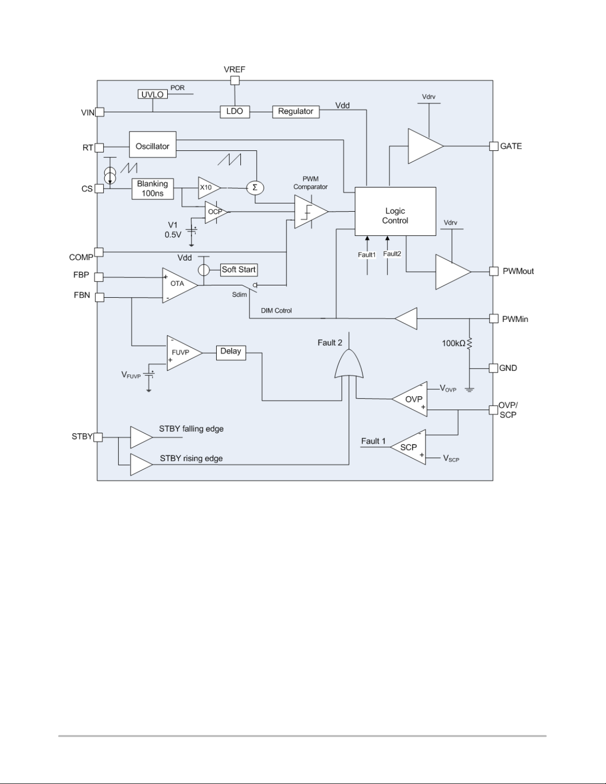
Figure 1. Block Diagram
http://onsemi.com
2
Page 3
NCS29001
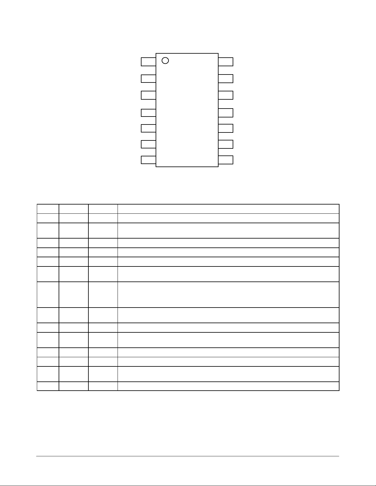
PINOUT ASSIGNMENT
VIN
Vref
GND
PWMin
RT
FBP
STBY
1
2
3
4
5
6 9
7 8
NCS29001
GATE
14
13
CS
12
PGND
11
PMWout
10 FBN
COMP
OVP
Figure 2. NSC29001 Pinout
PIN DESCRIPTION
Pin # Symbol Type Description
1 VIN Input
2 VREF Output
3 GND Ground Analog ground.
4 PWMin Output PWM dimming control input.
5 RT Output The resistor connected between RT and GND sets the switching frequency
6 FBP Input The reference voltage for the feedback (FBN). Reference level can be adjusted from 0.5 V up to
7 STBY Input The converter enters in standby mode when STBY is floating or pulled high. When STBY goes
8 OVP Output This pin provides the overvoltage protection for the converter. When the voltage at this pin
9 COMP Power Loop compensation pin
10 FBN Input Feedback pin and LED cathode connection. External resistor from FBN to GND sets the LED
11 PWMout Output PWM dimming output driver.
12 PGND Ground Power ground.
13 CS Power This pin is used to sense the drain current of the external power MOSFET. It includes a built−in
14 GATE Output This pin is the output GATE driver for an external N−channel power MOSFET
VIN supply input. Small 1.0 mF low ESR bypass capacitor required from VIN to GND.
5 V / 10 mA reference voltage. Small 1.0 mF low ESR bypass capacitor required from VREF to
GND.
3.0 V using an external voltage divider.
from low to high the circuit will discharge the capacitors on the COMP pin and keep PWMout high
to discharge the output capacitor. STBY must remain high for 50 ms before the part enters
standby mode.
exceeds 1.2 V, the boost converter stops immediately and the device enters standby mode.
current.
blanking time.
http://onsemi.com
3
Page 4
NCS29001
ATTRIBUTES
Characteristics Values
ESD protection (all pins)
Human Body Model (HBM) (Note 1)
Machine Model (MM)
Moisture sensitivity (Note 2) Level 1
Flammability Rating Oxygen Index: 28 to 34 UL 94 V−0 @ 0.125 in
Meets or exceeds JEDEC Spec EIA/JESD78 IC Latch−up Test
1. Human Body Model (HBM), R = 1500 W, C = 100 pF.
2. For additional information, see Application Note AND8003/D.
ABSOLUTE MAXIMUM RATINGS
Rating V
V
IN
PWMin −0.3 5.5 V
STBY −0.3 5.5 V
FBP −0.3 5.5 V
FBN −0.3 5.5 V
OVP −0.3 5.5 V
CS −0.3 5.5 V
Stresses exceeding Maximum Ratings may damage the device. Maximum Ratings are stress ratings only. Functional operation above the
Recommended Operating Conditions is not implied. Extended exposure to stresses above the Recommended Operating Conditions may
affect device reliability.
2 kV
150 V
MIN
V
MAX
−0.3 30 V
Unit
OPERATING CONDITIONS (T
V
IN
= +25°C)
A
Rating
Min Typ Max Unit
8.5 12 18 V
VIL_PWMin: PWMin input low voltage 1 V
VIH_PWMin: PWMin input high voltage 2 V
FBP 0.5 3.0 V
VIL_STBY: STBY input low voltage 1 V
VIH_STBY: STBY input high voltage 2 V
RT clock frequency resistor (Note 3) 20 140
Fdim dimming frequency (5 V amplitude) 100 300 Hz
Ddim dimming duty−cycle 3 95 %
NOTE: With respect to the GND pin.
3. Choose RT to keep clock frequency between 100 kHz and 500 kHz.
THERMAL RATINGS
Parameter Symbol Rating Unit
Junction to ambient thermal impedance (Note 4)
Maximum Junction Temperature (Note 5) T
Operating Ambient Temperature T
Storage temperature T
R
q
JA
J
A
stg
4. Power dissipation must be considered to ensure maximum junction temperature (qJA) is not exceeded.
5. Thermal Pad attached to PCB, 0 lfm airflow, and 76 mm x 76 mm copper area.
150 °C/W
+150 °C
−40 to +85 °C
−65 to +150 °C
kW
http://onsemi.com
4
Page 5
NCS29001
ELECTRICAL SPECIFICATIONS V
Symbol
Parameter Condition Min Typ Max Unit
= 12 V, T
IN
= –40°C to 85°C; typical values are at 25°C
AMB
VIN (VIN Pin)
I
VIN
I
SHUTDOWN
Operating Supply Current VIN = 12 V; PWMin = 5 V; no load,
STBY = 5 V
Shutdown Mode Supply Current PWMin = GND
Ambient temperature 25°C
5 mA
12 uA
STBY = 5 V
UVLO Under Voltage Lockout
VIN Rising 7.5 8 8.5 V
Threshold
DUVLO
T
startup
UVLO Hysteresis 475 mV
Startup time Time from standby falling edge to
steady−state V
dimming pattern − (Note 6)
operation with 30%
boost
100 ms
VREF (VREF Pin)
VREF
Vref voltage
REF bypassed with a 1 mF capacitor to
4.95 5 5.05 V
GND
Line_Reg Line Regulation VIN = 8.5 V to 24 V at I_REF = 10 mA 0.08 0.20 %
Load_Reg Load Regulation 0 mA < I_REF < 10 mA at VIN = 12 V 0.6 mV/mA
ICC (Vref) Iref output current
VREF bypassed with a 1 mF capacitor
10 mA
to GND
GATE (GATE, RT Pins)
V
OH_GATE
I
SOURCE
I
SINK
T
RISE
T
FALL
R
OH
R
OL
D
LSS_MAX
F
OSC
±DF
V
RT
OSC
GATE output high voltage VIN = 12 V 7.5 10 15 V
GATE short circuit current 0.33 0.45 A
GATE sinking current 0.33 0.45 A
GATE output rise time Output voltage rise−time @ CL = 1 nF,
− 40 ns
10−90% of output signal (Note 6)
GATE output fall time Output voltage fall−time @ CL = 1 nF,
− 20 ns
90−10% of output signal (Note 6)
Source resistance 13
Sink resistance 6.0
Maximum Duty Cycle (Note 6) 93 95 %
Boost Switching Frequency
100 500 kHz
range
Frequency Accuracy −10 +10 %
RT pin output voltage 0.85 1 1.15 V
PWM DIMMING (PWMin, PWMout Pins)
V
OH_PWMout
DD_DIM
PWMout output high voltage VIN = 12 V 7.5 10 15 V
PWMout/PWMin Duty cycle
0.98 1 1.02 %
Tolerance
T
RISE
T
FALL
I
SOURCE
I
SINK
R
OH
R
OL
PWMout output rise time Output voltage rise−time @ CL = 1 nF,
− − 2 us
10−90% of output signal
PWMout output fall time Output voltage fall−time @ C
90−10% of output signal
= 1 nF,
L
− − 2 us
PWMout short circuit current 15 20 mA
PWMout sinking current 15 20 mA
Source resistance 270
Sink resistance 230
6. Guaranteed by characterization and design
W
W
W
W
http://onsemi.com
5
Page 6
NCS29001
ELECTRICAL SPECIFICATIONS V
= 12 V, T
IN
Symbol UnitMaxTypMinConditionParameter
CURRENT SENSE (CS Pin)
V
CS
Reference voltage threshold for
current clamp monitoring OCP
comparator
I
RAMP
Slope compensation ramp 130 A/s
PROTECTION (OVP, FBP, FBN Pins)
V
V
V
UVPfb
T
DT
OVP
SCP
SD
SD
Output Overvoltage Protection
on OVP pin
Short Circuit Protection on OVP
pin
Output Undervoltage Protection
on FBN
Thermal Shutdown (Note 6) 140 150 160 °C
TSD hytheresis (Note 6) 15 °C
STANDBY (STBY Pin)
T
STANDBY
Standby mode delay (Note 6) 50 ms
6. Guaranteed by characterization and design
= –40°C to 85°C; typical values are at 25°C
AMB
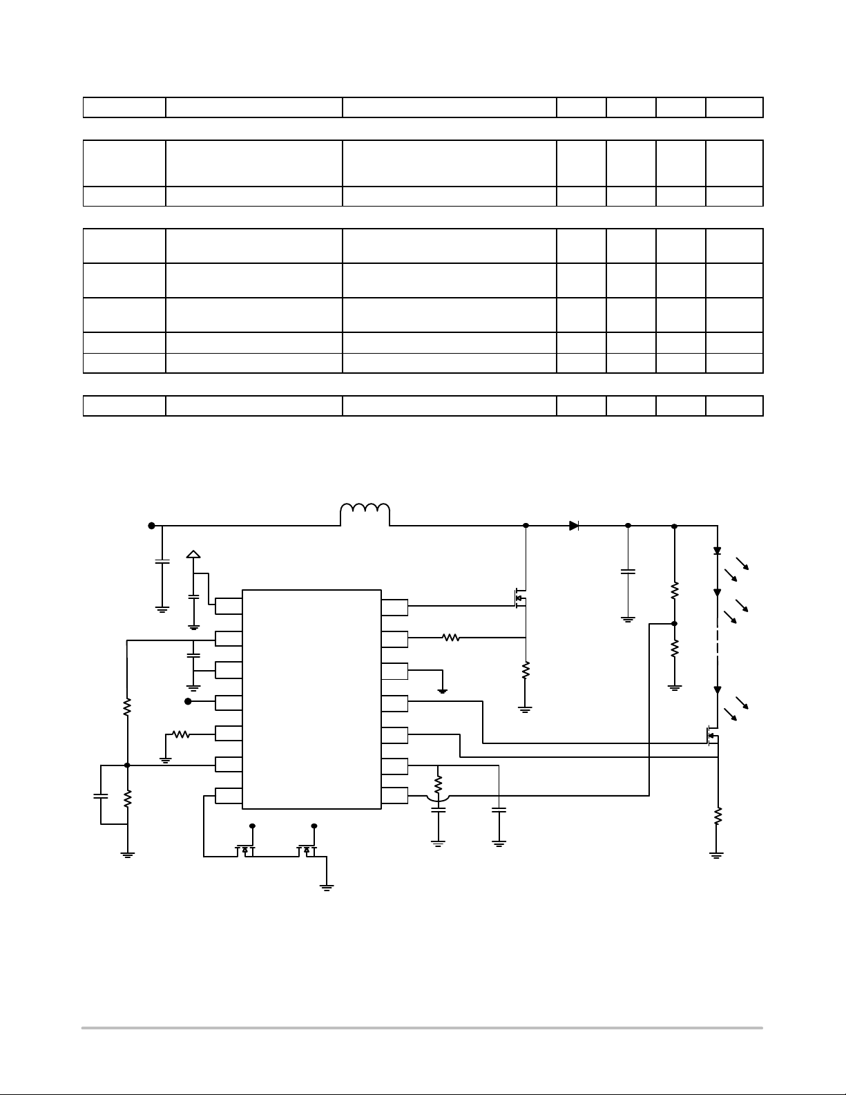
APPLICATION DIAGRAM
0.5 0.6 V
1.2 1.3 V
60 75 mV
60 75 mV
V
Rref1
Rref2
IN
VIN
Inductor
R
Q1
RCS
Q1
D1
C
OUT
R
R
OVP1
OVP2
Q2
L
VIN
IC
NCS29001
1
VIN
2
Vref
3
4
PWMin
5
T
RT
6 FBP COMP
7 8STBY OVP
Backlight O
Standby
PWMout
GATE
PGNDGND
FBN
CS
14
R
sc
13
12
11
10
9
R
comp
C
comp
C
comp2
Figure 3. Application Schematic
http://onsemi.com
6
Page 7

NCS29001
APPLICATION CONDITIONS
Symbol Parameter Condition Min Typ Max Unit
VIN
VIN
Dς
IC
Inductor
V
OUT
h
ΟΥΤ
Standby
VIN pin voltage 8.5 12 18 V
Inductor input voltage 8.5 80
Output voltage range V
VIN
Inductor
VIN
Inductor
VIN
Inductor
Peak efficiency VINIC = 12 V, V
VIN
= 12 V, V
IC
Output Voltage Accuracy including voltage ripple, from −40°C to 85°C,
/VIN
OUT
= 8.5 to 24 V | V
Inductor
= 24 to 50 V | V
= 50 to 80 V | V
= 130 V, I
OUT
= 240 V, I
OUT
VIN
= 8.5 V to 18 V
IC
Max = 5
= 50 to 80 V
OUT
= 80 to 130 V
OUT
= 130 to 240 V
OUT
= 200 mA
OUT
= 200 mA
OUT
50 240 V
95
95
−2 2 %
POWER UP SEQUENCE
VIN
%
UVLO
PWMin
Vcomp
PWMout
GATE
Figure 4. Soft Start Power Up from Standby
For the device to begin the soft start sequence the VIN pin voltage needs to be above the UVLO threshold and the OVP pin
voltage needs to be above the V
threshold. From standby mode soft start will begin when STBY pin goes low and PWMin
SCP
pin goes high and lasts for a fixed number of clock cycles. This ensures that smooth start up if the device is powered on from
standby with a PWM input.
http://onsemi.com
7
Page 8

Vout
Standby
VIN
Vin IC
PWMin
NCS29001
STANDBY ON AND OFF SEQUENCE
Discharging the
output capacitor
UVLO
Vfb & I(LED)
PWMout
GATE
Figure 5. Entering Standby Mode
The STBY pin contains an internal 5 MW pull−up resistor to VREF. This resistor limits current consumption when the device
is in standby mode and also ensures the device will remain in standby if the STBY pin is left floating.
When the STBY goes high the boost converter will stop switching and the PWMout pin will switch, or remain high for 50 ms.
This allows the output capacitor to discharge and the LED current to fall to zero. The device will be in a low power standby
mode and can begin soft start from the next enable sequence.
http://onsemi.com
8
Page 9

VCC > UVLO
POR
POR
NCS29001
STBY falling
edge?
N
STBY,10 uA
PWM Hi
Delay 100uS Max
during Soft start,
and reduced delay
PWMO high
FUVP?
Y
time for normal
operation
Control logic,
Y
Y
N
V1,V2,V4,Vref
Oscilator enabled
SCP&D1 Open?
N
Soft Start,
charging Rc,Cc
throug Iss
VFBN surpass
VFBP?
OTA take
control
PWM Dimming
OVP
N
Y, Fault1
Y
STBY rising
edge?
DRV grouded, PWMO
grounded
N
DRV goes low immediately,
PWMDout goes low
immediately
Y
Figure 6. Power Up State Machine
DRV goes low immediately,
PWMDout keeps high
discharging the output
Cc being discharged,
Delay 50 ms
STBY rising
edge?
0
capacitor,
000
>=1
Fault 2
‘
http://onsemi.com
9
Page 10

NCS29001
SOFT START WITH PWM INPUT
Figure 7 below shows an example of a soft start when the device is powered up from standby with a PWM input. The PWM
signal here is at 100 Hz with a duty cycle of 30%. In this case the LED reaches 100% of its programmed value in 100 ms. This
time can be decreased if the PWM signal runs at a higher duty cycle.
Soft start with PWM dimming active
100ms with 30% dimming duty cycle,
100Hz
PWMin and PWMout
Vfbp
Vfbn & LED
current
LED current reaches 100%
when Vfbn crosses Vfbp
Vcomp is kept during
dimming off
Back light LED brightness gradually
rise to the set value
Figure 7. Soft Start with PWM Input
GATE AND PWMOUT PIN DRIVER CIRCUIT
Since external transistors are required for the boost converter and PWM dimming functions, the device contains an internal
10 V regulator to drive the gate of these transistors. In the case of the PWM transistor this also functions as a level translator
for the PWMin input pin. When selecting external components it is important that the transistor has enough gate drive to ensure
low R
It should be noted that the internal 10 V regulator will start to drop when the VIN voltage is sufficiently low. When the V
for the expected current.
DS(on)
IN
voltage is 8.5 V the gate drivers will be limited to around 7.7 V.
http://onsemi.com
10
Page 11

NCS29001
VREF REFERENCE VOLTAGE
The device contains an accurate 5 V reference that can supply up to 10 mA and can be accessed through the VREF pin. It
can be used to program the LED feedback voltage by using a resistor divider on the FBP pin. This reference is only active when
STBY = low. When the device is in standby mode the VREF pin voltage will drop to 4.2 V typical with a minimum of 3.5 V.
The VREF will return to 5 V immediately when STBY is driven high.
MINIMUM ON & OFF TIME
If the steady state duty cycle and switching frequency combine to generate short Ton times (low VOUT/VIN converter ratio),
the converter will skip some cycles to regulate V
intrinsic loop propagation delay and the switching frequency will be limited by the minimum ON time and OFF time.
THE INDUCTOR SELECTION
For a given application, it is necessary to know the input voltage at the inductor (VIN
set by RFBN and the voltage on the FBP pin, and the switching frequency (F
below:
L
t
max
2 F
The minimal inductor value is determined with the desired peak current flowing through the inductor. Using the chosen
inductor value the steady state duty cycle and peak inductor current can be calculated:
which will increase output voltage ripple. The timing limit is set by the
OUT
), the output current (I
(eq. 1)
sw
1
I
OUT
INDUCTOR
). The inductor can be chosen using the formula
sw
2
V
IN
ǒ
Ǔ
ǒV
V
OUT
OUT
* V
Ǔ
IN
OUT
)
D +
Ǹ
2 L F
sw
I
OUT
V
ǒV
OUT
IN
* V
Ǔ
IN
(eq. 2)
And the inductor peak current is now:
THE CURRENT SENSE RESISTOR
I
peak
+
V
D
IN
L F
sw
+
Ǹ
2 I
OUT
(V
L F
OUT
sw
* VIN)
(eq. 3)
Set a current limit between 2 and 2.5 times the peak inductor current to account for inductor tolerance:
I
+ 2.5 I
limit
peak
(eq. 4)
The current limit reference fixed on the over-current protection comparator is VCS = 0.5 V and the resistance can be calculated
using following the equation:
V
RCS+
SLOPE COMPENSATION
2.5 I
CS
(eq. 5)
peak
After the current sense resistor is calculated additional calculations are needed for the external slope compensation ramp. Using
the R
value the typical slope of the compensation ramp can be calculated:
SENSE
Mramp +
1
2
R
SENSE
V
OUT
* V
L
IN
(eq. 6)
Using the typical value for , the external compensation resistor can be calculated as follows:
RSC+
RAMP
I
RAMP
(eq. 7)
M
The slope compensation ramp has an offset current, , which is used to calculate the peak ramp current and finally the adjusted
current sense resistor.
I
I
RAMP,peak
RCS+
V
CS
I
+ I
* RCS I
limit
OFF
) I
RAMP,peak
) D
RAMP
R
SW
RAMP,peak
(eq. 8)
(eq. 9)
http://onsemi.com
11
Page 12

NCS29001
OUTPUT CAPACITOR and OUTPUT VOLTAGE RIPPLE
Calculating the output voltage ripple will size the output capacitor value. The output voltage ripple equation below takes
into account the parasitic impedance (ESR) of this output capacitor:
I
ǒ1 * D
DV
COUT
+
DV
C
COUT
OUT
I
OUT
F
+
sw
OUT
C
OUT
ǒ1 *
F
Without taking into account the ESR, the output capacitor becomes:
I
C
OUT
u
DV
OUT
OUT
F
sw
If the ESR value of the selected output capacitor is high, the voltage ripple will increase. The error due to the ESR can be
estimated follow the equation below:
SIZING THE COMP PIN CAPACITOR
DV
OUTESR
+ ESR I
The transistor Q1 is turned ON (reset of the duty cycle) when the Vf of the output current amplifier reaches the control output
voltage V
In steady state, at DT
. The control voltage Vc is simply a reduced voltage out of the follower servicing the voltage on the COMP pin.
c
, the voltage at the current amplifier output is represented by the equation below:
sw
VC+ I
peak
Ǔ
2
sw
I
L F
peak
V
OUT
ǒ1 *
RCS G
) ESR I
sw
* V
IN
I
L F
peak
V
* V
OUT
peak
i
OUT
Ǔ
) ESR I
sw
Ǔ
IN
(eq. 13)
(eq. 14)
OUT
(eq. 10)
(eq. 11)
(eq. 12)
V
V
= COMP pin output voltage
comp
V
= Voltage Control of the transconductance amplifier
c
= voltage offset of the transconductance amplifier
V
os
i + C
dv
dt
Vf+
å C
+ VC) V
comp
V
D RCS G
IN
L F
i
EA
+
comp
V
sw
t
comp
OS
rise
i
+
i
EA
Vc) V
t
rise
os
(eq. 15)
(eq. 16)
(eq. 17)
iEA = 4 mA error amplifier output current capability
t
= soft start time
rise
V
= 0.9 V voltage offset due to the follower
os
So
i
t
EA
C
comp
C
comp
+ 0.7
VC) V
i
EA
L F
sw
rise
OS
30 ms
t
VIN D RCS G
L
) V
(eq. 18)
(eq. 19)
OS
During the soft start and with the dimming function activated, the COMP pin voltage is rising during 30 ms within the 100 ms
soft start time so V
holds for another during 70 ms afterwards. Attention needs to be brought to the DC voltage rating. As
comp
the capacitor value decreases and the DC voltage increases, the value chosen needs to be
http://onsemi.com
12
Page 13

NCS29001
SIZING THE R
Combining Equations 2 and 16 gives the following expression for I
RESISTOR for the LOOP STABILITY
comp
I
+
OUT
2 ǒV
OUT
V
f
* V
2
L F
IN
OUT
Ǔ ǒ
:
sw
RCS G
2
Ǔ
i
(eq. 20)
To obtain the small signal equation, partial derivates of the output current are calculated with respect to the control voltage Vc
and the output voltage V
OUT
.
V
C
* V
OUT
2
V
C
* V
L F
2
Ǔ
ǒRCS G
IN
L F
Ǔ ǒ
IN
sw
sw
RCS G
+
2
Ǔ
i
2
Ǔ
i
I
OUT
V
* V
OUT
IN
(eq. 21)
(eq. 22)
I
OUT
∂
+
V
∂
OUT
ǒ
I
OUT
∂
+
V
∂
OUT
2 ǒV
V
OUT
From the AC model below the control to output transfer function can be calculated:
Where
The dynamic resistance r
Z
(s) +
OUT
R1+
AC(LED)
Figure 8. Control to Output Transfer Function
I
OUT
V
ǒ
ǒ
OUT
H(s) +
ESR )
ESR )
1
+
(s)
(s)
H(s) + Z
1
sC
OUT
1
sC
OUT
2
V
ǒ
V
OUT
V
C
Ǔ
R
Ǔ
) R
Req+
OUT
V
(s)
(s)
OUT
eq
eq
* V
2
Fsw L
c
V
OUT
+
I
(s)
+ Req
R
R
ac
Rac R
2
Ǔ
ǒRcs G
IN
(s)
(s)
I
OUT
V
I
OUT
VC(s)
(s)
(s)
C
1 ) s ESR C
1 ) s C
1
1
is evaluated using the LED specification.
RAC+ R
sense
) r
AC(LED)
nb
i
LED
Ǔ
(s)
2
OUT
+
ǒ
ESR ) R
V
OUT
I
OUT
(eq. 23)
(eq. 24)
OUT
* V
(eq. 27)
Ǔ
eq
IN
(eq. 25)
(eq. 26)
http://onsemi.com
13
Page 14

NCS29001
Theory
The control to output transfer function is expressed following the formula below:
s
1 )
w
1 )
Ǔ ǒ
z
s
s
p
sw
RCS G
Ǔ
I
Where
Ho+
I
∂
∂
OUT
V
C
Req+
H(s) + H0
V
L F
C
ǒ
V
* V
OUT
IN
2
(eq. 28)
R
R
AC
RAC) R
1
1
(eq. 29)
Ho+
Ǹ
2 I
fp+
ǒ
OUT
V
OUT
2p
L F
Ǔ
* V
IN
ǒ
ESR ) R
sw
1
G
R
CS
1
Ǔ
C
eq
OUT
i
R
R
AC
RAC) R
1
1
(eq. 30)
(eq. 31)
There is also a right half plane zero:
fz+
2p ESR C
1
OUT
(eq. 32)
As the boost converter also operates in DCM, there is also a right half plane zero regulated to high frequency:
f
rhpz
+
sw
2p D
(eq. 33)
2 f
Type II compensation is used to compensate the two dominant poles fp of the control to output transfer function.
The compensator zero has to be placer at the f
fp+
2p (ESR ) Req) C
frequency of the transfer function.
p
R
1
comp
(ESR ) R
+
OUT
+ fz+
) C
eq
C
comp
2p R
OUT
comp
1
C
comp
(eq. 35)
(eq. 34)
The dominant pole is expressed following the equation:
fp1+
2p REA C
1
comp
(eq. 36)
−
COMP
9
+
gm
Type II
Rcomp
Ccomp
Compensation
Figure 9. Slope Compensation Network
The natural second pole is expressed following the equation:
fp2+
2p R
The zero is expressed following the equation:
fz+
2p R
http://onsemi.com
C
1
comp
1
comp
14
equivalent
C
bw =
pad+Comp2
C
bw
C
comp
Cpad
With
Ccomp2
Cpad=10pF
(eq. 37)
(eq. 38)
Page 15

NCS29001
OSCILLATOR FREQUENCY SETTING
The simplified equation to set the switching frequency using resistor RT:
13750
fsw+
) 5
R
T
(eq. 39)
Where:
is expressed in kW.
R
T
f
us expressed in kHz
sw
FBP OPTIONS
The FBP pin is used to program the feedback voltage that sets the LED current. Typically a resistor divider is used from VREF
to set the voltage between 0.5 V and 3.0 V. Additionally, to save component costs, the feedback voltage can be programmed
with internal 0.8 V (±1.5%) by tying the FBP pin to ground.
FAULT DETECTION:
• Overvoltage Protection: A resistor divider from VOUT can be used to set the overvoltage protection on the OVP pin.
When the OVP pin rises above 1.2 V the converter will shut off immediately and PWMout will be held high for 50 ms
to discharge the output capacitor. After this time the device will enter standby mode requires a high to low transition on
the STBY pin to restart.
• Short Circuit Protection: A resistor divider from VOUT can be used to set the short circuit protection on the OVP pin.
When the OVP pin drops below 75 mV the converter will shut off immediately and enter standby mode. A high to low
transition on the STBY pin is required to restart the device.
• Under Voltage Lockout (UVLO): The converter will immediately shut off and enter standby when the VIN pin voltage
drops below 7.5 V. When the UVLO condition is cleared, a high to low transition on the STBY pin is required to restart
the device.
• Temperature Shutdown: When the internal die temperature reaches 150°C, the device will behave the same as in the
overvoltage condition.
Layout Guidance
In switching converters it is important to use wide, short traces for components in the main switching path. Resistor RCS,
which is in the main switching path through transistor Q1, should be connected to power ground (PGND). Compensation
network components, resistor dividers, and bypass capacitors should be referenced to quiet ground (GND). Bypass capacitors
should be connected as close to the IC as possible.
ORDERING INFORMATION
Device Package Shipping
NCS29001DR2G SOIC−14
(Pb−Free)
†For information on tape and reel specifications, including part orientation and tape sizes, please refer to our Tape and Reel Packaging
Specifications Brochure, BRD8011/D.
3000 / Tape & Reel
†
http://onsemi.com
15
Page 16

MECHANICAL CASE OUTLINE
PACKAGE DIMENSIONS
14
1
SCALE 1:1
SOIC−14 NB
CASE 751A−03
ISSUE L
DATE 03 FEB 2016
14
H
M
0.25 B
0.10
14X
0.58
D
M
13X
e
SOLDERING FOOTPRINT*
6.50
1
A
B
8
E
71
b
S
M
0.25 B
A
C
A
A1
SEATING
C
PLANE
1.18
14X
S
1.27
PITCH
DETAIL A
h
X 45
_
M
NOTES:
1. DIMENSIONING AND TOLERANCING PER
ASME Y14.5M, 1994.
2. CONTROLLING DIMENSION: MILLIMETERS.
3. DIMENSION b DOES NOT INCLUDE DAMBAR
A3
L
DETAIL A
PROTRUSION. ALLOWABLE PROTRUSION
SHALL BE 0.13 TOTAL IN EXCESS OF AT
MAXIMUM MATERIAL CONDITION.
4. DIMENSIONS D AND E DO NOT INCLUDE
MOLD PROTRUSIONS.
5. MAXIMUM MOLD PROTRUSION 0.15 PER
SIDE.
DIM MIN MAX MIN MAX
A 1.35 1.75 0.054 0.068
A1 0.10 0.25 0.004 0.010
A3 0.19 0.25 0.008 0.010
b 0.35 0.49 0.014 0.019
D 8.55 8.75 0.337 0.344
E 3.80 4.00 0.150 0.157
e 1.27 BSC 0.050 BSC
H 5.80 6.20 0.228 0.244
h 0.25 0.50 0.010 0.019
L 0.40 1.25 0.016 0.049
M 0 7 0 7
__ __
INCHESMILLIMETERS
GENERIC
MARKING DIAGRAM*
14
XXXXXXXXXG
AWLYWW
1
XXXXX = Specific Device Code
A = Assembly Location
WL = Wafer Lot
Y = Year
WW = Work Week
G = Pb−Free Package
*This information is generic. Please refer to
device data sheet for actual part marking.
Pb−Free indicator, “G” or microdot “ G”,
may or may not be present.
DIMENSIONS: MILLIMETERS
*For additional information on our Pb−Free strategy and soldering
details, please download the ON Semiconductor Soldering and
Mounting Techniques Reference Manual, SOLDERRM/D.
STYLES ON PAGE 2
DOCUMENT NUMBER:
DESCRIPTION:
ON Semiconductor and are trademarks of Semiconductor Components Industries, LLC dba ON Semiconductor or its subsidiaries in the United States and/or other countries.
ON Semiconductor reserves the right to make changes without further notice to any products herein. ON Semiconductor makes no warranty, representation or guarantee regarding
the suitability of its products for any particular purpose, nor does ON Semiconductor assume any liability arising out of the application or use of any product or circuit, and specifically
disclaims any and all liability, including without limitation special, consequential or incidental damages. ON Semiconductor does not convey any license under its patent rights nor the
rights of others.
© Semiconductor Components Industries, LLC, 2019
98ASB42565B
SOIC−14 NB
Electronic versions are uncontrolled except when accessed directly from the Document Repository.
Printed versions are uncontrolled except when stamped “CONTROLLED COPY” in red.
PAGE 1 OF 2
www.onsemi.com
Page 17

SOIC−14
CASE 751A−03
ISSUE L
DATE 03 FEB 2016
STYLE 1:
PIN 1. COMMON CATHODE
2. ANODE/CATHODE
3. ANODE/CATHODE
4. NO CONNECTION
5. ANODE/CATHODE
6. NO CONNECTION
7. ANODE/CATHODE
8. ANODE/CATHODE
9. ANODE/CATHODE
10. NO CONNECTION
11. ANODE/CATHODE
12. ANODE/CATHODE
13. NO CONNECTION
14. COMMON ANODE
STYLE 5:
PIN 1. COMMON CATHODE
2. ANODE/CATHODE
3. ANODE/CATHODE
4. ANODE/CATHODE
5. ANODE/CATHODE
6. NO CONNECTION
7. COMMON ANODE
8. COMMON CATHODE
9. ANODE/CATHODE
10. ANODE/CATHODE
11. ANODE/CATHODE
12. ANODE/CATHODE
13. NO CONNECTION
14. COMMON ANODE
STYLE 2:
CANCELLED
STYLE 6:
PIN 1. CATHODE
2. CATHODE
3. CATHODE
4. CATHODE
5. CATHODE
6. CATHODE
7. CATHODE
8. ANODE
9. ANODE
10. ANODE
11. ANODE
12. ANODE
13. ANODE
14. ANODE
STYLE 3:
PIN 1. NO CONNECTION
2. ANODE
3. ANODE
4. NO CONNECTION
5. ANODE
6. NO CONNECTION
7. ANODE
8. ANODE
9. ANODE
10. NO CONNECTION
11. ANODE
12. ANODE
13. NO CONNECTION
14. COMMON CATHODE
STYLE 7:
PIN 1. ANODE/CATHODE
2. COMMON ANODE
3. COMMON CATHODE
4. ANODE/CATHODE
5. ANODE/CATHODE
6. ANODE/CATHODE
7. ANODE/CATHODE
8. ANODE/CATHODE
9. ANODE/CATHODE
10. ANODE/CATHODE
11. COMMON CATHODE
12. COMMON ANODE
13. ANODE/CATHODE
14. ANODE/CATHODE
STYLE 4:
PIN 1. NO CONNECTION
2. CATHODE
3. CATHODE
4. NO CONNECTION
5. CATHODE
6. NO CONNECTION
7. CATHODE
8. CATHODE
9. CATHODE
10. NO CONNECTION
11. CATHODE
12. CATHODE
13. NO CONNECTION
14. COMMON ANODE
STYLE 8:
PIN 1. COMMON CATHODE
2. ANODE/CATHODE
3. ANODE/CATHODE
4. NO CONNECTION
5. ANODE/CATHODE
6. ANODE/CATHODE
7. COMMON ANODE
8. COMMON ANODE
9. ANODE/CATHODE
10. ANODE/CATHODE
11. NO CONNECTION
12. ANODE/CATHODE
13. ANODE/CATHODE
14. COMMON CATHODE
DOCUMENT NUMBER:
DESCRIPTION:
ON Semiconductor and are trademarks of Semiconductor Components Industries, LLC dba ON Semiconductor or its subsidiaries in the United States and/or other countries.
ON Semiconductor reserves the right to make changes without further notice to any products herein. ON Semiconductor makes no warranty, representation or guarantee regarding
the suitability of its products for any particular purpose, nor does ON Semiconductor assume any liability arising out of the application or use of any product or circuit, and specifically
disclaims any and all liability, including without limitation special, consequential or incidental damages. ON Semiconductor does not convey any license under its patent rights nor the
rights of others.
© Semiconductor Components Industries, LLC, 2019
98ASB42565B
SOIC−14 NB
Electronic versions are uncontrolled except when accessed directly from the Document Repository.
Printed versions are uncontrolled except when stamped “CONTROLLED COPY” in red.
PAGE 2 OF 2
www.onsemi.com
Page 18

ON Semiconductor and are trademarks of Semiconductor Components Industries, LLC dba ON Semiconductor or its subsidiaries in the United States and/or other countries.
ON Semiconductor owns the rights to a number of patents, trademarks, copyrights, trade secrets, and other intellectual property. A listing of ON Semiconductor’s product/patent
coverage may be accessed at www.onsemi.com/site/pdf/Patent−Marking.pdf
ON Semiconductor makes no warranty, representation or guarantee regarding the suitability of its products for any particular purpose, nor does ON Semiconductor assume any liability
arising out of the application or use of any product or circuit, and specifically disclaims any and all liability, including without limitation special, consequential or incidental damages.
Buyer is responsible for its products and applications using ON Semiconductor products, including compliance with all laws, regulations and safety requirements or standards,
regardless of any support or applications information provided by ON Semiconductor. “Typical” parameters which may be provided in ON Semiconductor data sheets and/or
specifications can and do vary in different applications and actual performance may vary over time. All operating parameters, including “Typicals” must be validated for each customer
application by customer’s technical experts. ON Semiconductor does not convey any license under its patent rights nor the rights of others. ON Semiconductor products are not
designed, intended, or authorized for use as a critical component in life support systems or any FDA Class 3 medical devices or medical devices with a same or similar classification
in a foreign jurisdiction or any devices intended for implantation in the human body. Should Buyer purchase or use ON Semiconductor products for any such unintended or unauthorized
application, Buyer shall indemnify and hold ON Semiconductor and its officers, employees, subsidiaries, affiliates, and distributors harmless against all claims, costs, damages, and
expenses, and reasonable attorney fees arising out of, directly or indirectly, any claim of personal injury or death associated with such unintended or unauthorized use, even if such
claim alleges that ON Semiconductor was negligent regarding the design or manufacture of the part. ON Semiconductor is an Equal Opportunity/Affirmative Action Employer. This
literature is subject to all applicable copyright laws and is not for resale in any manner.
. ON Semiconductor reserves the right to make changes without further notice to any products herein.
PUBLICATION ORDERING INFORMATION
LITERATURE FULFILLMENT:
Email Requests to: orderlit@onsemi.com
ON Semiconductor Website: www.onsemi.com
TECHNICAL SUPPORT
North American Technical Support:
Voice Mail: 1 800−282−9855 Toll Free USA/Canada
Phone: 011 421 33 790 2910
Europe, Middle East and Africa Technical Support:
Phone: 00421 33 790 2910
For additional information, please contact your local Sales Representative
◊
www.onsemi.com
1
 Loading...