

Page 1
45 mV Offset, 0.4 mV/5C,
Zero-Drift Operational
Amplifier
NCS21871, NCV21871,
NCS21872, NCV21872,
NCS21874, NCV21874
The NCS21871, NCS21872 and NCS21874 family of zero−drift op
amps feature offset voltage as low as 45 mV over the 1.8 V to 5.5 V
supply voltage range. The zero−drift architecture reduces the offset
drift to as low as 0.4 mV/°C and enables high precision measurements
over both time and temperature. This family has low power
consumption over a wide dynamic range and is available in space
saving packages. These features make it well suited for signal
conditioning circuits in portable, industrial, automotive, medical and
consumer markets.
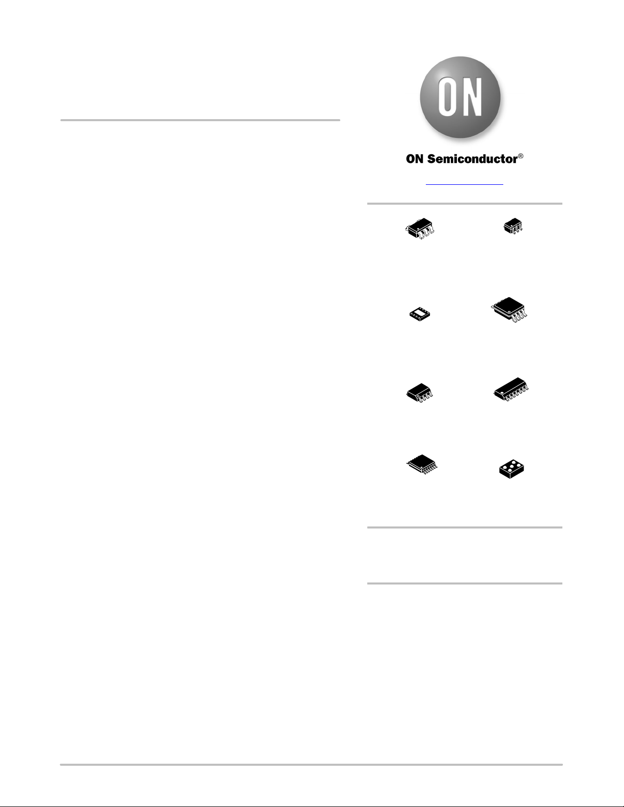
www.onsemi.com
5
1
SOT23−5
SN SUFFIX
CASE 483
5
1
SC70−5
SQ SUFFIX
CASE 419A
Features
• Gain−Bandwidth Product: 270 kHz to 350 kHz
• Low Supply Current: 17 mA (typ at 3.3 V)
• Low Offset Voltage: 45 mV max
• Low Offset Drift: 0.4 mV/°C max
• Wide Supply Range: 1.8 V to 5.5 V
• Wide Temperature Range: −40°C to +125°C
• Rail−to−Rail Input and Output
• Available in Single, Dual and Quad Packages
• NCV Prefix for Automotive and Other Applications Requiring
Unique Site and Control Change Requirements; AEC−Q100
Qualified and PPAP Capable
Applications
• Automotive
• Battery Powered/ Portable Application
• Sensor Signal Conditioning
• Low Voltage Current Sensing
• Filter Circuits
• Bridge Circuits
• Medical Instrumentation
1
UDFN8
MU SUFFIX
CASE 517AW
8
1
SOIC−8
D SUFFIX
CASE 751
14
1
TSSOP−14 WB
DT SUFFIX
CASE 948G
DEVICE MARKING INFORMATION
See general marking information in the device marking
section on page 2 of this data sheet.
ORDERING INFORMATION
See detailed ordering and shipping information on page 3 of
this data sheet.
MSOP−8
DM SUFFIX
CASE 846A−02
14
1
SOIC−14
D SUFFIX
CASE 751A
ECP5
FCT SUFFIX
CASE 971BE
© Semiconductor Components Industries, LLC, 2019
April, 2021 − Rev. 2
1 Publication Order Number:
NCS21871/D
Page 2
NCS21871, NCV21871, NCS21872, NCV21872, NCS21874, NCV21874
DEVICE MARKING INFORMATION
Single Channel Configuration
NCS21871, NCV21871
72
YM
1
UDFN8, 2x2, 0.5P
CASE 517AW
7AAYWG
G
TSOP−5/SOT23−5
CASE 483
14
N874G
AWLYWW
1
SOIC−14
CASE 751A
7CMG
G
SC70−5
CASE 419A
Dual Channel Configuration
NCS21872, NCV21872
8
2187
AYW G
G
1
Micro8/MSOP8
CASE 846A−02
Quad Channel Configuration
NCS21874, NCV21874
XXX
AYW
G
ECP5
CASE 971BE
14
N874
ALYWG
G
1
TSSOP−14 WB
CASE 948G
8
21872
ALYW
1
SOIC−8
CASE 751
G
N874 = Specific Device Code
A = Assembly Location
Y = Year
W = Work Week
M = Date Code
G or G = Pb−Free Package
N874 = Specific Device Code
A = Assembly Location
L = Wafer Lot
Y = Year
W = Work Week
G = Pb−Free Package
(Note: Microdot may be in either location)
www.onsemi.com
2
Page 3
NCS21871, NCV21871, NCS21872, NCV21872, NCS21874, NCV21874
PIN CONNECTIONS
Single Channel Configuration
NCS21871, NCV21871
OUT
VSS
1
VDD
5
2
IN+
34
SOT23−5 / TSOP−5
Dual Channel Configuration
NCS21872, NCV21872
OUT 1
*The exposed pad of the UDFN8 package
can be floated or connected to VSS.
1
−
2
IN− 1
+
3
IN+ 1
VSS
4
UDFN8* / Micro8 / SOIC−8
IN−
1
IN+
2
VSS
34
IN−
SC70−5 / SC−88−5 / SOT−353−5
8
VDD
7
OUT 2
6
IN− 2
−
+
IN+ 2
5
5
OUT 1
IN− 1
IN+ 1
VDD
IN+ 2
IN− 2
OUT 2
VDD
OUT
VSS
OUT
Quad Channel Configuration
NCS21874, NCV21874
VDD
1
2
−
+
3
4
5
+
−
6
7
SOIC−14, TSSOP−14
C3 C1
B2
A3 A1
ECP5 (Top View)
14
OUT 4
IN− 4
13
−
+
+
−
12
11
10
9
8
IN+ 4
VSS
IN+ 3
IN− 3
OUT 3
IN−
IN+
ORDERING INFORMATION
Temperature Channels Package Device Part Number Shipping
COMMERCIAL AND INDUSTRIAL
−40°C to 125°C
AUTOMOTIVE
−40°C to 125°C
†For information on tape and reel specifications, including part orientation and tape sizes, please refer to our Tape and Reel Packaging
Specifications Brochure, BRD8011/D.
*In Development. Contact local sales office for more information.
Single
Dual
Quad
Single
Dual
Quad
SOT23*5 / TSOP*5 NCS21871SN2T1G
SC70*5 / SC*88*5 /
SOT*353*5
ECP5 NCS21871FCTTAG*
MICRO*8 NCS21872DMR2G 4000 / Tape & Reel
SOIC−8 NCS21872DR2G
UDFN−8 NCS21872MUTBG*
SOIC−14 NCS21874DR2G
TSSOP−14 NCS21874DTBR2G
SOT23*5 / TSOP*5 NCV21871SN2T1G
SC70*5 / SC*88*5 /
SOT*353*5
MICRO*8 NCV21872DMR2G 4000 / Tape & Reel
SOIC−8 NCV21872DR2G 3000 / Tape & Reel
SOIC−14 NCV21874DR2G
TSSOP−14 NCV21874DTBR2G
NCS21871SQ3T2G
NCV21871SQ3T2G
3000 / Tape & Reel
3000 / Tape & Reel
2500 / Tape & Reel
3000 / Tape & Reel
2500 / Tape & Reel
†
www.onsemi.com
3
Page 4
NCS21871, NCV21871, NCS21872, NCV21872, NCS21874, NCV21874
ABSOLUTE MAXIMUM RATINGS
Over operating free−air temperature, unless otherwise stated.
Parameter Rating Unit
Supply Voltage 6 V
INPUT AND OUTPUT PINS
Input Voltage (Note 1)
Input Current (Note 1) ±10 mA
Output Short Circuit Current (Note 2) Continuous
TEMPERATURE
Operating Temperature Range
Storage Temperature Range −65 to +150 °C
Junction Temperature +150 °C
ESD RATINGS (Note 3)
Human Body Model (HBM)
Charged Device Model (CDM) ±2000 V
OTHER RATINGS
Latch−up Current (Note 4)
MSL Level 1
Stresses exceeding those listed in the Maximum Ratings table may damage the device. If any of these limits are exceeded, device functionality
should not be assumed, damage may occur and reliability may be affected.
1. Input terminals are diode−clamped to the power−supply rails. Input signals that can swing more than 0.3 V beyond the supply rails should
be current limited to 10 mA or less
2. Short−circuit to ground.
3. This device series incorporates ESD protection and is tested by the following methods:
ESD Human Body Model tested per JEDEC standard JS−001 (AEC−Q100−002)
ESD Charged Device Model tested per JEDEC standard JESD22−C101 (AEC−Q100−011)
4. Latch−up Current tested per JEDEC standard: JESD78.
(VSS) − 0.3 to (VDD) + 0.3 V
−40 to +125 °C
±4000 V
100 mA
THERMAL INFORMATION (Note 5)
Parameter
Thermal Resistance,
Junction to Ambient
5. As mounted on an 80x80x1.5 mm FR4 PCB with 650 mm2 and 2 oz (0.07 mm) thick copper heat spreader. Following JEDEC JESD/EIA 51.1,
51.2, 51.3 test guidelines
Symbol Package Value Unit
q
JA
SOT23−5 / TSOP5 290
SC70−5 / SC−88−5 / SOT−353−5 290
ECP5 157
Micro8 / MSOP8 298
SOIC−8 250
UDFN8 228
SOIC−14 216
TSSOP−14 155
°C/W
RECOMMENDED OPERATING CONDITIONS
Parameter Symbol Range Unit
Supply Voltage (VDD − VSS) V
Specified Operating Temperature Range T
Input Common Mode Voltage Range V
Functional operation above the stresses listed in the Recommended Operating Ranges is not implied. Extended exposure to stresses beyond
the Recommended Operating Ranges limits may affect device reliability.
S
A
CM
1.8 to 5.5 V
−40 to 125 °C
VSS−0.1 to VDD+0.1 V
www.onsemi.com
4
Page 5
NCS21871, NCV21871, NCS21872, NCV21872, NCS21874, NCV21874
ELECTRICAL CHARACTERISTICS: V
= +25°C, RL = 10 kW connected to midsupply, VCM = V
At T
A
Boldface limits apply over the specified operating temperature range, guaranteed by characterization and/or design.
Parameter
= 1.8 V to 5.5 V
S
= midsupply, unless otherwise noted.
OUT
Symbol Conditions Min Typ Max Unit
INPUT CHARACTERISTICS
Offset Voltage
Offset Voltage Drift vs Temp
Offset Voltage Drift vs Supply
V
OS
DVOS/DT
DVOS/DV
S
VS = +5 V 6 45
VS = 5 V 0.1 0.4
mV/°C
TA = +25°C 0.4 8 mV/V
Full temperature range 12.6
Input Bias Current
(Note 6)
Input Offset Current
(Note 6)
Common Mode Rejection Ratio
(Note 7)
I
IB
I
OS
CMRR
TA = +25°C ±60 ±400
Full temperature range +400
TA = +25°C ±50 ±800 pA
VS = 1.8 V 111
VS = 3.3 V 11 8
VS = 5.0 V 102 123
VS = 5.5 V 127
Input Capacitance C
IN
Differential 4.1
Common Mode 7.9
OUTPUT CHARACTERISTICS
Open Loop Voltage Gain
(Note 6)
Open Loop Output Impedance Z
Output Voltage High,
Referenced to V
DD
Output Voltage Low,
Referenced to V
SS
A
VOL
out−OL
V
OH
V
OL
I
O
VSS + 100 mV < VO < VDD − 100 mV 106 145 dB
See Figure 18
TA = +25°C 10 80
mV
Full temperature range 80
TA = +25°C 10 80
mV
Full temperature range 80
Sinking Current 11
mA
Sourcing Current 5.0
Capacitive Load Drive C
L
See Figure 14
NOISE PERFORMANCE
Voltage Noise Density
Voltage Noise e
e
N
P−P
fIN = 1 kHz 62 nV / √Hz
fIN = 0.1 Hz to 10 Hz 1.1 mV
fIN = 0.01 Hz to 1 Hz 0.5
Current Noise Density i
N
fIN = 10 Hz 350 fA / √Hz
Channel Separation NCS21872, NCS21874 135 dB
DYNAMIC PERFORMANCE
Gain Bandwidth Product
GBWP CL = 100 pF
NCS21871, NCS21874 350
kHz
NCS21872 270
Gain Margin A
Phase Margin
f
Slew Rate SR
M
M
CL = 100 pF 18 dB
CL = 100 pF 55 °
G = 1, VDD = 5.5 V 0.1 V/ms
G = 1, VDD = 1.8 V 0.05
6. Guaranteed by characterization and/or design
7. Specified over the full common mode range: V
8. No load, per channel
− 0.1 < VCM < VDD + 0.1
SS
mV
pA
dB
pF
W
PP
www.onsemi.com
5
Page 6
NCS21871, NCV21871, NCS21872, NCV21872, NCS21874, NCV21874
ELECTRICAL CHARACTERISTICS: V
= +25°C, RL = 10 kW connected to midsupply, VCM = V
At T
A
Boldface limits apply over the specified operating temperature range, guaranteed by characterization and/or design.
= 1.8 V to 5.5 V
S
= midsupply, unless otherwise noted.
OUT
Parameter UnitMaxTypMinConditionsSymbol
POWER SUPPLY
Power Supply Rejection Ratio
PSRR
TA = +25°C 106 130
dB
Full temperature range 98
Turn−on Time t
Quiescent Current
(Note 8)
ON
I
Q
VS = 5 V 100
1.8 V ≤ VS ≤ 3.3 V
3.3 V < VS ≤ 5.5 V
ms
20 40 mA
40
28 45
45
6. Guaranteed by characterization and/or design
7. Specified over the full common mode range: V
8. No load, per channel
− 0.1 < VCM < VDD + 0.1
SS
Product parametric performance is indicated in the Electrical Characteristics for the listed test conditions, unless otherwise noted. Product
performance may not be indicated by the Electrical Characteristics if operated under different conditions.
www.onsemi.com
6
Page 7
NCS21871, NCV21871, NCS21872, NCV21872, NCS21874, NCV21874
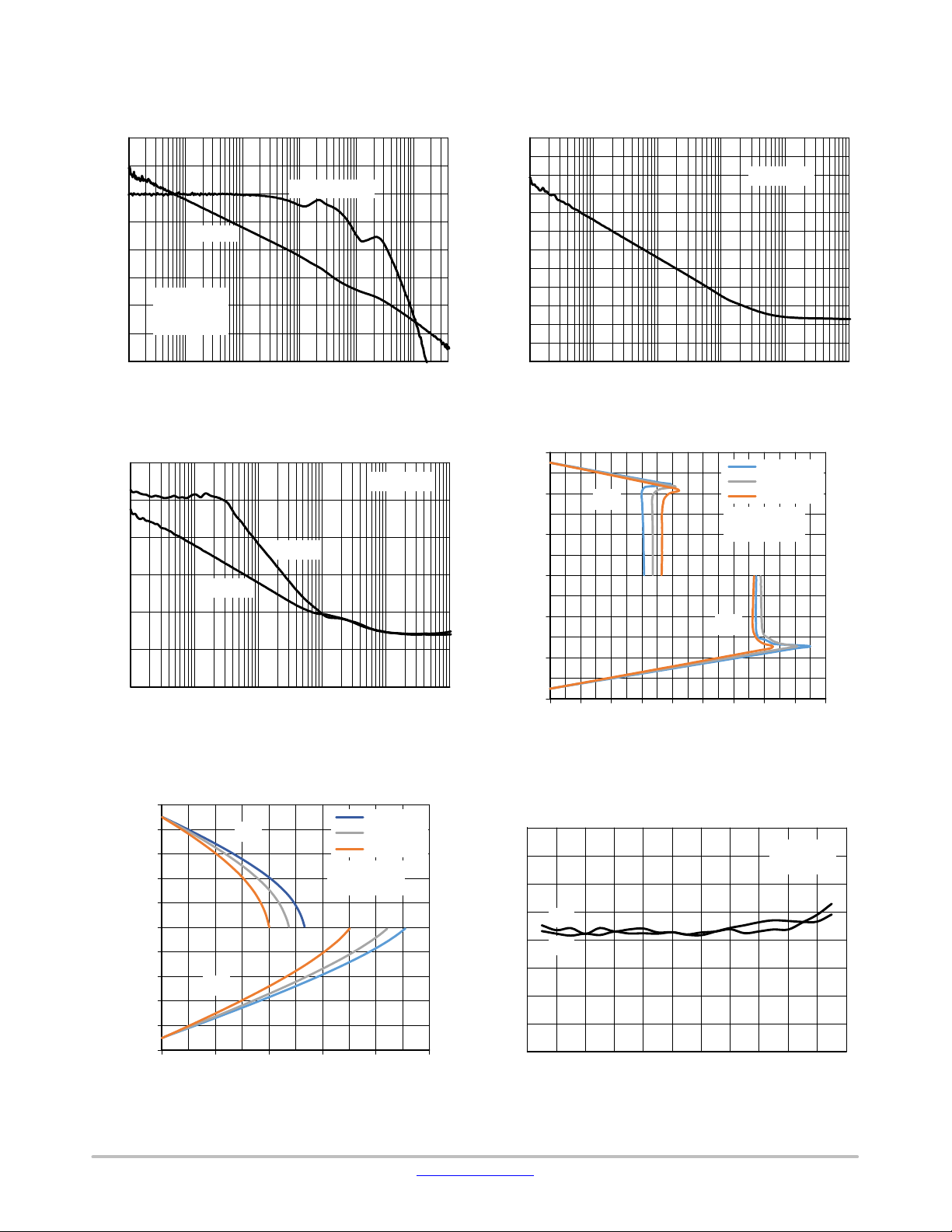
TYPICAL CHARACTERISTICS
120
100
80
60
40
GAIN (dB)
20
0
−20
−40
Figure 1. Open Loop Gain and Phase Margin
120
100
80
60
PSRR (dB)
40
20
Gain
CL = 100 pF
R
= 10 kW
L
T
= 25°C
A
−PSRR
PHASE MARGIN (°)
120
110
100
90
80
70
60
50
CMRR (dB)
40
30
20
10
0
120
105
Phase Margin
FREQUENCY (Hz) FREQUENCY (Hz)
90
75
60
45
30
15
0
1M100k10k1k10010
Figure 2. CMRR vs. Frequency
vs. Frequency
3
TA = 25°C
+PSRR
2
1
0
−1
OUTPUT VOLTAGE (V)
−2
V
OH
VDD = 2.75 V
VSS = −2.75 V
V
OL
TA = 25°C
1M100k10k1k10010
TA = −40 °C
TA = 25 °C
TA = 125 °C
0
0.8
0.6
0.4
0.2
−0.2
−0.4
OUTPUT VOLTAGE (V)
−0.6
−0.8
100k10k1k10010
FREQUENCY (Hz)
Figure 3. PSRR vs. Frequency
1
V
OH
0
V
OL
−1
0246810
OUTPUT CURRENT (mA)
TA = −40 °C
TA = 25 °C
TA = 125 °C
VDD = 0.9 V
VSS = −0.9 V
Figure 5. Output Voltage Swing vs. Output
Current at V
= 1.8 V
S
1M
−3
0 2 4 6 8 1012141618
OUTPUT CURRENT (mA)
Figure 4. Output Voltage Swing vs. Output
Current at V
200
150
100
50
I
IB+
0
I
IB−
−50
−100
INPUT BIAS CURRENT (pA)
−150
−200
0 0.6 1.0 1.6 2.0
COMMON MODE VOLTAGE (V)
Figure 6. Input Bias Current vs. Common
= 5.5 V
S
Mode Voltage
TA = 25°C
= 1.8 V
V
S
1.81.41.20.80.40.2−0.2
www.onsemi.com
7
Page 8

NCS21871, NCV21871, NCS21872, NCV21872, NCS21874, NCV21874
TYPICAL CHARACTERISTICS
200
150
100
50
0
−50
−100
INPUT BIAS CURRENT (pA)
−150
−200
TEMPERATURE (°C)
Figure 7. Input Bias Current vs. Temperature
4
3
2
1
0
INPUT (V)
−1
−2
−3
−4
VS = 5.0 V
A
V
R
L
Input
Output
= +1
= 10 kW
30
VS = 5.5 V
25
VS = 5.0 V
I
IB+
I
IB−
TA = 25°C
= 5 V
V
S
20
15
(mA)
Q
I
VS = 3.3 V
VS = 1.8 V
10
5
Per Channel
0
100806040200−20−40
100806040200−20−40
TEMPERATURE (°C)
Figure 8. Quiescent Current vs. Temperature
5
4
3
2
1
0
−1
−2
−3
0.20
0.15
0.10
0.05
0
OUTPUT (V)
−0.05
INPUT AND OUTPUT (V)
−0.10
−0.15
Input
Output
VS = 5.0 V
= −1
A
V
R
= 10 kW
L
1.0
0.5
0
−0.5
−1.0
−1.5
−2.0
−2.5
−3.0
INPUT (V)
TIME (50 ms/div)
Figure 9. Large Signal Step Response
Input
VS = 5.0 V
= −10
A
V
R
= 10 kW
Output
TIME (50 ms/div)
L
OUTPUT (V)
Figure 11. Positive Overvoltage Recovery
3.0
2.5
2.0
1.5
1.0
0.5
0
−0.5
−1.0
2.5
2.0
1.5
1.0
0.5
0
−0.5
−1.0
INPUT (V)
TIME (5 ms/div)
Figure 10. Small Signal Step Response
Output
VS = 5.0 V
= −10
A
V
R
= 10 kW
L
Input
OUTPUT (V)
TIME (50 ms/div)
Figure 12. Negative Overvoltage Recovery
1.03.0
0.5
0
−0.5
−1.0
−1.5
−2.0
−2.5
−3.0
www.onsemi.com
8
Page 9

NCS21871, NCV21871, NCS21872, NCV21872, NCS21874, NCV21874
√
TYPICAL CHARACTERISTICS
500
400
300
200
SETTLING TIME (ms)
100
2000
1500
1000
0
500
TA = 25°C
R
= 10 kW
L
GAIN (V/V)
Figure 13. Setting Time to 0.1% vs.
Closed−Loop Gain
0
VCM = VS/2
R
= 10 kW
L
T
= 25°C
A
65
60
55
50
45
40
35
30
25
20
OVERSHOOT (%)
15
10
5
100101
0
TA = 25°C
100010010
LOAD CAPACITANCE (pF)
Figure 14. Small−Signal Overshoot vs. Load
Capacitance
1000
TA = 25°C
100
−500
VOLTAGE (nV)
−1000
−1500
−2000
3910
TIME (s)
87654210
Figure 15. 0.1 Hz to 10 Hz Noise
VOLTAGE NOISE DENSITY (nV/√Hz)
10
10,0001000100101
FREQUENCY (Hz)
Figure 16. Voltage Noise Density vs.
Frequency
1000
Hz)
100
CURRENT NOISE DENSITY (fA/
TA = 25°C
10
10,0001000100101
FREQUENCY (Hz)
Figure 17. Current Noise Density vs.
Frequency
10k
1k
100
OUPUT IMPEDANCE (W)
10
10 100 1k 10k 100k 1M
FREQUENCY (Hz)
Figure 18. Open Loop Output Impedance vs.
Frequency
www.onsemi.com
9
Page 10

NCS21871, NCV21871, NCS21872, NCV21872, NCS21874, NCV21874
O
APPLICATIONS INFORMATION
OVERVIEW
The NCS21871, NCS21872, and NCS21874 precision op
amps provide low offset voltage and zero drift over
temperature. The input common mode voltage range
extends 100 mV beyond the supply rails to allow for sensing
near ground or VDD. These features make the NCS21871
series well−suited for applications where precision is
required, such as current sensing and interfacing with
sensors.
IN+
IN−
+
−
The NCS21871 series of precision op amps uses a
chopper−stabilized architecture, which provides the
advantage of minimizing offset voltage drift over
temperature and time. The simplified block diagram is
shown in Figure 19. Unlike the classical chopper
architecture, the chopper stabilized architecture has two
signal paths.
Main amp
+
−
−
+
+
−
Chopper
Figure 19. Simplified NCS21871 Block Diagram
In Figure 19, the lower signal path is where the chopper
samples the input offset voltage, which is then used to
correct the offset at the output. The offset correction occurs
at a frequency of 125 kHz. The chopper−stabilized
architecture is optimized for best performance at
frequencies up to the related Nyquist frequency (1/2 of the
offset correction frequency). As the signal frequency
exceeds the Nyquist frequency, 62.5 kHz, aliasing may
occur at the output. This is an inherent limitation of all
chopper and chopper−stabilized architectures.
Nevertheless, the NCS21871 op amps have minimal
aliasing up to 125 kHz and low aliasing up to 190 kHz when
compared to competitor parts from other manufacturers.
ON Semiconductor’s patented approach utilizes two
RC notch filterChopper
RC notch filter
cascaded, symmetrical, RC notch filters tuned to the
chopper frequency and its fifth harmonic to reduce aliasing
effects.
The chopper−stabilized architecture also benefits from
the feed−forward path, which is shown as the upper signal
path of the block diagram in Figure 19. This is the high speed
signal path that extends the gain bandwidth up to 350 kHz.
Not only does this help retain high frequency components of
the input signal, but it also improves the loop gain at low
frequencies. This is especially useful for low−side current
sensing and sensor interface applications where the signal is
low frequency and the differential voltage is relatively
small.
www.onsemi.com
10
Page 11

NCS21871, NCV21871, NCS21872, NCV21872, NCS21874, NCV21874
APPLICATION CIRCUITS
Low−Side Current Sensing
Low−side current sensing is used to monitor the current
through a load. This method can be used to detect
over−current conditions and is often used in feedback
control, as shown in Figure 20. A sense resistor is placed in
series with the load to ground. Typically, the value of the
R
V
LOAD
Load
R
1
3
VDD
+
R
SENSE
−
R
2
R
4
Figure 20. Low−Side Current Sensing
sense resistor is less than 100 mW to reduce power loss
across the resistor. The op amp amplifies the voltage drop
across the sense resistor with a gain set by external resistors
R1, R2, R3, and R4 (where R1 = R2, R3 = R4). Precision
resistors are required for high accuracy, and the gain is set
to utilize the full scale of the ADC for the highest resolution.
VDD
VDD
Microcontroller
ADC
control
Differential Amplifier for Bridged Circuits
Sensors to measure strain, pressure, and temperature are
often configured in a Wheatstone bridge circuit as shown in
Figure 21. In the measurement, the voltage change that is
VDD
Figure 21. Bridge Circuit Amplification
EMI Susceptibility and Input Filtering
Op amps have varying amounts of EMI susceptibility.
Semiconductor junctions can pick up and rectify EMI
signals, creating an EMI−induced voltage offset at the
output, adding another component to the total error. Input
pins are the most sensitive to EMI. The NCS21871 op amp
family integrates low−pass filters to decrease sensitivity to
EMI.
produced is relatively small and needs to be amplified before
going into an ADC. Precision amplifiers are recommended
in these types of applications due to their high gain, low
noise, and low offset voltage.
VDD
−
+
General Layout Guidelines
To ensure optimum device performance, it is important to
follow good PCB design practices. Place 0.1 mF decoupling
capacitors as close as possible to the supply pins. Keep traces
short, utilize a ground plane, choose surface−mount
components, and place components as close as possible to
the device pins. These techniques will reduce susceptibility
to electromagnetic interference (EMI). Thermoelectric
effects can create an additional temperature dependent
offset voltage at the input pins. To reduce these effects, use
metals with low thermoelectric−coefficients and prevent
temperature gradients from heat sources or cooling fans.
www.onsemi.com
11
Page 12

NCS21871, NCV21871, NCS21872, NCV21872, NCS21874, NCV21874
UDFN8 Package Guidelines
The UDFN8 package has an exposed leadframe die pad on
the underside of the package. This pad should be soldered to
the PCB, as shown in the recommended soldering footprint
in the Package Dimensions section of this datasheet. The
center pad can be electrically connected to VSS or it may be
left floating. When connected to VSS, the center pad acts as
a heat sink, improving the thermal resistance of the part.
www.onsemi.com
12
Page 13

NCS21871, NCV21871, NCS21872, NCV21872, NCS21874, NCV21874
PACKAGE DIMENSIONS
SC−88A (SC−70−5/SOT−353)
CASE 419A−02
B0.2 (0.008)
ISSUE L
NOTES:
1. DIMENSIONING AND TOLERANCING
PER ANSI Y14.5M, 1982.
2. CONTROLLING DIMENSION: INCH.
3. 419A−01 OBSOLETE. NEW STANDARD
419A−02.
4. DIMENSIONS A AND B DO NOT INCLUDE
MOLD FLASH, PROTRUSIONS, OR GATE
BURRS.
INCHES
DIMAMIN MAX MIN MAX
B 1.15 1.350.045 0.053
C 0.80 1.100.031 0.043
D 0.10 0.300.004 0.012
G 0.65 BSC0.026 BSC
H --- 0.10---0.004
J 0.10 0.250.004 0.010
K 0.10 0.300.004 0.012
N 0.20 REF0.008 REF
S 2.00 2.200.079 0.087
MILLIMETERS
1.80 2.200.071 0.087
J
A
G
45
D
5 PL
−B−
MM
S
12 3
N
C
H
K
SOLDER FOOTPRINT
0.50
0.0197
0.65
0.025
0.65
0.40
0.0157
1.9
0.0748
SCALE 20:1
*For additional information on our Pb−Free strategy and soldering
details, please download the ON Semiconductor Soldering and
Mounting Techniques Reference Manual, SOLDERRM/D.
0.025
mm
ǒ
inches
Ǔ
www.onsemi.com
13
Page 14

NCS21871, NCV21871, NCS21872, NCV21872, NCS21874, NCV21874
PACKAGE DIMENSIONS
TSOP−5
CASE 483−02
ISSUE K
NOTE 5
2X
2X
T0.10
B
A
54
B
123
G
A
T0.20
TOP VIEW
0.05
H
SIDE VIEW
D
0.205XC AB
M
S
K
DETAIL Z
DETAIL Z
J
C
C
SEATING
PLANE
END VIEW
SOLDERING FOOTPRINT*
1.9
0.95
0.037
0.074
NOTES:
1. DIMENSIONING AND TOLERANCING PER ASME
Y14.5M, 1994.
2. CONTROLLING DIMENSION: MILLIMETERS.
3. MAXIMUM LEAD THICKNESS INCLUDES LEAD FINISH
THICKNESS. MINIMUM LEAD THICKNESS IS THE
MINIMUM THICKNESS OF BASE MATERIAL.
4. DIMENSIONS A AND B DO NOT INCLUDE MOLD
FLASH, PROTRUSIONS, OR GATE BURRS. MOLD
FLASH, PROTRUSIONS, OR GATE BURRS SHALL NOT
EXCEED 0.15 PER SIDE. DIMENSION A.
5. OPTIONAL CONSTRUCTION: AN ADDITIONAL
TRIMMED LEAD IS ALLOWED IN THIS LOCATION.
TRIMMED LEAD NOT TO EXTEND MORE THAN 0.2
FROM BODY.
MILLIMETERS
DIM MIN MAX
A 3.00 BSC
B 1.50 BSC
C 0.90 1.10
D 0.25 0.50
G 0.95 BSC
H 0.01 0.10
J 0.10 0.26
K 0.20 0.60
M 0 10
__
S 2.50 3.00
2.4
0.094
1.0
0.039
0.7
0.028
SCALE 10:1
ǒ
inches
mm
*For additional information on our Pb−Free strategy and soldering
details, please download the ON Semiconductor Soldering and
Mounting Techniques Reference Manual, SOLDERRM/D.
Ǔ
www.onsemi.com
14
Page 15

PIN ONE
REFERENCE
2X
2X
NOTE 4
DETAIL A
NCS21871, NCV21871, NCS21872, NCV21872, NCS21874, NCV21874
PACKAGE DIMENSIONS
UDFN8, 2x2
CASE 517AW
ISSUE A
B
C0.10
C0.10
C0.08
C0.10
TOP VIEW
SIDE VIEW
1
D2
D
DETAIL B
A1
4
A
L
L
L1
E
A
A3
DETAIL A
ALTERNATE
CONSTRUCTIONS
EXPOSED Cu
A1
MOLD CMPD
A3
DETAIL B
SEATING
C
PLANE
8X
L
E2
ALTERNATE
CONSTRUCTION
PACKAGE
OUTLINE
SOLDERING FOOTPRINT*
NOTES:
1. DIMENSIONING AND TOLERANCING PER
ASME Y14.5M, 1994.
2. CONTROLLING DIMENSION: MILLIMETERS.
3. DIMENSION b APPLIES TO PLATED
TERMINALS AND IS MEASURED BETWEEN
0.15 AND 0.30 MM FROM THE TERMINAL
TIP.
4. COPLANARITY APPLIES TO THE EXPOSED
PAD AS WELL AS THE TERMINALS.
5. FOR DEVICE OPN CONTAINING W OPTION,
DETAIL B ALTERNATE CONSTRUCTION IS
NOT APPLICABLE.
MILLIMETERS
DIM MIN MAX
A 0.45 0.55
A1 0.00 0.05
A3 0.13 REF
b 0.18 0.30
D 2.00 BSC
D2 1.50 1.70
E 2.00 BSC
E2 0.80 1.00
e 0.50 BSC
L 0.20 0.45
L1 −−− 0.15
RECOMMENDED
1.73
8X
0.50
8
e
e/2
BOTTOM VIEW
5
8X
b
0.10 C
0.05 C
A
BB
NOTE 3
1.00
0.50
PITCH
1
DIMENSIONS: MILLIMETERS
8X
0.30
2.30
*For additional information on our Pb−Free strategy and soldering
details, please download the ON Semiconductor Soldering and
Mounting Techniques Reference Manual, SOLDERRM/D.
www.onsemi.com
15
Page 16

NCS21871, NCV21871, NCS21872, NCV21872, NCS21874, NCV21874
PACKAGE DIMENSIONS
Micro8t
CASE 846A−02
ISSUE J
SEATING
PLANE
−T−
0.038 (0.0015)
PIN 1 ID
DD
H
E
e
E
8 PL
b
0.08 (0.003) A
M
T
S
B
S
A
A1
c
L
NOTES:
1. DIMENSIONING AND TOLERANCING PER ANSI Y14.5M, 1982.
2. CONTROLLING DIMENSION: MILLIMETER.
3. DIMENSION A DOES NOT INCLUDE MOLD FLASH, PROTRUSIONS OR GATE
BURRS. MOLD FLASH, PROTRUSIONS OR GATE BURRS SHALL NOT EXCEED
0.15 (0.006) PER SIDE.
4. DIMENSION B DOES NOT INCLUDE INTERLEAD FLASH OR PROTRUSION.
INTERLEAD FLASH OR PROTRUSION SHALL NOT EXCEED 0.25 (0.010) PER SIDE.
5. 846A-01 OBSOLETE, NEW STANDARD 846A-02.
DIMAMIN NOM MAX MIN
A1 0.05 0.08 0.15 0.002
b 0.25 0.33 0.40 0.010
c 0.13 0.18 0.23 0.005
D 2.90 3.00 3.10 0.114
E 2.90 3.00 3.10 0.114
e 0.65 BSC
L 0.40 0.55 0.70 0.016
H
E
MILLIMETERS
−− −− 1.10 −−
4.75 4.90 5.05 0.187 0.193 0.199
INCHES
NOM MAX
−− 0.043
0.003 0.006
0.013 0.016
0.007 0.009
0.118 0.122
0.118 0.122
0.026 BSC
0.021 0.028
RECOMMENDED
SOLDERING FOOTPRINT*
8X
0.48
8X
0.80
5.25
0.65
PITCH
DIMENSION: MILLIMETERS
*For additional information on our Pb−Free strategy and soldering
details, please download the ON Semiconductor Soldering and
Mounting Techniques Reference Manual, SOLDERRM/D.
www.onsemi.com
16
Page 17

−Y−
−Z−
NCS21871, NCV21871, NCS21872, NCV21872, NCS21874, NCV21874
PACKAGE DIMENSIONS
SOIC−8 NB
CASE 751−07
M
Y
N
ISSUE AK
X 45
_
M
K
J
−X−
A
58
B
1
S
0.25 (0.010)
4
M
G
C
SEATING
PLANE
0.10 (0.004)
H
D
0.25 (0.010) Z
M
Y
SXS
NOTES:
1. DIMENSIONING AND TOLERANCING PER
ANSI Y14.5M, 1982.
2. CONTROLLING DIMENSION: MILLIMETER.
3. DIMENSION A AND B DO NOT INCLUDE
MOLD PROTRUSION.
4. MAXIMUM MOLD PROTRUSION 0.15 (0.006)
PER SIDE.
5. DIMENSION D DOES NOT INCLUDE DAMBAR
PROTRUSION. ALLOWABLE DAMBAR
PROTRUSION SHALL BE 0.127 (0.005) TOTAL
IN EXCESS OF THE D DIMENSION AT
MAXIMUM MATERIAL CONDITION.
6. 751−01 THRU 751−06 ARE OBSOLETE. NEW
STANDARD IS 751−07.
MILLIMETERS
DIMAMIN MAX MIN MAX
4.80 5.00 0.189 0.197
B 3.80 4.00 0.150 0.157
C 1.35 1.75 0.053 0.069
D 0.33 0.51 0.013 0.020
G 1.27 BSC 0.050 BSC
H 0.10 0.25 0.004 0.010
J 0.19 0.25 0.007 0.010
K 0.40 1.27 0.016 0.050
M 0 8 0 8
____
N 0.25 0.50 0.010 0.020
S 5.80 6.20 0.228 0.244
INCHES
SOLDERING FOOTPRINT*
1.52
0.060
7.0
0.275
0.6
0.024
*For additional information on our Pb−Free strategy and soldering
details, please download the ON Semiconductor Soldering and
Mounting Techniques Reference Manual, SOLDERRM/D.
4.0
0.155
1.270
0.050
SCALE 6:1
mm
ǒ
inches
Ǔ
www.onsemi.com
17
Page 18

14
H
M
0.25 B
NCS21871, NCV21871, NCS21872, NCV21872, NCS21874, NCV21874
PACKAGE DIMENSIONS
SOIC−14 NB
CASE 751A−03
D
A
ISSUE K
B
8
A3
E
L
71
b
M
13X
M
0.25 B
S
A
C
S
A
e
A1
C
SEATING
PLANE
DETAIL A
h
X 45
_
M
DETAIL A
SOLDERING FOOTPRINT*
6.50
1
NOTES:
1. DIMENSIONING AND TOLERANCING PER
ASME Y14.5M, 1994.
2. CONTROLLING DIMENSION: MILLIMETERS.
3. DIMENSION b DOES NOT INCLUDE DAMBAR
PROTRUSION. ALLOWABLE PROTRUSION
SHALL BE 0.13 TOTAL IN EXCESS OF AT
MAXIMUM MATERIAL CONDITION.
4. DIMENSIONS D AND E DO NOT INCLUDE
MOLD PROTRUSIONS.
5. MAXIMUM MOLD PROTRUSION 0.15 PER
SIDE.
DIM MIN MAX MIN MAX
A 1.35 1.75 0.054 0.068
A1 0.10 0.25 0.004 0.010
A3 0.19 0.25 0.008 0.010
b 0.35 0.49 0.014 0.019
D 8.55 8.75 0.337 0.344
E 3.80 4.00 0.150 0.157
e 1.27 BSC 0.050 BSC
H 5.80 6.20 0.228 0.244
h 0.25 0.50 0.010 0.019
L 0.40 1.25 0.016 0.049
M 0 7 0 7
__ __
14X
INCHESMILLIMETERS
1.18
1.27
PITCH
14X
0.58
DIMENSIONS: MILLIMETERS
*For additional information on our Pb−Free strategy and soldering
details, please download the ON Semiconductor Soldering and
Mounting Techniques Reference Manual, SOLDERRM/D.
www.onsemi.com
18
Page 19

NCS21871, NCV21871, NCS21872, NCV21872, NCS21874, NCV21874
PACKAGE DIMENSIONS
ECP5, 1.116x0.822x0.58
CASE 971BE
ISSUE O
www.onsemi.com
19
Page 20

0.10 (0.004)
−T−
NCS21871, NCV21871, NCS21872, NCV21872, NCS21874, NCV21874
PACKAGE DIMENSIONS
TSSOP−14 WB
CASE 948G
ISSUE C
NOTES:
1. DIMENSIONING AND TOLERANCING PER
ANSI Y14.5M, 1982.
2. CONTROLLING DIMENSION: MILLIMETER.
3. DIMENSION A DOES NOT INCLUDE MOLD
FLASH, PROTRUSIONS OR GATE BURRS.
MOLD FLASH OR GATE BURRS SHALL NOT
EXCEED 0.15 (0.006) PER SIDE.
4. DIMENSION B DOES NOT INCLUDE
INTERLEAD FLASH OR PROTRUSION.
INTERLEAD FLASH OR PROTRUSION SHALL
NOT EXCEED 0.25 (0.010) PER SIDE.
5. DIMENSION K DOES NOT INCLUDE DAMBAR
PROTRUSION. ALLOWABLE DAMBAR
PROTRUSION SHALL BE 0.08 (0.003) TOTAL
IN EXCESS OF THE K DIMENSION AT
MAXIMUM MATERIAL CONDITION.
6. TERMINAL NUMBERS ARE SHOWN FOR
REFERENCE ONLY.
7. DIMENSION A AND B ARE TO BE
DETERMINED AT DATUM PLANE −W−.
DIM MIN MAX MIN MAX
A 4.90 5.10 0.193 0.200
B 4.30 4.50 0.169 0.177
C −−− 1.20 −−− 0.047
D 0.05 0.15 0.002 0.006
F 0.50 0.75 0.020 0.030
G 0.65 BSC 0.026 BSC
H 0.50 0.60 0.020 0.024
J 0.09 0.20 0.004 0.008
−W−
J1 0.09 0.16 0.004 0.006
K 0.19 0.30 0.007 0.012
K1 0.19 0.25 0.007 0.010
L 6.40 BSC 0.252 BSC
M 0 8 0 8
____
SEATING
PLANE
14X REFK
S
U
T
S
N
0.25 (0.010)
U0.15 (0.006) T
S
2X L/2
0.10 (0.004) V
14
M
8
M
L
PIN 1
IDENT.
1
S
U0.15 (0.006) T
A
−V−
B
N
−U−
F
7
DETAIL E
K
K1
J
J1
SECTION N−N
C
D
G
H
DETAIL E
INCHESMILLIMETERS
14X
0.36
SOLDERING FOOTPRINT
7.06
1
14X
1.26
0.65
PITCH
DIMENSIONS: MILLIMETERS
www.onsemi.com
20
Page 21

NCS21871, NCV21871, NCS21872, NCV21872, NCS21874, NCV21874
ON Semiconductor and are trademarks of Semiconductor Components Industries, LLC dba ON Semiconductor or its subsidiaries in the United States and/or other countries.
ON Semiconductor owns the rights to a number of patents, trademarks, copyrights, trade secrets, and other intellectual property. A listing of ON Semiconductor’s product/patent
coverage may be accessed at www.onsemi.com/site/pdf/Patent−Marking.pdf
ON Semiconductor makes no warranty, representation or guarantee regarding the suitability of its products for any particular purpose, nor does ON Semiconductor assume any liability
arising out of the application or use of any product or circuit, and specifically disclaims any and all liability, including without limitation special, consequential or incidental damages.
Buyer is responsible for its products and applications using ON Semiconductor products, including compliance with all laws, regulations and safety requirements or standards,
regardless of any support or applications information provided by ON Semiconductor. “Typical” parameters which may be provided in ON Semiconductor data sheets and/or
specifications can and do vary in different applications and actual performance may vary over time. All operating parameters, including “Typicals” must be validated for each customer
application by customer’s technical experts. ON Semiconductor does not convey any license under its patent rights nor the rights of others. ON Semiconductor products are not
designed, intended, or authorized for use as a critical component in life support systems or any FDA Class 3 medical devices or medical devices with a same or similar classification
in a foreign jurisdiction or any devices intended for implantation in the human body. Should Buyer purchase or use ON Semiconductor products for any such unintended or unauthorized
application, Buyer shall indemnify and hold ON Semiconductor and its officers, employees, subsidiaries, affiliates, and distributors harmless against all claims, costs, damages, and
expenses, and reasonable attorney fees arising out of, directly or indirectly, any claim of personal injury or death associated with such unintended or unauthorized use, even if such
claim alleges that ON Semiconductor was negligent regarding the design or manufacture of the part. ON Semiconductor is an Equal Opportunity/Affirmative Action Employer. This
literature is subject to all applicable copyright laws and is not for resale in any manner.
. ON Semiconductor reserves the right to make changes without further notice to any products herein.
PUBLICATION ORDERING INFORMATION
LITERATURE FULFILLMENT:
Email Requests to: orderlit@onsemi.com
ON Semiconductor Website: www.onsemi.com
◊
TECHNICAL SUPPORT
North American Technical Support:
Voice Mail: 1 800−282−9855 Toll Free USA/Canada
Phone: 011 421 33 790 2910
www.onsemi.com
Europe, Middle East and Africa Technical Support:
Phone: 00421 33 790 2910
For additional information, please contact your local Sales Representative
21
 Loading...