

Page 1
Operational Amplifier, 36 V,
3 MHz, 0.95 mV Input Offset
Voltage, Rail-to-Rail
Product Preview
NCS20231, NCV20231,
NCS20232, NCV20232,
NCS20234, NCV20234
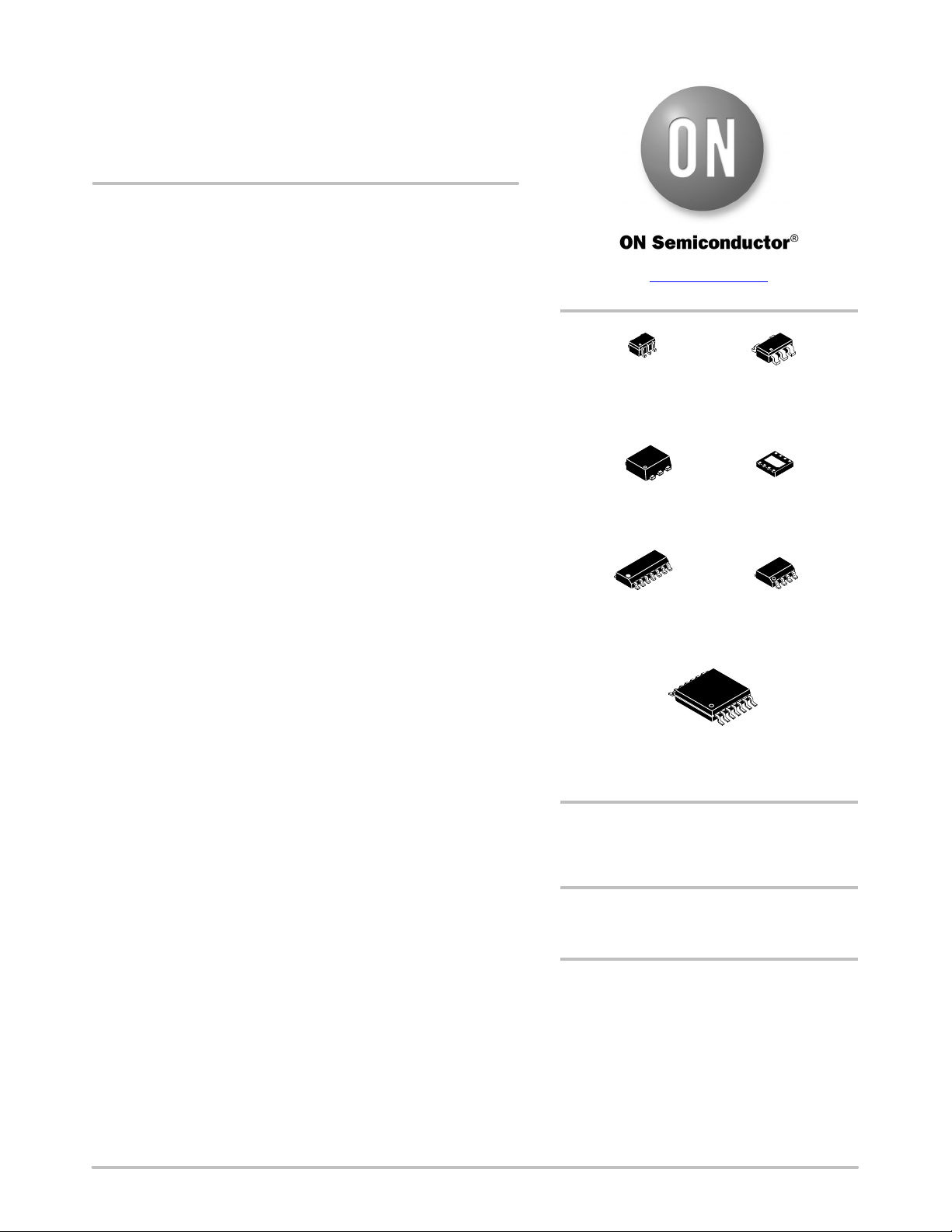
www.onsemi.com
The NCS2023x series of op amps feature a wide supply range of
2.7 V to 36 V with an input offset voltage as low as ±0.95 mV max.
These op amps are available in single, dual, and quad channel
configurations. Automotive qualified options are available under the
NCV prefix with an optional extended operating temperature range
from −40°C to 150°C. All other versions are specified over the
operating temperature range from −40°C to 125°C.
Features
• Supply Voltage Range: 2.7 V to 36 V
• Temperature Range: −40°C to 150°C
• Unity Gain Bandwidth: 3 MHz
• Input Offset Voltage: ±1.5 mV max, T
= −40 to 150°C
A
• Input Offset Voltage Drift: ±2 mV/°C max
• Common−Mode Input Voltage Range
♦ Optimal: V
♦ Functional: V
– 0.1 to VDD − 2 V
SS
– 0.1 to VDD + 0.1 V
SS
• NCV Prefix for Automotive and Other Applications Requiring
Unique Site and Control Change Requirements; AEC−Q100
Qualified and PPAP Capable
• These Devices are Pb−Free, Halogen Free/BFR Free and are RoHS
Compliant
Applications
• Telecom Equipment
• Power Supply Designs
• Diesel Injection Control
• Automotive
• Motor Control
5
1
SC−88A / SC70−5
CASE 419A−02
SOT−553, 5 LEAD
CASE 463B
14
1
SOIC−14 NB
CASE 751A−03
14
TSSOP−14 WB
CASE 948G
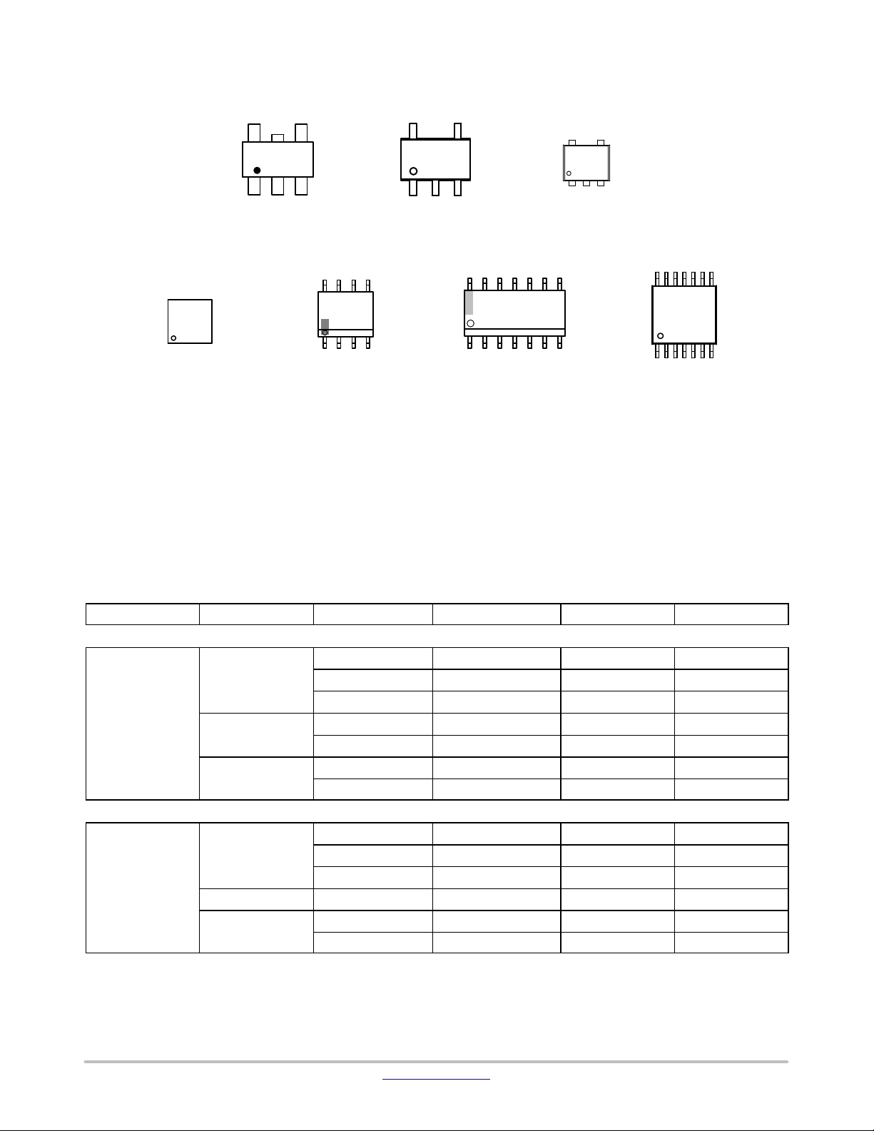
DEVICE MARKING INFORMATION
See general marking information in the device marking
section on page 2 of this data sheet.
PIN CONNECTIONS
See pin connections on page 3 of this data sheet.
5
1
TSOP−5
CASE 483
1
UDFN8
CASE 517AW
8
1
SOIC−8 NB
CASE 751−07
1
This document contains information on a product under development. ON Semiconductor
reserves the right to change or discontinue this product without notice.
© Semiconductor Components Industries, LLC, 2020
March, 2021 − Rev. P3
1 Publication Order Number:
ORDERING INFORMATION
See detailed ordering and shipping information on page 2 of
this data sheet.
NCS20231/D
Page 2
NCS20231, NCV20231, NCS20232, NCV20232, NCS20234, NCV20234
DEVICE MARKING INFORMATION
XX
YM
1
UDFN8, 2x2, 0.5P
CASE 517AW
XXAYWG
G
TSOP−5
CASE 483
XXMG
G
SC−88A / SC70−5
CASE 419A−02
8
XX
AYWW
G
1
SOIC−8 NB
CASE 751−07
XX = Specific Device Code
A = Assembly Location
Y = Year
W = Work Week
M = Date Code
G or G = Pb−Free Package
(Note: Microdot may be in either location)
14
1
CASE 751A−03
XXG
AWLYWW
SOIC−14 NB
XXMG
G
SOT−553, 5 LEAD
CASE 463B
14
XX
ALYWG
G
1
TSSOP−14 WB
CASE 948G
ORDERING INFORMATION
Temperature Channels Package Device Part Number Marking Shipping
Industrial and Commercial
−40°C to 125°C Single
Dual
Quad
Automotive Qualified, Grade 1
−40°C to 150°C
†For information on tape and reel specifications, including part orientation and tape sizes, please refer to our Tape and Reel Packaging
Specifications Brochure, BRD8011/D.
*In Development. Contact local sales office for more information.
Single
Dual SOIC−8 NCV20232DR2G** N232
Quad
TSOP−5 NCS20231SN2T1G** AAC
SC−88 NCS20231SQ3T2G** AAG
SOT−553 NCS20231XV53T2G** AC
SOIC−8 NCS20232DR2G** N232
UDFN−8 NCS20232MUTBG** DGA
SOIC−14 NCS20234DR2G**
TSSOP−14 NCS20234DBR2G**
TSOP−5 NCV20231SN2T1G** AAC
SC−88 NCV20231SQ3T2G** AAG
SOT−553 NCV20231XV53T2G** AC
SOIC−14 NCV20234DR2G**
TSSOP−14 NCV20234DBR2G**
†
www.onsemi.com
2
Page 3
NCS20231, NCV20231, NCS20232, NCV20232, NCS20234, NCV20234
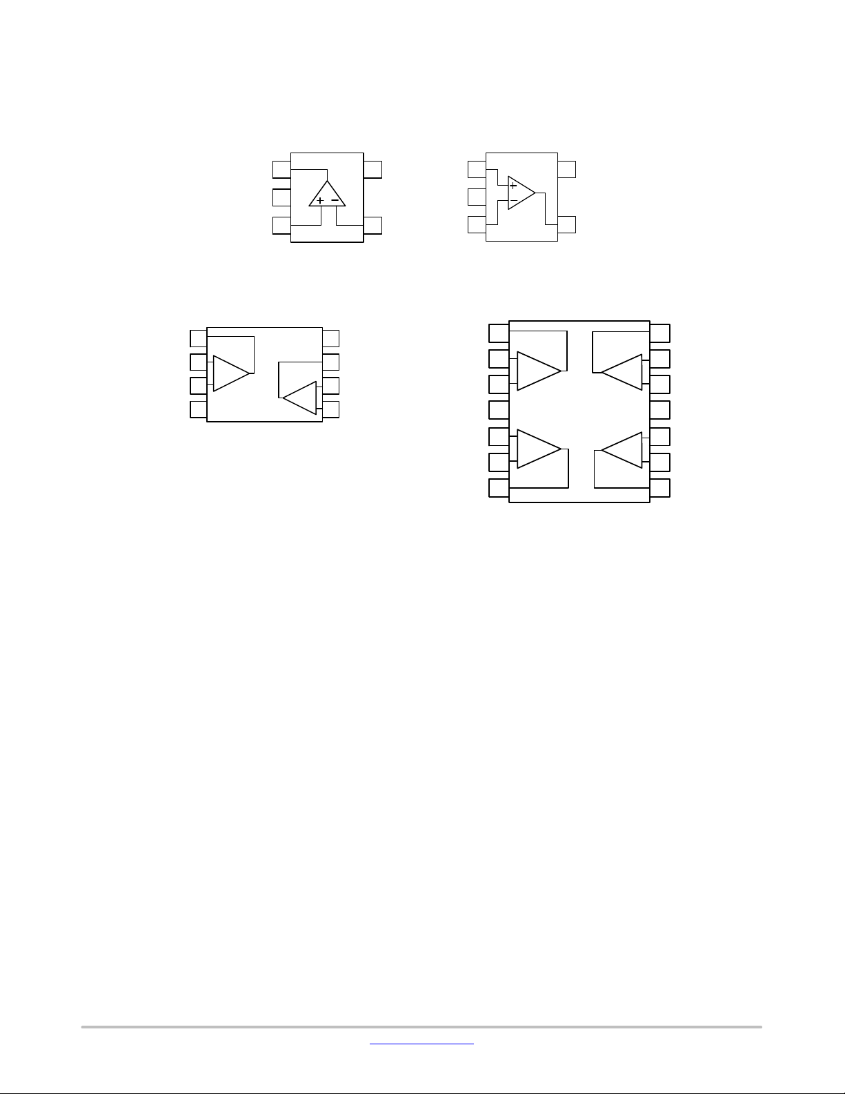
PIN CONNECTIONS
Single Channel
OUT 1
IN− 1
IN+ 1
VSS
OUT
VSS
Dual Channel Quad Channel
1
−
2
+
3
4
SOIC−8 / UDFN8
1
5
2
IN+
34
SOT23−5 / TSOP−5
8
VDD
7
OUT 2
6
IN− 2
−
+
IN+ 2
5
VDD
IN−
1
IN+
2
VSS
34
IN−
SOT−553 / SC−88
VDD
1
2
−
+
3
4
5
+
−
6
7
OUT 1
IN− 1
IN+ 1
IN+ 2
IN− 2
OUT 2
5
VDD
OUT
SOIC−14, TSSOP−14
14
OUT 4
IN− 4
13
−
+
+
−
12
11
10
9
8
IN+ 4
VSS
IN+ 3
IN− 3
OUT 3
www.onsemi.com
3
Page 4
NCS20231, NCV20231, NCS20232, NCV20232, NCS20234, NCV20234
ABSOLUTE MAXIMUM RATINGS (Note 1)
Parameter
Supply Voltage Range (VDD − VSS) V
Input Common−Mode Range V
Differential Input Voltage V
Maximum Input Current I
Maximum Output Current I
Continuous Total Power Dissipation P
Maximum Junction Temperature T
Storage Temperature Range T
ESD Capability, Human Body Model (Note 2) HBM ±2000 V
ESD Capability, Charge Device Model (Note 2) CDM ±1000 V
Latch Up Rating (Note 3) 100 mA
Moisture Sensitivity Level MSL Level 1
Lead Temperature Soldering
Reflow (SMD Styles Only), Pb−Free Versions (Note 4)
Stresses exceeding those listed in the Maximum Ratings table may damage the device. If any of these limits are exceeded, device functionality
should not be assumed, damage may occur and reliability may be affected.
1. Refer to ELECTRICAL CHARACTERISTICS and APPLICATION INFORMATION for Safe Operating Area
2. This device series incorporates ESD protection and is tested by the following methods:
ESD Human Body Model tested per JEDEC standard JS−001−2017 (AEC−Q100−002)
ESD Charged Device Model tested per JEDEC standard JS−002−2014 (AEC−Q100−011)
3. Latch−up Current tested per JEDEC standard JESD78E (AEC−Q100−004)
4. For information, please refer to our Soldering and Mounting Techniques Reference Manual, SOLDERRM/D
Symbol Value Unit
S
CM
ID
I
O
D
J(max)
STG
T
SLD
−0.3 to 40 V
VSS – 0.2 to VDD + 0.2 V
±V
S
±10 mA
±100 mA
200 mW
150 °C
−65 to 150 °C
260 °C
V
THERMAL CHARACTERISTICS
Parameter Symbol Package Value Unit
Thermal Resistance, Junction−to−Air
(Note 5)
q
JA
TSOP−5 TBD
SC88−5 TBD
°C/W
UDFN−8 TBD
SOIC−8 TBD
SOIC−14 TBD
TSSOP−14 TBD
5. Values based on copper area of 645 mm2 (or 1 in2) of 1 oz copper thickness and FR4 PCB substrate
RECOMMENDED OPERATING RANGES (Note 6)
Parameter
Supply Voltage (VDD − VSS) V
Differential Input Voltage V
Input Common−Mode Range V
Functional operation above the stresses listed in the Recommended Operating Ranges is not implied. Extended exposure to stresses beyond
the Recommended Operating Ranges limits may affect device reliability.
6. Refer to ELECTRICAL CHARACTERISTICS and APPLICATION INFORMATION for Safe Operating Area
Symbol Min Max Unit
S
ID
CM
2.7 36 V
±V
S
VSS – 0.1 VDD + 0.1 V
V
www.onsemi.com
4
Page 5
NCS20231, NCV20231, NCS20232, NCV20232, NCS20234, NCV20234
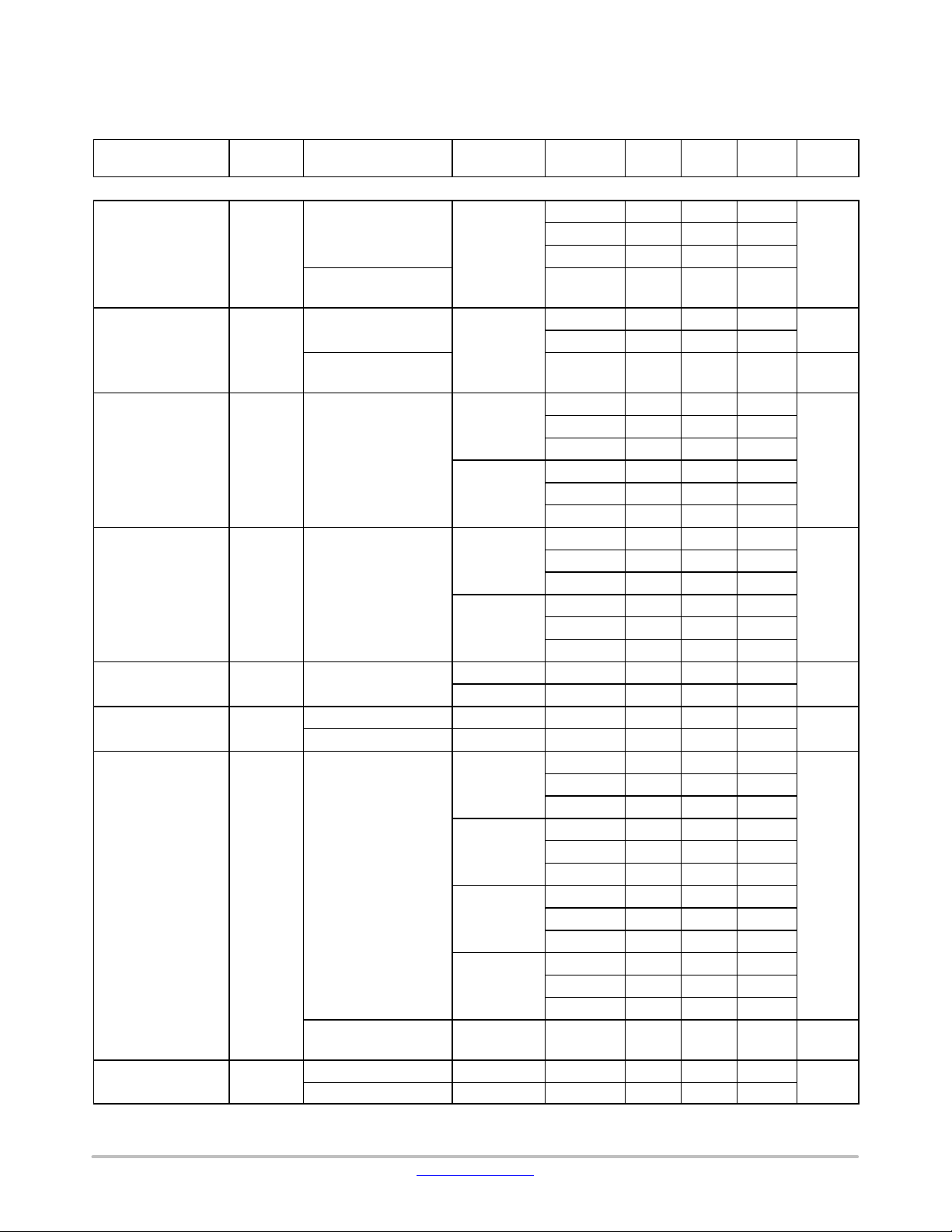
ELECTRICAL CHARACTERISTICS (V
At T
= +25°C, RL = 10 kW connected to midsupply, VCM = V
A
= 2.7 V to 36 V)
S
= midsupply, unless otherwise noted.
OUT
Boldface limits apply over the specified temperature range, guaranteed by characterization and/or design.
Supply
Parameter
Symbol Conditions
Voltage (V)
Temp (°C)
Min Typ Max Unit
INPUT CHARACTERISTICS
Offset Voltage
V
OS
VCM = mid−supply 2.7, 5, 10, 36
25 ±0.3 ±0.95
−40 to 125 ±1.5
−40 to 150 ±1.5
Offset Voltage Drift
dVOS/dT VCM = mid−supply 2.7, 5, 10, 36
over temp
Input Bias Current I
VCM = VDD – 2 V to
+ 0.1
V
DD
VCM = VDD – 2 V to
V
+ 0.1
DD
IB
2.7
25 ±7
−40 to 125 ±1 ±2 mV/°C
−40 to 150 ±1 ±5
−40 to 125 ±12
25 ±5 ±200
−40 to 125 ±3500
−40 to 150 ±9400
5, 10, 36
25 ±1 ±60
−40 to 125 ±3500
−40 to 150 ±9400
Input Offset Current I
OS
2.7
25 ±2 ±75
−40 to 125 ±500
−40 to 150 ±6000
5, 10, 36
25 ±0.5 ±60
−40 to 125 ±800
−40 to 150 ±6000
Channel Separation NCS20232,
NCS20234
Input Capacitance C
IN
Common mode 2.7, 36 25 TBD
2.7 25 TBD
5, 10, 36 25 100
Differential 2.7, 36 25 TBD
Common Mode
Rejection Ratio
CMRR VCM = VSS − 0.1 V to
− 2 V
V
DD
2.7
25 83 116
−40 to 125 69
−40 to 150 69
4
25 90 125
−40 to 125 80
−40 to 150 80
10
25 100 125
−40 to 125 80
−40 to 150 80
36
25 104 125
−40 to 125 80
−40 to 150 80
EMI Rejection Ratio EMIRR
VCM = VDD – 2 V
to V
+ 0.1 V
DD
f= 400 MHz 2.7, 36 25 70
2.7, 5, 10, 36 25 55 dB
f = 5 GHz 2.7, 36 25 90
mV
pA
pA
dB
pF
dB
dB
www.onsemi.com
5
Page 6

NCS20231, NCV20231, NCS20232, NCV20232, NCS20234, NCV20234
ELECTRICAL CHARACTERISTICS (V
At T
= +25°C, RL = 10 kW connected to midsupply, VCM = V
A
= 2.7 V to 36 V) (continued)
S
= midsupply, unless otherwise noted.
OUT
Boldface limits apply over the specified temperature range, guaranteed by characterization and/or design.
Supply
Parameter UnitMaxTypMin
ConditionsSymbol
Voltage (V)
Temp (°C)
OUTPUT CHARACTERISTICS
Open Loop Voltage
Gain
A
VOL
VCM = mid−supply 2.7
25 96 120
−40 to 125 86
−40 to 150 86
5
25 96 120
−40 to 125 86
−40 to 150 86
10
25 96 120
−40 to 125 86
−40 to 150 86
36
25 96 120
−40 to 125 86
−40 to 150 86
Open Loop Output
Impedance
High Level Output
Voltage Swing from
V
DD
Z
OUT
VDD−V
OH
VCM = VDD – 2 V
+ 0.1 V
to V
DD
RL = 10 kW
2.7, 5, 10, 36 25 60
2.7, 5, 10, 36
25 13 200
−40 to 125 250
−40 to 150 250
RL = 1 mA 2.7, 5, 10, 36
25 74 100
−40 to 125 150
−40 to 150 350
RL = 5 mA 10
25 180 200
−40 to 125 350 400
−40 to 150 400
Low Level Output
Voltage Swing from
V
SS
VOL−V
SS
RL = 10 kW
2.7, 5, 10
25 10 100
−40 to 125 150
−40 to 150 150
36
25 10 200
−40 to 125 250
−40 to 150 250
RL = 1 mA 2.7, 5, 10, 36
25 65 100
−40 to 125 300
−40 to 150 300
RL = 5 mA 10
25 180 200
−40 to 125 250 300
−40 to 150 300
See
Figure
dB
W
mV
mV
www.onsemi.com
6
Page 7

NCS20231, NCV20231, NCS20232, NCV20232, NCS20234, NCV20234
ELECTRICAL CHARACTERISTICS (V
At T
= +25°C, RL = 10 kW connected to midsupply, VCM = V
A
= 2.7 V to 36 V) (continued)
S
= midsupply, unless otherwise noted.
OUT
Boldface limits apply over the specified temperature range, guaranteed by characterization and/or design.
Supply
Parameter UnitMaxTypMin
ConditionsSymbol
Voltage (V)
Temp (°C)
OUTPUT CHARACTERISTICS
Output Current
Capability
I
OUT
Output to VDD rail,
sinking current
2.7 25 35
5 25 35
10 25 35
36 25 35
Output to VSS rail,
sourcing current
2.7 25 35
5 25 35
10 25 35
36 25 35
Capacitive Load
Drive
C
L
2.7 to 36 25 180 pF
DYNAMIC PERFORMANCE
Gain Bandwidth
Product
Gain Margin A
Phase Margin
Slew Rate SR
Settling Time to 0.1
%
GWBP
m
F
m
t
s
CL = 25 pF
CL = 25 pF, VCM = V
– 2 V to VDD + 0.1 V
2.7, 5, 10, 36 25
DD
CL = 25 pF 2.7, 5, 10, 36 25 14 dB
CL = 25 pF 2.7, 5, 10, 36 25 50 °
Unity gain, RL = 2 kW
Unity gain, VCM = V
– 2 V to VDD + 0.1 V
2.7, 5, 10, 36 25
DD
VIN = 1 V step 2.7 25 1.9 ms
VIN = 3 V step 5 25 1.2
VIN = 8 V step 10 25 3.4
VIN = 10 V step 36 25 3.2
Settling Time to 0.01
%
t
s
VIN = 1 V step 2.7 25 3.2 ms
VIN = 3 V step 5 25 5.6
VIN = 8 V step 10 25 6.8
VIN = 10 V step 36 25 7
NOISE PERFORMANCE
Total Harmonic
Distortion + Noise
Voltage Noise
Density
THD+ N
e
n
VIN = 0.5 Vpp,
f = 1 kHz, A
V
= 1
VIN = 2.5 Vpp,
f = 1 kHz, A
V
= 1
VIN = 7.5 Vpp,
f = 1 kHz, A
V
= 1
VIN = 28.5 Vpp,
f = 1 kHz, A
V
= 1
f = 1 kHz
f = 1 kHz, VCM = VDD –
2 V to V
DD
+ 0.1 V
2.7 25 0.009
5 25 0.009
10 25 0.004
36 25 0.004
2.7, 5, 10, 36 25
f = 10 kHz 20
Current Noise
Density
Voltage Noise, Peak
to Peak
i
n
e
pp
f = 1 kHz 2.7, 5, 10, 36 25 90 fA/√Hz
fIN = 0.1 Hz to 10 Hz
2.7, 5, 10, 36
25 TBD mV
fIN = 0.01 Hz to 1 Hz 25 TBD
mA
3
MHz
0.7
2.7 V/ms
0.7
%
30
nV/√Hz
30
pp
www.onsemi.com
7
Page 8

NCS20231, NCV20231, NCS20232, NCV20232, NCS20234, NCV20234
ELECTRICAL CHARACTERISTICS (V
At T
= +25°C, RL = 10 kW connected to midsupply, VCM = V
A
Boldface limits apply over the specified temperature range, guaranteed by characterization and/or design.
Parameter UnitMaxTypMin
POWER SUPPLY
Power Supply
Rejection Ratio
Quiescent Current I
Product parametric performance is indicated in the Electrical Characteristics for the listed test conditions, unless otherwise noted. Product
performance may not be indicated by the Electrical Characteristics if operated under different conditions.
PSRR Vs = 2.7 V to 36 V 2.7, 36
Q
= 2.7 V to 36 V) (continued)
S
ConditionsSymbol
No load, per channel 2.7, 5
= midsupply, unless otherwise noted.
OUT
Supply
Voltage (V)
10
36
Temp (°C)
25 11 4 135
−40 to 125 100
−40 to 150 90
25 0.475 0.595
−40 to 125 0.650
−40 to 150 0.7
25 0.475 0.595
−40 to 125 0.650
−40 to 150 0.75
25 0.475 0.595
−40 to 125 0.650
−40 to 150 0.8
dB
mA
www.onsemi.com
8
Page 9

NCS20231, NCV20231, NCS20232, NCV20232, NCS20234, NCV20234
PACKAGE DIMENSIONS
SC−88A (SC−70−5/SOT−353)
CASE 419A−02
B0.2 (0.008)
ISSUE L
NOTES:
1. DIMENSIONING AND TOLERANCING
PER ANSI Y14.5M, 1982.
2. CONTROLLING DIMENSION: INCH.
3. 419A−01 OBSOLETE. NEW STANDARD
419A−02.
4. DIMENSIONS A AND B DO NOT INCLUDE
MOLD FLASH, PROTRUSIONS, OR GATE
BURRS.
INCHES
DIMAMIN MAX MIN MAX
B 1.15 1.350.045 0.053
C 0.80 1.100.031 0.043
D 0.10 0.300.004 0.012
G 0.65 BSC0.026 BSC
H --- 0.10---0.004
J 0.10 0.250.004 0.010
K 0.10 0.300.004 0.012
N 0.20 REF0.008 REF
S 2.00 2.200.079 0.087
MILLIMETERS
1.80 2.200.071 0.087
J
A
G
45
D
5 PL
−B−
MM
S
12 3
N
C
H
K
SOLDER FOOTPRINT
0.50
0.0197
0.65
0.025
0.65
0.40
0.0157
1.9
0.0748
SCALE 20:1
*For additional information on our Pb−Free strategy and soldering
details, please download the ON Semiconductor Soldering and
Mounting Techniques Reference Manual, SOLDERRM/D.
0.025
mm
ǒ
inches
Ǔ
www.onsemi.com
9
Page 10

NCS20231, NCV20231, NCS20232, NCV20232, NCS20234, NCV20234
PACKAGE DIMENSIONS
TSOP−5
CASE 483
ISSUE M
NOTES:
1. DIMENSIONING AND TOLERANCING PER ASME
NOTE 5
2X
2X
T0.10
B
A
54
B
123
G
A
T0.20
D
0.205XC AB
M
S
K
DETAIL Z
TOP VIEW
J
DETAIL Z
C
0.05
H
SIDE VIEW
C
SEATING
PLANE
END VIEW
Y14.5M, 1994.
2. CONTROLLING DIMENSION: MILLIMETERS.
3. MAXIMUM LEAD THICKNESS INCLUDES LEAD FINISH
THICKNESS. MINIMUM LEAD THICKNESS IS THE
MINIMUM THICKNESS OF BASE MATERIAL.
4. DIMENSIONS A AND B DO NOT INCLUDE MOLD
FLASH, PROTRUSIONS, OR GATE BURRS. MOLD
FLASH, PROTRUSIONS, OR GATE BURRS SHALL NOT
EXCEED 0.15 PER SIDE. DIMENSION A.
5. OPTIONAL CONSTRUCTION: AN ADDITIONAL
TRIMMED LEAD IS ALLOWED IN THIS LOCATION.
TRIMMED LEAD NOT TO EXTEND MORE THAN 0.2
FROM BODY.
MILLIMETERS
DIM MIN MAX
A
2.85 3.15
B
1.35 1.65
C 0.90 1.10
D 0.25 0.50
G 0.95 BSC
H 0.01 0.10
J 0.10 0.26
K 0.20 0.60
M 0 10
__
S 2.50 3.00
SOLDERING FOOTPRINT*
1.9
0.95
0.037
1.0
0.039
*For additional information on our Pb−Free strategy and soldering
details, please download the ON Semiconductor Soldering and
Mounting Techniques Reference Manual, SOLDERRM/D.
0.074
0.028
0.7
2.4
0.094
SCALE 10:1
ǒ
inches
mm
Ǔ
www.onsemi.com
10
Page 11

NCS20231, NCV20231, NCS20232, NCV20232, NCS20234, NCV20234
PACKAGE DIMENSIONS
SOT−553, 5 LEAD
CASE 463B
ISSUE C
D
−X−
45
12 3
e
E
−Y−
b
5 PL
0.08 (0.003) X
M
A
L
H
E
c
Y
RECOMMENDED
SOLDERING FOOTPRINT*
0.3
0.0118
1.0
1.35
0.0531
0.0394
NOTES:
1. DIMENSIONING AND TOLERANCING PER ANSI Y14.5M, 1982.
2. CONTROLLING DIMENSION: MILLIMETERS
3. MAXIMUM LEAD THICKNESS INCLUDES LEAD FINISH
THICKNESS. MINIMUM LEAD THICKNESS IS THE MINIMUM
THICKNESS OF BASE MATERIAL.
DIMAMIN NOM MAX MIN
b 0.17 0.22 0.27 0.007
c
D 1.55 1.60 1.65 0.061
E 1.15 1.20 1.25 0.045
e 0.50 BSC
L 0.10 0.20 0.30 0.004
H
E
MILLIMETERS
0.50 0.55 0.60 0.020
0.08 0.13 0.18
1.55 1.60 1.65 0.061 0.063 0.065
INCHES
NOM MAX
0.022 0.024
0.009 0.011
0.003 0.005 0.007
0.063 0.065
0.047 0.049
0.020 BSC
0.008 0.012
0.45
0.0177
0.5
0.5
0.0197
0.0197
mm
ǒ
SCALE 20:1
inches
Ǔ
*For additional information on our Pb−Free strategy and soldering
details, please download the ON Semiconductor Soldering and
Mounting Techniques Reference Manual, SOLDERRM/D.
www.onsemi.com
11
Page 12

PIN ONE
REFERENCE
2X
2X
NOTE 4
DETAIL A
NCS20231, NCV20231, NCS20232, NCV20232, NCS20234, NCV20234
PACKAGE DIMENSIONS
UDFN8, 2x2
CASE 517AW
ISSUE A
B
C0.10
C0.10
C0.08
C0.10
TOP VIEW
SIDE VIEW
1
D2
D
DETAIL B
A1
4
A
L
L
L1
E
A
A3
DETAIL A
ALTERNATE
CONSTRUCTIONS
EXPOSED Cu
A1
MOLD CMPD
A3
DETAIL B
SEATING
C
PLANE
8X
L
E2
ALTERNATE
CONSTRUCTION
PACKAGE
OUTLINE
SOLDERING FOOTPRINT*
NOTES:
1. DIMENSIONING AND TOLERANCING PER
ASME Y14.5M, 1994.
2. CONTROLLING DIMENSION: MILLIMETERS.
3. DIMENSION b APPLIES TO PLATED
TERMINALS AND IS MEASURED BETWEEN
0.15 AND 0.30 MM FROM THE TERMINAL
TIP.
4. COPLANARITY APPLIES TO THE EXPOSED
PAD AS WELL AS THE TERMINALS.
5. FOR DEVICE OPN CONTAINING W OPTION,
DETAIL B ALTERNATE CONSTRUCTION IS
NOT APPLICABLE.
MILLIMETERS
DIM MIN MAX
A 0.45 0.55
A1 0.00 0.05
A3 0.13 REF
b 0.18 0.30
D 2.00 BSC
D2 1.50 1.70
E 2.00 BSC
E2 0.80 1.00
e 0.50 BSC
L 0.20 0.45
L1 −−− 0.15
RECOMMENDED
1.73
8X
0.50
8
e
e/2
BOTTOM VIEW
5
8X
b
0.10 C
0.05 C
A
BB
NOTE 3
1.00
0.50
PITCH
1
DIMENSIONS: MILLIMETERS
8X
0.30
2.30
*For additional information on our Pb−Free strategy and soldering
details, please download the ON Semiconductor Soldering and
Mounting Techniques Reference Manual, SOLDERRM/D.
www.onsemi.com
12
Page 13

−Y−
−Z−
NCS20231, NCV20231, NCS20232, NCV20232, NCS20234, NCV20234
PACKAGE DIMENSIONS
SOIC−8 NB
CASE 751−07
ISSUE AK
NOTES:
−X−
A
58
B
1
S
0.25 (0.010)
4
M
M
Y
K
G
C
SEATING
PLANE
0.10 (0.004)
H
D
0.25 (0.010) Z
M
SXS
Y
N
X 45
_
M
J
1. DIMENSIONING AND TOLERANCING PER
ANSI Y14.5M, 1982.
2. CONTROLLING DIMENSION: MILLIMETER.
3. DIMENSION A AND B DO NOT INCLUDE
MOLD PROTRUSION.
4. MAXIMUM MOLD PROTRUSION 0.15 (0.006)
PER SIDE.
5. DIMENSION D DOES NOT INCLUDE DAMBAR
PROTRUSION. ALLOWABLE DAMBAR
PROTRUSION SHALL BE 0.127 (0.005) TOTAL
IN EXCESS OF THE D DIMENSION AT
MAXIMUM MATERIAL CONDITION.
6. 751−01 THRU 751−06 ARE OBSOLETE. NEW
STANDARD IS 751−07.
MILLIMETERS
DIMAMIN MAX MIN MAX
4.80 5.00 0.189 0.197
B 3.80 4.00 0.150 0.157
C 1.35 1.75 0.053 0.069
D 0.33 0.51 0.013 0.020
G 1.27 BSC 0.050 BSC
H 0.10 0.25 0.004 0.010
J 0.19 0.25 0.007 0.010
K 0.40 1.27 0.016 0.050
M 0 8 0 8
____
N 0.25 0.50 0.010 0.020
S 5.80 6.20 0.228 0.244
INCHES
SOLDERING FOOTPRINT*
1.52
0.060
7.0
0.275
0.6
0.024
*For additional information on our Pb−Free strategy and soldering
details, please download the ON Semiconductor Soldering and
Mounting Techniques Reference Manual, SOLDERRM/D.
4.0
0.155
1.270
0.050
SCALE 6:1
ǒ
inches
mm
Ǔ
www.onsemi.com
13
Page 14

NCS20231, NCV20231, NCS20232, NCV20232, NCS20234, NCV20234
PACKAGE DIMENSIONS
SOIC−14 NB
CASE 751A−03
ISSUE L
14
H
M
0.25 B
0.10
DETAIL A
NOTES:
1. DIMENSIONING AND TOLERANCING PER
ASME Y14.5M, 1994.
2. CONTROLLING DIMENSION: MILLIMETERS.
3. DIMENSION b DOES NOT INCLUDE DAMBAR
PROTRUSION. ALLOWABLE PROTRUSION
SHALL BE 0.13 TOTAL IN EXCESS OF AT
MAXIMUM MATERIAL CONDITION.
4. DIMENSIONS D AND E DO NOT INCLUDE
MOLD PROTRUSIONS.
5. MAXIMUM MOLD PROTRUSION 0.15 PER
SIDE.
DIM MIN MAX MIN MAX
A 1.35 1.75 0.054 0.068
A1 0.10 0.25 0.004 0.010
A3 0.19 0.25 0.008 0.010
b 0.35 0.49 0.014 0.019
D 8.55 8.75 0.337 0.344
E 3.80 4.00 0.150 0.157
e 1.27 BSC 0.050 BSC
H 5.80 6.20 0.228 0.244
h 0.25 0.50 0.010 0.019
L 0.40 1.25 0.016 0.049
M 0 7 0 7
__ __
INCHESMILLIMETERS
D
A
B
8
A3
E
L
71
b
M
13X
M
0.25 B
S
A
C
S
A
e
A1
C
SEATING
PLANE
DETAIL A
h
X 45
_
M
SOLDERING FOOTPRINT*
6.50
1
14X
1.18
1.27
PITCH
14X
0.58
DIMENSIONS: MILLIMETERS
*For additional information on our Pb−Free strategy and soldering
details, please download the ON Semiconductor Soldering and
Mounting Techniques Reference Manual, SOLDERRM/D.
www.onsemi.com
14
Page 15

NCS20231, NCV20231, NCS20232, NCV20232, NCS20234, NCV20234
PACKAGE DIMENSIONS
TSSOP−14 WB
CASE 948G
ISSUE C
0.10 (0.004)
−T−
SEATING
PLANE
14X REFK
S
U
T
S
N
0.25 (0.010)
U0.15 (0.006) T
S
2X L/2
0.10 (0.004) V
14
M
8
M
L
PIN 1
IDENT.
1
S
U0.15 (0.006) T
A
−V−
B
N
−U−
F
7
DETAIL E
K
K1
J
J1
SECTION N−N
C
D
G
H
DETAIL E
NOTES:
1. DIMENSIONING AND TOLERANCING PER
ANSI Y14.5M, 1982.
2. CONTROLLING DIMENSION: MILLIMETER.
3. DIMENSION A DOES NOT INCLUDE MOLD
FLASH, PROTRUSIONS OR GATE BURRS.
MOLD FLASH OR GATE BURRS SHALL NOT
EXCEED 0.15 (0.006) PER SIDE.
4. DIMENSION B DOES NOT INCLUDE
INTERLEAD FLASH OR PROTRUSION.
INTERLEAD FLASH OR PROTRUSION SHALL
NOT EXCEED 0.25 (0.010) PER SIDE.
5. DIMENSION K DOES NOT INCLUDE DAMBAR
PROTRUSION. ALLOWABLE DAMBAR
PROTRUSION SHALL BE 0.08 (0.003) TOTAL
IN EXCESS OF THE K DIMENSION AT
MAXIMUM MATERIAL CONDITION.
6. TERMINAL NUMBERS ARE SHOWN FOR
REFERENCE ONLY.
7. DIMENSION A AND B ARE TO BE
DETERMINED AT DATUM PLANE −W−.
INCHESMILLIMETERS
−W−
DIM MIN MAX MIN MAX
A 4.90 5.10 0.193 0.200
B 4.30 4.50 0.169 0.177
C −−− 1.20 −−− 0.047
D 0.05 0.15 0.002 0.006
F 0.50 0.75 0.020 0.030
G 0.65 BSC 0.026 BSC
H 0.50 0.60 0.020 0.024
J 0.09 0.20 0.004 0.008
J1 0.09 0.16 0.004 0.006
K 0.19 0.30 0.007 0.012
K1 0.19 0.25 0.007 0.010
L 6.40 BSC 0.252 BSC
M 0 8 0 8
____
14X
0.36
SOLDERING FOOTPRINT
7.06
1
14X
1.26
0.65
PITCH
DIMENSIONS: MILLIMETERS
www.onsemi.com
15
Page 16

NCS20231, NCV20231, NCS20232, NCV20232, NCS20234, NCV20234
ON Semiconductor and are trademarks of Semiconductor Components Industries, LLC dba ON Semiconductor or its subsidiaries in the United States and/or other countries.
ON Semiconductor owns the rights to a number of patents, trademarks, copyrights, trade secrets, and other intellectual property. A listing of ON Semiconductor’s product/patent
coverage may be accessed at www.onsemi.com/site/pdf/Patent−Marking.pdf
ON Semiconductor makes no warranty, representation or guarantee regarding the suitability of its products for any particular purpose, nor does ON Semiconductor assume any liability
arising out of the application or use of any product or circuit, and specifically disclaims any and all liability, including without limitation special, consequential or incidental damages.
Buyer is responsible for its products and applications using ON Semiconductor products, including compliance with all laws, regulations and safety requirements or standards,
regardless of any support or applications information provided by ON Semiconductor. “Typical” parameters which may be provided in ON Semiconductor data sheets and/or
specifications can and do vary in different applications and actual performance may vary over time. All operating parameters, including “Typicals” must be validated for each customer
application by customer’s technical experts. ON Semiconductor does not convey any license under its patent rights nor the rights of others. ON Semiconductor products are not
designed, intended, or authorized for use as a critical component in life support systems or any FDA Class 3 medical devices or medical devices with a same or similar classification
in a foreign jurisdiction or any devices intended for implantation in the human body. Should Buyer purchase or use ON Semiconductor products for any such unintended or unauthorized
application, Buyer shall indemnify and hold ON Semiconductor and its officers, employees, subsidiaries, affiliates, and distributors harmless against all claims, costs, damages, and
expenses, and reasonable attorney fees arising out of, directly or indirectly, any claim of personal injury or death associated with such unintended or unauthorized use, even if such
claim alleges that ON Semiconductor was negligent regarding the design or manufacture of the part. ON Semiconductor is an Equal Opportunity/Affirmative Action Employer. This
literature is subject to all applicable copyright laws and is not for resale in any manner.
. ON Semiconductor reserves the right to make changes without further notice to any products herein.
PUBLICATION ORDERING INFORMATION
LITERATURE FULFILLMENT:
Email Requests to: orderlit@onsemi.com
ON Semiconductor Website: www.onsemi.com
◊
TECHNICAL SUPPORT
North American Technical Support:
Voice Mail: 1 800−282−9855 Toll Free USA/Canada
Phone: 011 421 33 790 2910
www.onsemi.com
Europe, Middle East and Africa Technical Support:
Phone: 00421 33 790 2910
For additional information, please contact your local Sales Representative
16
 Loading...