

Page 1
3 MHz, 125 mA Low Power
Operational Amplifier
NCS20061/2/4,
NCV20061/2/4
The NCS20061/2/4 is a family of single, dual and quad Operational
Amplifiers (Op Amps) with 3 MHz of Gain−Bandwidth Product
(GBWP) while consuming only 125 mA of Quiescent current per
opamp. The NCS2006x has Input Offset Voltage of 4 mV and operates
from 1.8 V to 5.5 V supply voltage over a wide temperature range
(−40°C to 125°C). The Rail−to−Rail In/Out operation allows the use of
the entire supply voltage range while taking advantage of the 3 MHz
GBWP. Thus, this family offers superior performance over many
industry standard parts. These devices are AEC−Q100 qualified which
is denoted by the NCV prefix.
NCS2006x’s low current consumption and low supply voltage
performance in space saving packages, makes them ideal for sensor
signal conditioning and low voltage current sensing applications in
Automotive, Consumer and Industrial markets.
Features
• Gain−Bandwidth Product: 3 MHz
• Low Supply Current/ Channel: 125 mA typ (V
• Low Input Offset Voltage: 4 mV max
• Wide Supply Range: 1.8 V to 5.5 V
• Wide Temperature Range: −40°C to +125°C
• Rail−to−Rail Input and Output
• Unity Gain Stable
• Available in Single, Dual and Quad Packages
• NCV Prefix for Automotive and Other Applications Requiring
Unique Site and Control Change Requirements; AEC−Q100
Qualified and PPAP Capable
• These Devices are Pb−Free, Halogen Free/BFR Free and are RoHS
Compliant
= 1.8 V)
S
www.onsemi.com
SC70−5
CASE 419A
Micro8]/MSOP8
CASE 846A
TSSOP−8
CASE 948S
14
1
SOIC−14
CASE 751A
5
1
TSOP−5/SOT23−5
CASE 483
8
1
SOIC−8
CASE 751
14
1
TSSOP−14
CASE 948G
6
1
UDFN6
CASE 517AP
Applications
• Automotive
• Battery Powered/ Portable
• Sensor Signal Conditioning
• Low Voltage Current Sensing
• Filter Circuits
• Unity Gain Buffer
© Semiconductor Components Industries, LLC, 2017
January, 2021 − Rev. 15
DEVICE MARKING INFORMATION
See general marking information in the device marking
section on page 2 of this data sheet.
ORDERING INFORMATION
See detailed ordering and shipping information on page 3 of
this data sheet.
1 Publication Order Number:
NCS2006/D
Page 2
NCS20061/2/4, NCV20061/2/4
MARKING DIAGRAMS
Single Channel Configuration
NCS20061, NCV20061
XXMG
G
SC70−5
CASE 419A
8
XXXX
AYW G
G
1
Micro8]/MSOP8
CASE 846A
14
XXXX
XXXX
ALYWG
G
1
TSSOP−14
CASE 948G
5
XXXAYWG
G
1
TSOP−5/SOT23−5
CASE 483
Dual Channel Configuration
NCS20062, NCV20062
8
XXXXXX
ALYW
G
1
SOIC−8
CASE 751
Quad Channel Configuration
NCS20064, NCV20064
14
XXXXXXXXG
AWLYWW
1
SOIC−14
CASE 751A
1
XX MG
G
UDFN6
CASE 517AP
XXX
YWW
AG
TSSOP−8
CASE 948S
XXXXX = Specific Device Code
A = Assembly Location
WL, L = Wafer Lot
Y = Year
WW, W = Work Week
G or G = Pb−Free Package
(Note: Microdot may be in either location)
www.onsemi.com
2
Page 3
NCS20061/2/4, NCV20061/2/4
Single Channel Configuration
NCS20061, NCV20061
1
OUT
2
VSS
+
3
IN+
SC70−5, SOT23−5 (TSOP−5)
SQ2, SN2 Pinout
OUT 1
IN− 1
IN+ 1
1
2
3
VSS
4
Micro8/MSOP8, SOIC−8, TSSOP−8
5
VDD
−
4
IN−
Dual Channel Configuration
NCS20062, NCV20062
−
+
−
+
1
IN+
+
VSS
2
−
3
IN−
SC70−5, SOT23−5 (TSOP−5)
SQ3, SN3 Pinout
8
VDD
7
OUT 2
6
IN− 2
IN+ 2
5
Figure 1. Pin Connections
5
VDD
4
OUT
Quadruple Channel Configuration
NCS20064, NCV20064
IN− 1
IN+ 1
VDD
IN+ 2
IN− 2
1
2
−
+
3
4
5
+
−
6
7
TSSOP−14, SOIC−14
OUT 1
OUT 2
VSS
NC
IN−
1
2
3
+
−
UDFN6 1.6 x 1.6
14
OUT 4
IN− 4
13
−
+
IN+ 4
12
VSS
11
IN+ 3
10
+
−
IN− 3
9
OUT 3
8
6
OUT
5
VDD
4
IN+
ORDERING INFORMATION
Device Configuration Automotive Marking Package Shipping
NCS20061SQ3T2G
NCS20061SN2T1G AEP SOT23−5/TSOP−5
NCS20061SN3T1G AEQ SOT23−5/TSOP−5
NCS20061MUTAG AG UDFN6
NCV20061SQ3T2G*
NCV20061SN2T1G* AEP SOT23−5/TSOP−5
NCV20061SN3T1G* AEQ SOT23−5/TSOP−5
NCS20062DMR2G
NCS20062DR2G NCS20062 SOIC−8
NCS20062DTBR2G K62 TSSOP−8
NCV20062DMR2G*
NCV20062DR2G* NCS20062 SOIC−8
NCV20062DTBR2G* K62 TSSOP−8
NCS20064DR2G
NCS20064DTBR2G 264 TSSOP−14
NCV20064DR2G*
NCV20064DTBR2G* 264 TSSOP−14
†For information on tape and reel specifications, including part orientation and tape sizes, please refer to our Tape and Reel Packaging
Specifications Brochure, BRD8011/D
*NCV Prefix for Automotive and Other Applications Requiring Unique Site and Control Change Requirements; AEC−Q100 Qualified and PPAP
Capable.
Single
Dual
Quad
No
Yes
No
Yes
No
Yes
AAM SC70
AAM SC70
2K62 Micro8/MSOP8
Contact local sales office for
more information
2K62 Micro8/MSOP8
20064 SOIC−14
20064 SOIC−14
†
www.onsemi.com
3
Page 4
NCS20061/2/4, NCV20061/2/4
ABSOLUTE MAXIMUM RATINGS (Note 1)
Rating
Supply Voltage (VDD – VSS) (Note 2) V
Input Voltage V
Differential Input Voltage V
Maximum Input Current I
Maximum Output Current I
Continuous Total Power Dissipation (Note 2) P
Maximum Junction Temperature T
Storage Temperature Range T
Mounting Temperature (Infrared or Convection – 20 sec) T
ESD Capability (Note 3) Human Body Model
Charge Device Model
Latch−Up Current (Note 4) I
Moisture Sensitivity Level (Note 5) MSL Level 1
Stresses exceeding those listed in the Maximum Ratings table may damage the device. If any of these limits are exceeded, device functionality
should not be assumed, damage may occur and reliability may be affected.
1. Refer to ELECTRICAL CHARACTERISTICS for Safe Operating Area.
2. Continuous short circuit operation to ground at elevated ambient temperature can result in exceeding the maximum allowed junction
temperature of 150°C. Output currents in excess of the maximum output current rating over the long term may adversely affect reliability.
Shorting output to either VDD or VSS will adversely affect reliability.
3. This device series incorporates ESD protection and is tested by the following methods:
ESD Human Body Model tested per JEDEC standard Js−001−2017 (AEC−Q100−002)
ESD Charged Device Model tested per JEDEC standard JS−002−2014 (AEC−Q100−011)
4. Latch−up Current tested per JEDEC standard JESD78E (AEC−Q100−004)
5. Moisture Sensitivity Level tested per IPC/JEDEC standard: J-STD-020A
Symbol Limit Unit
6 V
+ 0.5 V
DD
±V
s
±10 mA
±100 mA
200 mW
150 °C
−65 to 150 °C
260 °C
2000
2000
100 mA
V
V
ESD
ESD
S
I
ID
I
O
D
J
STG
mount
HBM
CDM
LU
VSS − 0.5 to V
THERMAL INFORMATION
Single Layer
Parameter Symbol Channels Package
Board (Note 6)
SC−70 490 444
Single
SOT23−5/TSOP−5 310 247
UDFN6 276 239
Junction to Ambient
Thermal Resistance
q
JA
Dual
Micro8/MSOP8 236 167
SOIC−8 190 131
TSSOP−8 253 194
SOIC−14 130 99
Quad
6. Value based on 1S standard PCB according to JEDEC51−3 with 1.0 oz copper and a 300 mm2 copper area
7. Value based on 1S2P standard PCB according to JEDEC51−7 with 1.0 oz copper and a 100 mm
TSSOP−14 178 140
2
copper area
Multi−Layer
Board (Note 7)
Unit
°C/W
OPERATING RANGES
Parameter Symbol Min Max Unit
Operating Supply Voltage V
Differential Input Voltage V
Input Common Mode Range V
Ambient Temperature T
S
ID
ICM
A
Functional operation above the stresses listed in the Recommended Operating Ranges is not implied. Extended exposure to stresses beyond
the Recommended Operating Ranges limits may affect device reliability.
1.8 5.5 V
V
S
VSS – 0.2 VDD + 0.2 V
−40 125 °C
V
www.onsemi.com
4
Page 5
NCS20061/2/4, NCV20061/2/4
ELECTRICAL CHARACTERISTICS AT VS = 1.8 V
TA = 25°C; RL ≥ 10 kW; VCM = V
Boldface limits apply over the specified temperature range, T
Parameter
INPUT CHARACTERISTICS
Input Offset Voltage
Offset Voltage Drift
Input Bias Current (Note 8) I
Input Offset Current (Note 8) I
Channel Separation XTLK f = 1 kHz 125 dB
Differential Input Resistance R
Common Mode Input Resistance R
Differential Input Capacitance C
Common Mode Input Capacitance C
Common Mode Rejection Ratio CMRR
OUTPUT CHARACTERISTICS
Open Loop Voltage Gain
Short Circuit Current I
Output Voltage High V
Output Voltage Low V
AC CHARACTERISTICS
Unity Gain Bandwidth UGBW 3 MHz
Slew Rate at Unity Gain SR VIN = 1.2 Vpp, Gain = 1 1.2
Phase Margin
Gain Margin A
Settling Time t
Open Loop Output Impedance Z
NOISE CHARACTERISTICS
Total Harmonic Distortion plus Noise THD+N VIN = 1.2 Vpp, f = 1 kHz, Av = 1 0.005 %
Input Referred Voltage Noise e
Input Referred Current Noise i
SUPPLY CHARACTERISTICS
Power Supply Rejection Ratio
Power Supply Quiescent Current I
8. Performance guaranteed over the indicated operating temperature range by design and/or characterization.
= mid−supply unless otherwise noted.
OUT
= −40°C to 125°C. (Note 8)
A
Symbol Conditions Min Typ Max Unit
V
OS
DVOS/DT
IB
OS
ID
IN
ID
CM
VCM = VSS – 0.2 to VDD + 0.2 48 73
VCM = VSS + 0.2 to VDD − 0.2 45
A
VOL
SC
Output to positive rail, sinking current 19
Output to negative rail, sourcing current 15
OH
OL
y
m
m
S
Voltage output swing from positive rail
Voltage output swing from negative rail
VIN = 1.2 Vpp,
Gain = 1
OL
n
n
PSRR No Load
DD
Per channel, no load 125 170
0.5 3.5 mV
4 mV
1
1 pA
1500 pA
1 pA
1100 pA
10
10
1 pF
5 pF
86 120
80
3 19
V
= VDD − V
OH
OUT
20
3 19
V
= V
OUT
− V
SS
20
OL
60 °
10 dB
Settling time to 0.1% 2.3 ms
Settling time to 0.01% 6
See
Figure
25
f = 1 kHz 20
f = 10 kHz 15
f = 1 kHz 300 fA/√Hz
67 90
64
mV/°C
V/ms
nV/√Hz
GW
GW
dB
dB
mA
mV
mV
W
dB
mA
www.onsemi.com
5
Page 6

NCS20061/2/4, NCV20061/2/4
ELECTRICAL CHARACTERISTICS AT VS = 3.3 V
TA = 25°C; RL ≥ 10 kW; VCM = V
Boldface limits apply over the specified temperature range, T
Parameter
INPUT CHARACTERISTICS
Input Offset Voltage
Offset Voltage Drift
Input Bias Current (Note 9) I
Input Offset Current (Note 9) I
Channel Separation XTLK f = 1 kHz 125 dB
Differential Input Resistance R
Common Mode Input Resistance R
Differential Input Capacitance C
Common Mode Input Capacitance C
Common Mode Rejection Ratio CMRR
OUTPUT CHARACTERISTICS
Open Loop Voltage Gain
Short Circuit Current I
Output Voltage High V
Output Voltage Low V
AC CHARACTERISTICS
Unity Gain Bandwidth UGBW 3 MHz
Slew Rate at Unity Gain SR VIN = 2.5 Vpp, Gain = 1 1.2
Phase Margin
Gain Margin A
Settling Time t
Open Loop Output Impedance Z
NOISE CHARACTERISTICS
Total Harmonic Distortion plus Noise THD+N VIN = 2.5 Vpp, f = 1 kHz, Av = 1 0.005 %
Input Referred Voltage Noise e
Input Referred Current Noise i
SUPPLY CHARACTERISTICS
Power Supply Rejection Ratio
Power Supply Quiescent Current I
9. Performance guaranteed over the indicated operating temperature range by design and/or characterization.
= mid−supply unless otherwise noted.
OUT
= −40°C to 125°C. (Note 9)
A
Symbol Conditions Min Typ Max Unit
V
OS
DVOS/DT
IB
OS
ID
IN
ID
CM
VCM = VSS – 0.2 to VDD + 0.2 53 76
VCM = VSS + 0.2 to VDD − 0.2 48
A
VOL
SC
Output to positive rail, sinking current 19
Output to negative rail, sourcing current 15
OH
OL
y
m
m
S
Voltage output swing from positive rail
Voltage output swing from negative rail
VIN = 2.5 Vpp,
Gain = 1
OL
n
n
PSRR No Load
DD
Per channel, no load 135 180
0.5 3.5 mV
4 mV
1
1 pA
1500 pA
1 pA
1100 pA
10
10
1 pF
5 pF
90 120
86
3 24
V
= VDD − V
OH
OUT
25
3 24
V
= V
OUT
− V
SS
25
OL
60 °
10 dB
Settling time to 0.1% 2.3 ms
Settling time to 0.01% 3.1
See
Figure
25
f = 1 kHz 20
f = 10 kHz 15
f = 1 kHz 300 fA/√Hz
67 90
64
mV/°C
V/ms
nV/√Hz
GW
GW
dB
dB
mA
mV
mV
W
dB
mA
www.onsemi.com
6
Page 7
NCS20061/2/4, NCV20061/2/4
ELECTRICAL CHARACTERISTICS AT VS = 5.5 V
TA = 25°C; RL ≥ 10 kW; VCM = V
Boldface limits apply over the specified temperature range, T
Parameter
INPUT CHARACTERISTICS
Input Offset Voltage
Offset Voltage Drift
Input Bias Current (Note 10) I
Input Offset Current (Note 10) I
Channel Separation XTLK f = 1 kHz 125 dB
Differential Input Resistance R
Common Mode Input Resistance R
Differential Input Capacitance C
Common Mode Input Capacitance C
Common Mode Rejection Ratio CMRR
OUTPUT CHARACTERISTICS
Open Loop Voltage Gain A
Short Circuit Current I
Output Voltage High V
Output Voltage Low V
AC CHARACTERISTICS
Unity Gain Bandwidth
Slew Rate at Unity Gain SR VIN = 5 Vpp, Gain = 1 1.2
Phase Margin
Gain Margin A
Settling Time t
Open Loop Output Impedance Z
NOISE CHARACTERISTICS
Total Harmonic Distortion plus Noise THD+N VIN = 5 Vpp, f = 1 kHz, Av = 1 0.005 %
Input Referred Voltage Noise e
Input Referred Current Noise i
SUPPLY CHARACTERISTICS
Power Supply Rejection Ratio
Power Supply Quiescent Current I
10.Performance guaranteed over the indicated operating temperature range by design and/or characterization.
Product parametric performance is indicated in the Electrical Characteristics for the listed test conditions, unless otherwise noted. Product
performance may not be indicated by the Electrical Characteristics if operated under different conditions.
= mid−supply unless otherwise noted.
OUT
= −40°C to 125°C. (Note 10)
A
Symbol Conditions Min Typ Max Unit
V
OS
DVOS/DT
IB
OS
ID
IN
ID
CM
VCM = VSS – 0.2 to VDD + 0.2 55 79
VCM = VSS + 0.2 to VDD − 0.2 51
VOL
SC
Output to positive rail, sinking current 19
Output to negative rail, sourcing current 15
OH
OL
Voltage output swing from positive rail
Voltage output swing from negative rail
UGBW 3 MHz
y
m
m
S
VIN = 5 Vpp,
Gain = 1
OL
n
n
PSRR No Load
DD
Per channel, no load 140 200
0.5 3.5 mV
4 mV
1
1 pA
1500 pA
1 pA
1100 pA
10
10
1 pF
5 pF
90 120
86
3 24
V
= VDD − V
OH
OUT
25
3 24
V
= V
OUT
− V
SS
25
OL
60 °
10 dB
Settling time to 0.1% 2.3
Settling time to 0.01% 3.1
See
Figure
25
f = 1 kHz 20
f = 10 kHz 15
f = 1 kHz 300 fA/√Hz
67 90
64
mV/°C
GW
GW
dB
dB
mA
mV
mV
V/ms
ms
W
nV/√Hz
dB
mA
www.onsemi.com
7
Page 8
NCS20061/2/4, NCV20061/2/4
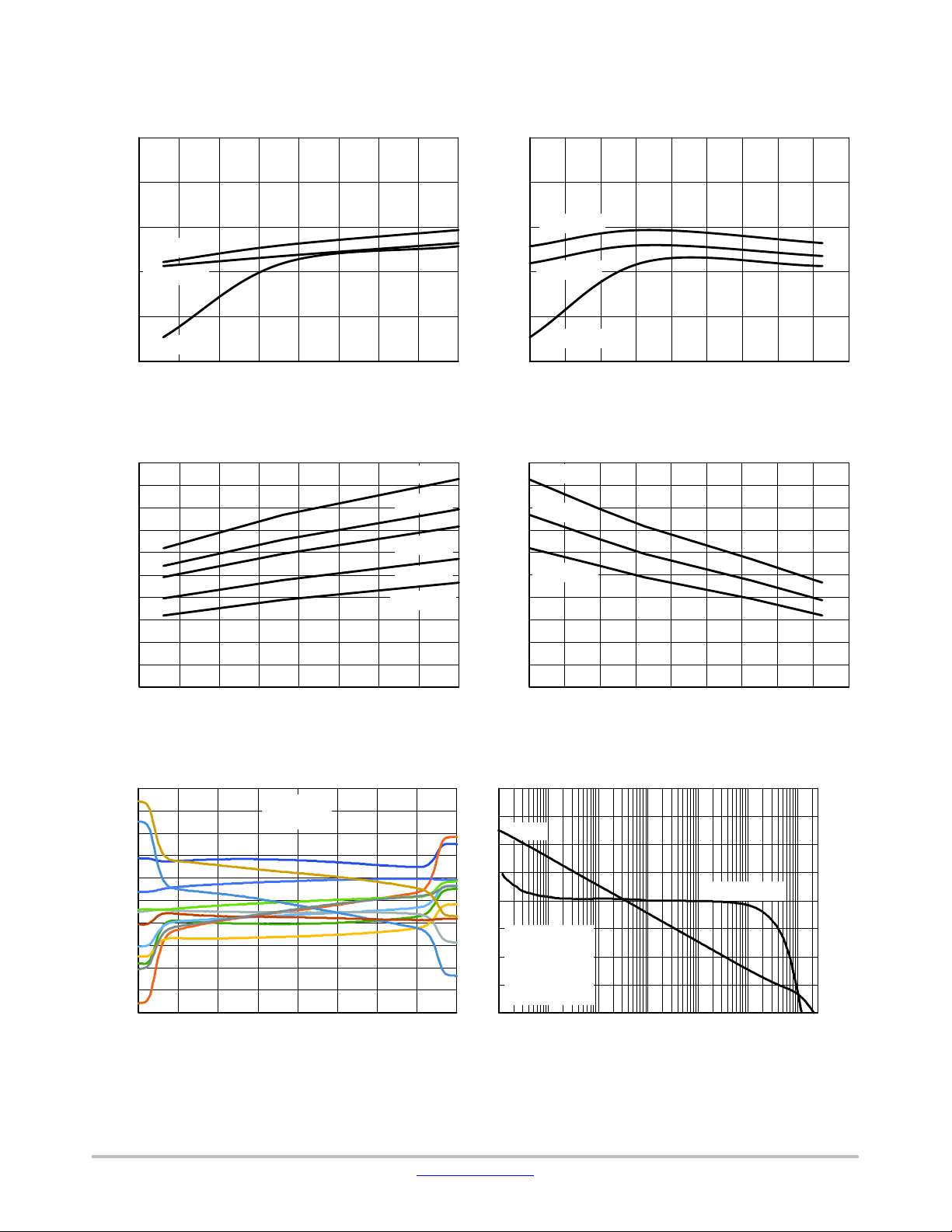
TYPICAL PERFORMANCE CHARACTERISTICS
TA = 25°C, RL ≥ 10 kW, VCM = V
= mid−supply unless otherwise specified
OUT
SUPPLY CURRENT (mA)
1000
OFFSET VOLTAGE (mV)
180
160
140
T = 25°C
120
T = 125°C
100
T = −40°C
80
SUPPLY VOLTAGE (V) TEMPERATURE (°C)
Figure 2. Quiescent Current per Channel vs.
5.5
5.04.54.03.53.02.52.01.5
180
160
VS = 5.5 V
140
VS = 3.3 V
120
SUPPLY CURRENT (mA)
100
VS = 1.8 V
80
60 140
Figure 3. Quiescent Current vs. Temperature
Supply Voltage
1000
OFFSET VOLTAGE (mV)
900
800
700
600
500
400
300
200
100
VS = 5.5 V
VS = 3.3 V
VS = 1.8 V
0
40 140
900
800
700
600
500
400
300
200
100
T = −40°C
T = 0°C
T = 25°C
T = 85°C
T = 125°C
0
SUPPLY VOLTAGE (V) TEMPERATURE (°C)
5.04.54.03.53.02.52.01.5
5.5
Figure 4. Offset Voltage vs. Supply Voltage Figure 5. Offset Voltage vs. Temperature
1201008040200−20−40
1201008060200−20−40
2000
1600
1200
800
400
−400
−800
OFFSET VOLTAGE (mV)
−1200
−1600
−2000
VS = 5.5 V
12 units
0
COMMON MODE VOLTAGE (V) FREQUENCY (Hz)
Figure 6. Offset Voltage vs. Common Mode
Voltage
140
120
100
80
60
GAIN (dB)
40
AV−10
V
20
R
C
0
−22 dBm Input
2.11.40.70−0.7−1.4−2.1−2.8
−20
2.8
www.onsemi.com
8
Gain
Phase Margin
= 5.5 V
S
= 10 kW
L
= 15 pF
L
Figure 7. Open−loop Gain and Phase Margin
vs. Frequency
180
135
90
PHASE MARGIN (°)
45
0
10M1M100k10k1k10010
Page 9
NCS20061/2/4, NCV20061/2/4
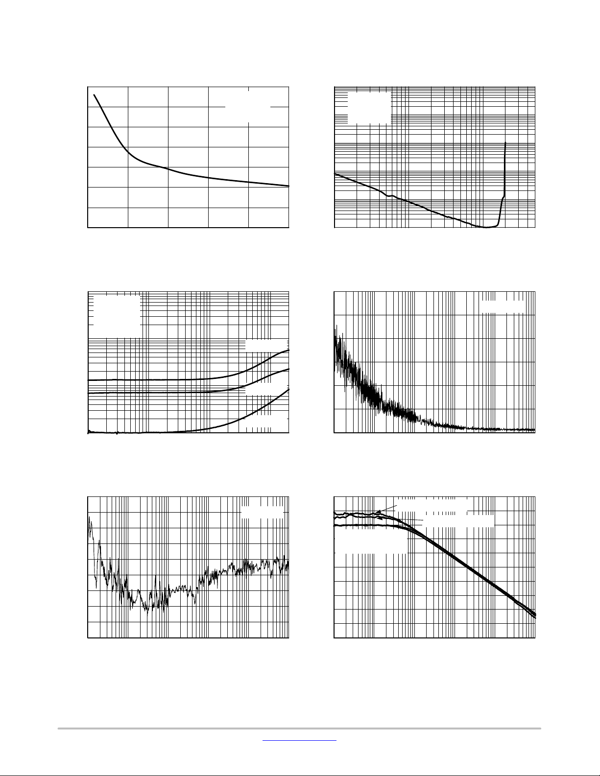
TYPICAL PERFORMANCE CHARACTERISTICS
TA = 25°C, RL ≥ 10 kW, VCM = V
= mid−supply unless otherwise specified
OUT
70
VS = 5.5 V
R
60
= 10 kW
L
T = 25°C
50
40
30
20
PHASE MARGIN (°)
10
0
5004003002001000
100
10
1
0.1
THD+N (%)
0.01
0.001
VS = 5.5 V
= 1 kHz
f
IN
A
= 1
V
10.10.01
CAPACITIVE LOAD (pF) OUTPUT VOLTAGE (Vrms)
Figure 8. Phase Margin vs. Capacitive Load Figure 9. THD + N vs. Output Voltage
1
0.1
AV = 1 V/V
R
= 10 kW
L
T
= 25°C
A
1 V
RMS
VS = 1.8 V
600
VS = 5.5 V
500
400
300
THD+N (%)
0.01
VS = 3.3 V
VOLTAGE NOISE (nV/√Hz)
200
100
VS = 5.5 V
0.001
0
10k1k10010
FREQUENCY (Hz) FREQUENCY (Hz)
Figure 10. THD + N vs. Frequency Figure 11. Input Voltage Noise vs. Frequency
100
90
80
VS = 1.8 V, PSRR+
70
VS = 1.8 V, PSRR−
60
50
40
PSRR (dB)
30
20
10
0
VS = 5.5 V, PSRR+
VS = 5.5 V, PSRR−
CURRENT NOISE (fA/√Hz)
900
800
700
600
500
400
300
200
100
VS = 5.5 V
0
100k10k1k100101
FREQUENCY (Hz) FREQUENCY (Hz)
Figure 12. Input Current Noise vs. Frequency Figure 13. PSRR vs. Frequency
100k10k1k100101
1M100k10k1k10010
www.onsemi.com
9
Page 10

NCS20061/2/4, NCV20061/2/4
TYPICAL PERFORMANCE CHARACTERISTICS
TA = 25°C, RL ≥ 10 kW, VCM = V
= mid−supply unless otherwise specified
OUT
120
VS = 5.5 V
100
VS = 3.3 V
80
VS = 1.8 V
60
CMRR (dB)
40
20
0
500
400
300
200
100
0
OUTPUT VOLTAGE TO NEGATIVE RAIL (mV)
Figure 16. Output Voltage Low to Rail Figure 17. Non−Inverting Small Signal
300
AV = 1
250
200
150
RAIL (mV)
100
50
OUTPUT VOLTAGE TO POSITIVE
0
1M100k10k1k10010
FREQUENCY (Hz) OUTPUT CURRENT (mA)
VS = 1.8 V
VS = 3.3 V
VS = 5.5 V
Figure 14. CMRR vs. Frequency Figure 15. Output Voltage High to Rail
0.100
0.075
20151050
0.050
0.025
−0.025
VOLTAGE (V)
−0.050
−0.075
−0.100
0
3210−1
TIME (ms)
VS = 1.8 V
VS = 3.3 V
VS = 5.5 V
OUTPUT CURRENT (mA)
Transient Response
15.012.510.07.55.02.50
4
0.100
0.075
0.050
0.025
−0.025
VOLTAGE (V)
−0.050
−0.075
−0.100
0
56
TIME (ms) TIME (ms)
Figure 18. Inverting Small Signal Transient
Response
1.5
1.0
0.5
0
VOLTAGE (V)
−0.5
−1.0
−1.5
8
743210−1−2
www.onsemi.com
10
543210−1
Figure 19. Non−Inverting Large Signal
Transient Response
6
Page 11

NCS20061/2/4, NCV20061/2/4
TYPICAL PERFORMANCE CHARACTERISTICS
TA = 25°C, RL ≥ 10 kW, VCM = V
= mid−supply unless otherwise specified
OUT
1.5
1.0
0.5
0
VOLTAGE (V)
−0.5
−1.0
−1.5
543210−1−2
TIME (ms)
Figure 20. Inverting Large Signal Transient
Response
18
16
14
12
10
8
6
4
I
2
CURRENT (pA)
OS
0
I
IB+
−2
−4
I
IB−
−6
−0.5 5.5
0.5 1.5 2.5 4.5 6.0
COMMON MODE VOLTAGE (V) TIME (s)
Figure 22. Input Bias Current vs. Common
Mode Voltage
67
5.04.03.53.02.01.00
8
600
500
400
300
200
CURRENT (pA)
100
0
−100
Figure 21. Input Bias and Offset Current vs.
6
4
2
0
−2
VOLTAGE (mV)
−4
−6
I
IB+
I
IB−
I
OS
80 140
1201006040200−20−40
TEMPERATURE (°C)
Temperature
3710
98654210
Figure 23. 0.1 Hz to 10 Hz Noise
−60
100k
−80
10k
−100
V
S
= 3.3 V
1k
−120
OUTPUT IMPEDANCE (W)
CHANNEL SEPARATION (dB)
−140
10M1M100k10k1k100
FREQUENCY (Hz)
100
10 100 1k 10k 100k 1M 10M
FREQUENCY (Hz)
Figure 24. Channel Separation vs. Frequency Figure 25. Open Loop Output Impedance
vs. Frequency
www.onsemi.com
11
V
S
V
S
= 1.8 V
= 5.5 V
Page 12

NCS20061/2/4, NCV20061/2/4
TYPICAL PERFORMANCE CHARACTERISTICS
TA = 25°C, RL ≥ 10 kW, VCM = V
1.5
SR+
1.4
1.3
1.2
SR−
SLEW RATE (V/ms)
1.1
= mid−supply unless otherwise specified
OUT
1.0
40 140
TEMPERATURE (°C)
Figure 26. Slew Rate vs. Temperature
1201008060200−20−40
www.onsemi.com
12
Page 13

NCS20061/2/4, NCV20061/2/4
Application Information
The NCS/NCV20061/2/4 family of operational
amplifiers is manufactured using ON Semiconductor’s
CMOS process. Products in this class are general purpose,
unity−gain stable amplifiers and include single, dual and
quad configurations.
Rail−to−Rail Input with No Phase Reversal
The NCS operational amplifiers are designed to prevent
phase reversal or any similar issues when the input pins
potential exceed the supply voltages by up to 100 mV.
Figure 6 shows the input voltage exceeding the supply
limits.
The input stage of the NCS/NCV 20061/2/4 family
consists of two differential CMOS input stages connected in
parallel: the first is constructed using paired PMOS devices
and it operates at low common mode input voltages (VCM);
the second stage is build using paired NMOS devices to
operate at high VCM. The transition between the two input
stages occurs at a common mode input voltage of
approximately VDD–1.3V and it is visible in Figure 6
(Offset vs. VCM).
Limiting input voltages
In order to prevent damage and/or improper operation of
these amplifiers, the application circuit must never expose
the input pins to voltages or currents higher than the
Absolute Maximum Ratings.
The internal ESD structure includes special diodes to
protect the input stages while maintaining a low Input Bias
(IIB) current. The input protection circuitry clamp the inputs
when the signals applied exceed more than one diode drop
below VSS or one diode drop above VDD. Very fast ESD
events (within the limits specified) trigger the protection
structure so the operational amplifier is not damaged.
However, in some applications, it can be necessary to
prevent excessive voltages from reaching the operational
amplifier inputs by adding external clamp diodes. A possible
solution is presented in Figure 27, where the four low−drop
fast diodes (Shottky preferred) are used in parallel with the
internal structure to divert the excessive energy to the supply
rails where it can be easily dissipated or absorbed by the
supply capacitors. The application designer should also take
into account that these external diodes add leakage currents
and parasitic capacitance that must be considered when
evaluating the end−to−end performance of the amplifier
stage.
Limiting input currents
In order to prevent damage/ improper operation of these
amplifiers, the application circuit must limit the currents
flowing in and out of the input pins. A possible solution is
presented in Figure 27 by means of the two added series
resistors. The minimum value for R_IN− and R_IN+ should
be calculated using Ohm’s Law so they limit the input pin
currents to less than the absolute maximum values specified.
The application designer should take into account that these
resistors also add parasitic inductance that must be
considered when evaluating performance.
Combining the current limiting resistors with the voltage
limiting diodes creates a solid input protection structure, that
can be used to insure reliable operation of the amplifier even
in the hardest conditions.
Figure 27. Typical Protection of the Operational Amplifier Inputs
Rail−to−Rail Output
The maximum output voltage swing is dependent of the
particular output load. According to the specification, the
output can reach within 25 mV of either supply rail when
load resistance is 10 kΩ. Figure 15 and Figure 16 shows the
load drive capabilities of the part under different conditions.
Output current is internally limited to 15 mA typ.
Capacitive Loads
Driving capacitive loads can create stability problems for
voltage feedback opamps, as it is a known possible cause for:
www.onsemi.com
• degraded phase margin
• lowered bandwidth
• gain peaking of the frequency response
• overshoot and ringing of the step response.
While the NCS/NCV20061/2/4 family of opamps are
capable of driving capacitive loads up to 100pF, adding a
small resistor in series to the output (R_ISO in Figure 28)
will increase the feedback loop’s phase margin. This leads
to higher stability by making the equivalent load more
resistive at high frequencies.
13
Page 14

NCS20061/2/4, NCV20061/2/4
Figure 28. Driving Capacitive Loads
Simulating the application with ON Semiconductor’s
P−SPICE models is a good starting point for selecting the
isolation resistor’s value, and then bench testing the
frequency and step response can be used to fine−tune the
value according to the desired characteristic.
Unity Gain Bandwidth
Interfacing a high impedance sensor’s output to a
relatively low−impedance ADC input usually requires an
intermediate stage to avoid unwanted interference of the two
devices, and this stage needs to have a high input impedance,
a low output impedance and high output current.
The unity gain buffer is recommended here (Figure 29).
The ADC’s internal sampling capacitor requires a buffer
front−end to recharge it faster than the sampling time, and
this problem is even worse if more channels are sampled by
the same ADC using an internal multiplexer. In order to
achieve a settling time shorter than the multiplexed
sampling rate, an RC stage is recommended between the
buffer and the ADC input. The R resistor’s value should be
low enough to charge the capacitor quickly, but at the same
time large enough to isolate the capacitive load from the
opamp’s output to preserve phase margin. When transients
are generated by the sensor’s output, first the two opamp’s
inputs see a high differential voltage between them, then the
output settles and brings the inverting input back to the
correct voltage.
To successfully accommodate for example a 0.1 V to 4 V
sensor signal, the opamp’s differential input range of the
NCS(V) 20061/2/4 series is close to the supply range
VDD−VSS, and the output will match the input. The
differential input voltage is limited only by the ESD
protection structure and not by back−to−back diodes
between inputs.
Figure 29. Unity Gain Buffer Stage for Sampling with ADC
Power Supply Bypassing
For AC, the power supply pins (VDD and VSS for split
supply, VDD for single supply) should be bypassed locally
with a quality capacitor in the range of 100 nF (ceramics are
recommended for their low ESR and good high frequency
response) as close as possible to the opamp’s supply pins.
For DC, a bulk capacitor in the range of 1 mF within inches
distance from the opamp can provide the increased currents
required to drive higher loads.
Unused Operational Amplifiers
Occasionally not all the opamps offered in the quad
packages are needed for a specific application. They can be
connected as “buffering ground” as shown in Figure 30, a
solution that does not need any extra parts. Connecting them
differently (inputs split to rails, left floating, etc.) can
sometimes cause unwanted oscillation, crosstalk, increased
current consumption, or add noise to the supply rails.
Figure 30. Unused Operational Amplifiers
PCB Surface Leakage
The Printed Circuit Board’s surface leakage effects should
be estimated if the lowest possible input bias current is
critical. Dry environment surface current increases further
when the board is exposed to humidity, dust or chemical
contamination. For harsh environment conditions,
protecting the entire board surface (with all the exposed
metal pins and soldered areas) is advised. Conformal coating
or potting the board in resin proves effective in most cases.
www.onsemi.com
14
Page 15

NCS20061/2/4, NCV20061/2/4
An alternate solution for reduced leakage is the use of
guard rings around sensitive pins and pads. A proper guard
ring should have low impedance and be biased to the same
voltage as the sensitive pin so no current flows in between.
For an inverting amplifier, the non−inverting input is
usually connected to supply’s ground (or virtual ground at
half the rail voltage in single supply applications) so it can
represent a good ring solution. When routing the PCB traces,
create a closed perimeter around the inverting input pad (which
carries the signal) and connect it to the non−inverting input.
For a non−inverting amplifier, use a similarly shaped
(rectangle or circle) copper trace around the non−inverting
input pad (which carries the signal) and connect it to the
inverting input pin, which presents a much lower impedance
thanks to the feedback network.
PCB Routing Recommendations
Even when some operational amplifier is expected to
amplify only the useful DC signal, it can also pick some high
frequency noise altogether and amplify it accordingly, if the
design allows it. In order to reach the specified operational
amplifier parameters and to avoid high frequency
Applications Example
interference issues, it is recommended that the PCB layout
respects some basic guidelines:
• A dedicated layer for the ground plane should be used
whenever possible and all supply decoupling capacitors
should connect to it by vias.
• Copper traces should be as short as possible.
• High current paths should not be shared by small signal
or low current traces.
• If present, switching power supply blocks should be
kept away from the analog sensitive areas to avoid
potential conducted and radiated noise issues.
• When different circuit taxonomies share the same
board, it is recommended to keep separated the power
areas, the digital areas and the small signal analog
areas. Small−signal parts in the signal path should be
placed as close as possible to the opamp’s input pins.
• Metal shielding the sensitive areas and the “offender”
blocks may be required in some cases.
In a sensitive application, a good PCB design can take longer
but it will save troubleshooting time.
Second Order Active Low Pass Filter
Using an opamp with a low input bias current allows the
use of higher value resistors and smaller capacitors for the
same filter application. As a trade−off for the increased
impedance and lower consumption obtained, the higher
value resistors may also bring higher noise and sensibility to
board contamination, and possibly frequency response
changes (the increased R*C time constant due to parasitic
capacitances can change the gain vs. frequency plot).
An example of an active low−pass filter using the
NCS2006x operational amplifier can be found in Figure 31.
The filter’s 3 dB Bandwidth is approximately 25 KHz,
followed by a −40 dB/dec roll−off as in Figure 32. Such
filters with flat response in the sampled signal band are
recommended as a front−end for ADC’s to avoid aliasing.
Figure 32. Filter’s Frequency Response
Using the P−SPICE models provided by
ON Semiconductor is recommended as a starting point for
component selection, and then values can be further
fine−tuned during bench testing the application.
Figure 31. Second Order Active Low Pass Filter
Micro8 is a trademark of International Rectifier
www.onsemi.com
15
Page 16

MECHANICAL CASE OUTLINE
PACKAGE DIMENSIONS
SC−88A (SC−70−5/SOT−353)
SCALE 2:1
CASE 419A−02
ISSUE L
DATE 17 JAN 2013
S
0.40
0.0157
A
G
45
−B−
12 3
D
5 PL
C
H
SOLDER FOOTPRINT
0.50
0.0197
MM
B0.2 (0.008)
N
K
0.65
0.025
0.65
0.025
NOTES:
1. DIMENSIONING AND TOLERANCING
PER ANSI Y14.5M, 1982.
2. CONTROLLING DIMENSION: INCH.
3. 419A−01 OBSOLETE. NEW STANDARD
419A−02.
4. DIMENSIONS A AND B DO NOT INCLUDE
MOLD FLASH, PROTRUSIONS, OR GATE
BURRS.
INCHES
DIMAMIN MAX MIN MAX
B 1.15 1.350.045 0.053
C 0.80 1.100.031 0.043
D 0.10 0.300.004 0.012
G 0.65 BSC0.026 BSC
H --- 0.10---0.004
J 0.10 0.250.004 0.010
K 0.10 0.300.004 0.012
N 0.20 REF0.008 REF
S 2.00 2.200.079 0.087
MILLIMETERS
1.80 2.200.071 0.087
J
GENERIC MARKING
DIAGRAM*
XXXMG
G
XXX = Specific Device Code
M = Date Code
G = Pb−Free Package
(Note: Microdot may be in either location)
*This information is generic. Please refer to
device data sheet for actual part marking.
Pb−Free indicator, “G” or microdot “G”, may
or may not be present. Some products may
not follow the Generic Marking.
1.9
0.0748
STYLE 1:
PIN 1. BASE
2. EMITTER
3. BASE
4. COLLECTOR
5. COLLECTOR
STYLE 6:
PIN 1. EMITTER 2
2. BASE 2
3. EMITTER 1
4. COLLECTOR
5. COLLECTOR 2/BASE 1
DOCUMENT NUMBER:
DESCRIPTION:
ON Semiconductor and are trademarks of Semiconductor Components Industries, LLC dba ON Semiconductor or its subsidiaries in the United States and/or other countries.
ON Semiconductor reserves the right to make changes without further notice to any products herein. ON Semiconductor makes no warranty, representation or guarantee regarding
the suitability of its products for any particular purpose, nor does ON Semiconductor assume any liability arising out of the application or use of any product or circuit, and specifically
disclaims any and all liability, including without limitation special, consequential or incidental damages. ON Semiconductor does not convey any license under its patent rights nor the
rights of others.
© Semiconductor Components Industries, LLC, 2018
STYLE 2:
PIN 1. ANODE
2. EMITTER
3. BASE
4. COLLECTOR
5. CATHODE
STYLE 7:
PIN 1. BASE
2. EMITTER
3. BASE
4. COLLECTOR
5. COLLECTOR
98ASB42984B
SC−88A (SC−70−5/SOT−353)
SCALE 20:1
STYLE 3:
PIN 1. ANODE 1
2. N/C
3. ANODE 2
4. CATHODE 2
5. CATHODE 1
STYLE 8:
PIN 1. CATHODE
2. COLLECTOR
3. N/C
4. BASE
5. EMITTER
mm
ǒ
Ǔ
inches
STYLE 4:
PIN 1. SOURCE 1
2. DRAIN 1/2
3. SOURCE 1
4. GATE 1
5. GATE 2
STYLE 9:
PIN 1. ANODE
2. CATHODE
3. ANODE
4. ANODE
5. ANODE
Electronic versions are uncontrolled except when accessed directly from the Document Repository.
Printed versions are uncontrolled except when stamped “CONTROLLED COPY” in red.
STYLE 5:
PIN 1. CATHODE
2. COMMON ANODE
3. CATHODE 2
4. CATHODE 3
5. CATHODE 4
Note: Please refer to datasheet for
style callout. If style type is not called
out in the datasheet refer to the device
datasheet pinout or pin assignment.
PAGE 1 OF 1
www.onsemi.com
Page 17

MECHANICAL CASE OUTLINE
PACKAGE DIMENSIONS
5
1
SCALE 2:1
NOTE 5
2X
2X
T0.10
B
A
54
B
123
G
A
T0.20
TOP VIEW
0.05
H
SIDE VIEW
D
0.205XC AB
S
C
SEATING
C
PLANE
TSOP−5
CASE 483
ISSUE N
K
J
END VIEW
DETAIL Z
M
DETAIL Z
DATE 12 AUG 2020
NOTES:
1. DIMENSIONING AND TOLERANCING PER ASME
Y14.5M, 1994.
2. CONTROLLING DIMENSION: MILLIMETERS.
3. MAXIMUM LEAD THICKNESS INCLUDES LEAD FINISH
THICKNESS. MINIMUM LEAD THICKNESS IS THE
MINIMUM THICKNESS OF BASE MATERIAL.
4. DIMENSIONS A AND B DO NOT INCLUDE MOLD
FLASH, PROTRUSIONS, OR GATE BURRS. MOLD
FLASH, PROTRUSIONS, OR GATE BURRS SHALL NOT
EXCEED 0.15 PER SIDE. DIMENSION A.
5. OPTIONAL CONSTRUCTION: AN ADDITIONAL
TRIMMED LEAD IS ALLOWED IN THIS LOCATION.
TRIMMED LEAD NOT TO EXTEND MORE THAN 0.2
FROM BODY.
MILLIMETERS
DIM MIN MAX
A
2.85 3.15
B
1.35 1.65
C 0.90 1.10
D 0.25 0.50
G 0.95 BSC
H 0.01 0.10
J 0.10 0.26
K 0.20 0.60
M 0 10
__
S 2.50 3.00
SOLDERING FOOTPRINT*
1.9
0.95
0.037
1.0
0.039
*For additional information on our Pb−Free strategy and soldering
details, please download the ON Semiconductor Soldering and
Mounting Techniques Reference Manual, SOLDERRM/D.
0.074
0.028
0.7
2.4
0.094
SCALE 10:1
mm
ǒ
inches
GENERIC
MARKING DIAGRAM*
5
XXXAYWG
G
1
Analog
XXX = Specific Device Code
A = Assembly Location
Y = Year
W = Work Week
G = Pb−Free Package
(Note: Microdot may be in either location)
Ǔ
*This information is generic. Please refer to
device data sheet for actual part marking.
Pb−Free indicator, “G” or microdot “ G”,
may or may not be present.
5
XXX MG
G
1
Discrete/Logic
XXX = Specific Device Code
M = Date Code
G = Pb−Free Package
DOCUMENT NUMBER:
DESCRIPTION:
ON Semiconductor and are trademarks of Semiconductor Components Industries, LLC dba ON Semiconductor or its subsidiaries in the United States and/or other countries.
ON Semiconductor reserves the right to make changes without further notice to any products herein. ON Semiconductor makes no warranty, representation or guarantee regarding
the suitability of its products for any particular purpose, nor does ON Semiconductor assume any liability arising out of the application or use of any product or circuit, and specifically
disclaims any and all liability, including without limitation special, consequential or incidental damages. ON Semiconductor does not convey any license under its patent rights nor the
rights of others.
© Semiconductor Components Industries, LLC, 2018
98ARB18753C
TSOP−5
Electronic versions are uncontrolled except when accessed directly from the Document Repository.
Printed versions are uncontrolled except when stamped “CONTROLLED COPY” in red.
PAGE 1 OF 1
www.onsemi.com
Page 18

MECHANICAL CASE OUTLINE
PACKAGE DIMENSIONS
6
1
SCALE 4:1
A
B
E
A
(A3)
SEATING
C
A1
3
PLANE
2X
PIN ONE
REFERENCE
6X
DETAIL A
0.10 C
2X
0.05 C
0.05 C
6X
L
D
0.10 C
TOP VIEW
DETAIL B
SIDE VIEW
D2
1
UDFN6 1.6x1.6, 0.5P
CASE 517AP
ISSUE O
L1
CONSTRUCTION
EXPOSED Cu
A1
DETAIL A
OPTIONAL
DETAIL B
CONSTRUCTION
L
OPTIONAL
MOLD CMPD
A3
DATE 26 OCT 2007
NOTES:
1. DIMENSIONING AND TOLERANCING PER
ASME Y14.5M, 1994.
2. CONTROLLING DIMENSION: MILLIMETERS.
3. DIMENSION b APPLIES TO PLATED TERMINAL
AND IS MEASURED BETWEEN 0.15 AND
0.30 mm FROM TERMINAL.
4. COPLANARITY APPLIES TO THE EXPOSED
PAD AS WELL AS THE TERMINALS.
MILLIMETERS
DIM MIN MAX
A 0.45 0.55
A1 0.00 0.05
A3 0.13 REF
b 0.20 0.30
D 1.60 BSC
E 1.60 BSC
e 0.50 BSC
D2 1.10 1.30
E2 0.45 0.65
K 0.20 −−−
L 0.20 0.40
L1 0.00 0.15
GENERIC
MARKING DIAGRAM*
1
XX MG
G
E2
K6X
e
BOTTOM VIEW
46
b
6X
0.10 B
NOTE 3
0.05ACC
SOLDERMASK DEFINED
MOUNTING FOOTPRINT*
1.26
6X
0.52
1
0.50 PITCH
DIMENSIONS: MILLIMETERS
*For additional information on our Pb−Free strategy and soldering
details, please download the ON Semiconductor Soldering and
Mounting Techniques Reference Manual, SOLDERRM/D.
0.61
6X
0.32
1.90
XX = Specific Device Code
M = Date Code
G = Pb−Free Package
(Note: Microdot may be in either location)
*This information is generic. Please refer
to device data sheet for actual part
marking.
Pb−Free indicator, “G” or microdot “ G”,
may or may not be present.
DOCUMENT NUMBER:
DESCRIPTION:
ON Semiconductor and are trademarks of Semiconductor Components Industries, LLC dba ON Semiconductor or its subsidiaries in the United States and/or other countries.
ON Semiconductor reserves the right to make changes without further notice to any products herein. ON Semiconductor makes no warranty, representation or guarantee regarding
the suitability of its products for any particular purpose, nor does ON Semiconductor assume any liability arising out of the application or use of any product or circuit, and specifically
disclaims any and all liability, including without limitation special, consequential or incidental damages. ON Semiconductor does not convey any license under its patent rights nor the
rights of others.
© Semiconductor Components Industries, LLC, 2019
98AON25711D
6 PIN UDFN, 1.6X1.6, 0.5P
Electronic versions are uncontrolled except when accessed directly from the Document Repository.
Printed versions are uncontrolled except when stamped “CONTROLLED COPY” in red.
PAGE 1 OF 1
www.onsemi.com
Page 19

MECHANICAL CASE OUTLINE
PACKAGE DIMENSIONS
8
1
SCALE 1:1
−Y−
−Z−
−X−
A
58
B
1
4
G
H
D
0.25 (0.010) Z
M
SOLDERING FOOTPRINT*
7.0
0.275
S
Y
SXS
0.25 (0.010)
C
SEATING
PLANE
1.52
0.060
0.155
0.10 (0.004)
4.0
M
M
Y
N
SOIC−8 NB
CASE 751−07
ISSUE AK
K
X 45
_
M
J
MARKING DIAGRAM*
8
XXXXX
ALYWX
1
XXXXX = Specific Device Code
A = Assembly Location
L = Wafer Lot
Y = Year
W = Work Week
G = Pb−Free Package
8
XXXXX
ALYWX
G
1
IC
IC
(Pb−Free)
DATE 16 FEB 2011
NOTES:
1. DIMENSIONING AND TOLERANCING PER
ANSI Y14.5M, 1982.
2. CONTROLLING DIMENSION: MILLIMETER.
3. DIMENSION A AND B DO NOT INCLUDE
MOLD PROTRUSION.
4. MAXIMUM MOLD PROTRUSION 0.15 (0.006)
PER SIDE.
5. DIMENSION D DOES NOT INCLUDE DAMBAR
PROTRUSION. ALLOWABLE DAMBAR
PROTRUSION SHALL BE 0.127 (0.005) TOTAL
IN EXCESS OF THE D DIMENSION AT
MAXIMUM MATERIAL CONDITION.
6. 751−01 THRU 751−06 ARE OBSOLETE. NEW
STANDARD IS 751−07.
MILLIMETERS
DIMAMIN MAX MIN MAX
4.80 5.00 0.189 0.197
B 3.80 4.00 0.150 0.157
C 1.35 1.75 0.053 0.069
D 0.33 0.51 0.013 0.020
G 1.27 BSC 0.050 BSC
H 0.10 0.25 0.004 0.010
J 0.19 0.25 0.007 0.010
K 0.40 1.27 0.016 0.050
M 0 8 0 8
____
N 0.25 0.50 0.010 0.020
S 5.80 6.20 0.228 0.244
INCHES
GENERIC
8
XXXXXX
AYWW
1
Discrete
XXXXXX = Specific Device Code
A = Assembly Location
Y = Year
WW = Work Week
G = Pb−Free Package
8
XXXXXX
AYWW
1
Discrete
(Pb−Free)
G
0.6
0.024
1.270
0.050
SCALE 6:1
ǒ
inches
mm
Ǔ
*This information is generic. Please refer to
device data sheet for actual part marking.
Pb−Free indicator, “G” or microdot “G”, may
or may not be present. Some products may
not follow the Generic Marking.
*For additional information on our Pb−Free strategy and soldering
details, please download the ON Semiconductor Soldering and
Mounting Techniques Reference Manual, SOLDERRM/D.
STYLES ON PAGE 2
DOCUMENT NUMBER:
DESCRIPTION:
ON Semiconductor and are trademarks of Semiconductor Components Industries, LLC dba ON Semiconductor or its subsidiaries in the United States and/or other countries.
ON Semiconductor reserves the right to make changes without further notice to any products herein. ON Semiconductor makes no warranty, representation or guarantee regarding
the suitability of its products for any particular purpose, nor does ON Semiconductor assume any liability arising out of the application or use of any product or circuit, and specifically
disclaims any and all liability, including without limitation special, consequential or incidental damages. ON Semiconductor does not convey any license under its patent rights nor the
rights of others.
© Semiconductor Components Industries, LLC, 2019
98ASB42564B
SOIC−8 NB
Electronic versions are uncontrolled except when accessed directly from the Document Repository.
Printed versions are uncontrolled except when stamped “CONTROLLED COPY” in red.
PAGE 1 OF 2
www.onsemi.com
Page 20

STYLE 1:
PIN 1. EMITTER
2. COLLECTOR
3. COLLECTOR
4. EMITTER
5. EMITTER
6. BASE
7. BASE
8. EMITTER
STYLE 5:
PIN 1. DRAIN
2. DRAIN
3. DRAIN
4. DRAIN
5. GATE
6. GATE
7. SOURCE
8. SOURCE
STYLE 9:
PIN 1. EMITTER, COMMON
2. COLLECTOR, DIE #1
3. COLLECTOR, DIE #2
4. EMITTER, COMMON
5. EMITTER, COMMON
6. BASE, DIE #2
7. BASE, DIE #1
8. EMITTER, COMMON
STYLE 13:
PIN 1. N.C.
2. SOURCE
3. SOURCE
4. GATE
5. DRAIN
6. DRAIN
7. DRAIN
8. DRAIN
STYLE 17:
PIN 1. VCC
2. V2OUT
3. V1OUT
4. TXE
5. RXE
6. VEE
7. GND
8. ACC
STYLE 21:
PIN 1. CATHODE 1
2. CATHODE 2
3. CATHODE 3
4. CATHODE 4
5. CATHODE 5
6. COMMON ANODE
7. COMMON ANODE
8. CATHODE 6
STYLE 25:
PIN 1. VIN
2. N/C
3. REXT
4. GND
5. IOUT
6. IOUT
7. IOUT
8. IOUT
STYLE 29:
PIN 1. BASE, DIE #1
2. EMITTER, #1
3. BASE, #2
4. EMITTER, #2
5. COLLECTOR, #2
6. COLLECTOR, #2
7. COLLECTOR, #1
8. COLLECTOR, #1
STYLE 2:
PIN 1. COLLECTOR, DIE, #1
2. COLLECTOR, #1
3. COLLECTOR, #2
4. COLLECTOR, #2
5. BASE, #2
6. EMITTER, #2
7. BASE, #1
8. EMITTER, #1
STYLE 6:
PIN 1. SOURCE
2. DRAIN
3. DRAIN
4. SOURCE
5. SOURCE
6. GATE
7. GATE
8. SOURCE
STYLE 10:
PIN 1. GROUND
2. BIAS 1
3. OUTPUT
4. GROUND
5. GROUND
6. BIAS 2
7. INPUT
8. GROUND
STYLE 14:
PIN 1. N−SOURCE
2. N−GATE
3. P−SOURCE
4. P−GATE
5. P−DRAIN
6. P−DRAIN
7. N−DRAIN
8. N−DRAIN
STYLE 18:
PIN 1. ANODE
2. ANODE
3. SOURCE
4. GATE
5. DRAIN
6. DRAIN
7. CATHODE
8. CATHODE
STYLE 22:
PIN 1. I/O LINE 1
2. COMMON CATHODE/VCC
3. COMMON CATHODE/VCC
4. I/O LINE 3
5. COMMON ANODE/GND
6. I/O LINE 4
7. I/O LINE 5
8. COMMON ANODE/GND
STYLE 26:
PIN 1. GND
2. dv/dt
3. ENABLE
4. ILIMIT
5. SOURCE
6. SOURCE
7. SOURCE
8. VCC
STYLE 30:
PIN 1. DRAIN 1
2. DRAIN 1
3. GATE 2
4. SOURCE 2
5. SOURCE 1/DRAIN 2
6. SOURCE 1/DRAIN 2
7. SOURCE 1/DRAIN 2
8. GATE 1
SOIC−8 NB
CASE 751−07
ISSUE AK
STYLE 3:
STYLE 7:
STYLE 11:
STYLE 15:
STYLE 19:
STYLE 23:
PIN 1. DRAIN, DIE #1
2. DRAIN, #1
3. DRAIN, #2
4. DRAIN, #2
5. GATE, #2
6. SOURCE, #2
7. GATE, #1
8. SOURCE, #1
PIN 1. INPUT
2. EXTERNAL BYPASS
3. THIRD STAGE SOURCE
4. GROUND
5. DRAIN
6. GATE 3
7. SECOND STAGE Vd
8. FIRST STAGE Vd
PIN 1. SOURCE 1
2. GATE 1
3. SOURCE 2
4. GATE 2
5. DRAIN 2
6. DRAIN 2
7. DRAIN 1
8. DRAIN 1
PIN 1. ANODE 1
2. ANODE 1
3. ANODE 1
4. ANODE 1
5. CATHODE, COMMON
6. CATHODE, COMMON
7. CATHODE, COMMON
8. CATHODE, COMMON
PIN 1. SOURCE 1
2. GATE 1
3. SOURCE 2
4. GATE 2
5. DRAIN 2
6. MIRROR 2
7. DRAIN 1
8. MIRROR 1
PIN 1. LINE 1 IN
2. COMMON ANODE/GND
3. COMMON ANODE/GND
4. LINE 2 IN
5. LINE 2 OUT
6. COMMON ANODE/GND
7. COMMON ANODE/GND
8. LINE 1 OUT
STYLE 27:
PIN 1. ILIMIT
2. OVLO
3. UVLO
4. INPUT+
5. SOURCE
6. SOURCE
7. SOURCE
8. DRAIN
DATE 16 FEB 2011
STYLE 4:
PIN 1. ANODE
2. ANODE
3. ANODE
4. ANODE
5. ANODE
6. ANODE
7. ANODE
8. COMMON CATHODE
STYLE 8:
PIN 1. COLLECTOR, DIE #1
2. BASE, #1
3. BASE, #2
4. COLLECTOR, #2
5. COLLECTOR, #2
6. EMITTER, #2
7. EMITTER, #1
8. COLLECTOR, #1
STYLE 12:
PIN 1. SOURCE
2. SOURCE
3. SOURCE
4. GATE
5. DRAIN
6. DRAIN
7. DRAIN
8. DRAIN
STYLE 16:
PIN 1. EMITTER, DIE #1
2. BASE, DIE #1
3. EMITTER, DIE #2
4. BASE, DIE #2
5. COLLECTOR, DIE #2
6. COLLECTOR, DIE #2
7. COLLECTOR, DIE #1
8. COLLECTOR, DIE #1
STYLE 20:
PIN 1. SOURCE (N)
2. GATE (N)
3. SOURCE (P)
4. GATE (P)
5. DRAIN
6. DRAIN
7. DRAIN
8. DRAIN
STYLE 24:
PIN 1. BASE
2. EMITTER
3. COLLECTOR/ANODE
4. COLLECTOR/ANODE
5. CATHODE
6. CATHODE
7. COLLECTOR/ANODE
8. COLLECTOR/ANODE
STYLE 28:
PIN 1. SW_TO_GND
2. DASIC_OFF
3. DASIC_SW_DET
4. GND
5. V_MON
6. VBULK
7. VBULK
8. VIN
DOCUMENT NUMBER:
DESCRIPTION:
ON Semiconductor and are trademarks of Semiconductor Components Industries, LLC dba ON Semiconductor or its subsidiaries in the United States and/or other countries.
ON Semiconductor reserves the right to make changes without further notice to any products herein. ON Semiconductor makes no warranty, representation or guarantee regarding
the suitability of its products for any particular purpose, nor does ON Semiconductor assume any liability arising out of the application or use of any product or circuit, and specifically
disclaims any and all liability, including without limitation special, consequential or incidental damages. ON Semiconductor does not convey any license under its patent rights nor the
rights of others.
© Semiconductor Components Industries, LLC, 2019
98ASB42564B
SOIC−8 NB
Electronic versions are uncontrolled except when accessed directly from the Document Repository.
Printed versions are uncontrolled except when stamped “CONTROLLED COPY” in red.
PAGE 2 OF 2
www.onsemi.com
Page 21

MECHANICAL CASE OUTLINE
PACKAGE DIMENSIONS
14
1
SCALE 1:1
SOIC−14 NB
CASE 751A−03
ISSUE L
DATE 03 FEB 2016
14
H
M
0.25 B
0.10
14X
0.58
D
M
13X
e
SOLDERING FOOTPRINT*
6.50
1
A
B
8
E
71
b
M
0.25 B
S
A
C
A
A1
SEATING
C
PLANE
1.18
14X
S
1.27
PITCH
DETAIL A
h
X 45
_
M
NOTES:
1. DIMENSIONING AND TOLERANCING PER
ASME Y14.5M, 1994.
2. CONTROLLING DIMENSION: MILLIMETERS.
3. DIMENSION b DOES NOT INCLUDE DAMBAR
A3
L
DETAIL A
PROTRUSION. ALLOWABLE PROTRUSION
SHALL BE 0.13 TOTAL IN EXCESS OF AT
MAXIMUM MATERIAL CONDITION.
4. DIMENSIONS D AND E DO NOT INCLUDE
MOLD PROTRUSIONS.
5. MAXIMUM MOLD PROTRUSION 0.15 PER
SIDE.
DIM MIN MAX MIN MAX
A 1.35 1.75 0.054 0.068
A1 0.10 0.25 0.004 0.010
A3 0.19 0.25 0.008 0.010
b 0.35 0.49 0.014 0.019
D 8.55 8.75 0.337 0.344
E 3.80 4.00 0.150 0.157
e 1.27 BSC 0.050 BSC
H 5.80 6.20 0.228 0.244
h 0.25 0.50 0.010 0.019
L 0.40 1.25 0.016 0.049
M 0 7 0 7
__ __
INCHESMILLIMETERS
GENERIC
MARKING DIAGRAM*
14
XXXXXXXXXG
AWLYWW
1
XXXXX = Specific Device Code
A = Assembly Location
WL = Wafer Lot
Y = Year
WW = Work Week
G = Pb−Free Package
*This information is generic. Please refer to
device data sheet for actual part marking.
Pb−Free indicator, “G” or microdot “ G”,
may or may not be present.
DIMENSIONS: MILLIMETERS
*For additional information on our Pb−Free strategy and soldering
details, please download the ON Semiconductor Soldering and
Mounting Techniques Reference Manual, SOLDERRM/D.
STYLES ON PAGE 2
DOCUMENT NUMBER:
DESCRIPTION:
ON Semiconductor and are trademarks of Semiconductor Components Industries, LLC dba ON Semiconductor or its subsidiaries in the United States and/or other countries.
ON Semiconductor reserves the right to make changes without further notice to any products herein. ON Semiconductor makes no warranty, representation or guarantee regarding
the suitability of its products for any particular purpose, nor does ON Semiconductor assume any liability arising out of the application or use of any product or circuit, and specifically
disclaims any and all liability, including without limitation special, consequential or incidental damages. ON Semiconductor does not convey any license under its patent rights nor the
rights of others.
© Semiconductor Components Industries, LLC, 2019
98ASB42565B
SOIC−14 NB
Electronic versions are uncontrolled except when accessed directly from the Document Repository.
Printed versions are uncontrolled except when stamped “CONTROLLED COPY” in red.
PAGE 1 OF 2
www.onsemi.com
Page 22

SOIC−14
CASE 751A−03
ISSUE L
DATE 03 FEB 2016
STYLE 1:
PIN 1. COMMON CATHODE
2. ANODE/CATHODE
3. ANODE/CATHODE
4. NO CONNECTION
5. ANODE/CATHODE
6. NO CONNECTION
7. ANODE/CATHODE
8. ANODE/CATHODE
9. ANODE/CATHODE
10. NO CONNECTION
11. ANODE/CATHODE
12. ANODE/CATHODE
13. NO CONNECTION
14. COMMON ANODE
STYLE 5:
PIN 1. COMMON CATHODE
2. ANODE/CATHODE
3. ANODE/CATHODE
4. ANODE/CATHODE
5. ANODE/CATHODE
6. NO CONNECTION
7. COMMON ANODE
8. COMMON CATHODE
9. ANODE/CATHODE
10. ANODE/CATHODE
11. ANODE/CATHODE
12. ANODE/CATHODE
13. NO CONNECTION
14. COMMON ANODE
STYLE 2:
CANCELLED
STYLE 6:
PIN 1. CATHODE
2. CATHODE
3. CATHODE
4. CATHODE
5. CATHODE
6. CATHODE
7. CATHODE
8. ANODE
9. ANODE
10. ANODE
11. ANODE
12. ANODE
13. ANODE
14. ANODE
STYLE 3:
PIN 1. NO CONNECTION
2. ANODE
3. ANODE
4. NO CONNECTION
5. ANODE
6. NO CONNECTION
7. ANODE
8. ANODE
9. ANODE
10. NO CONNECTION
11. ANODE
12. ANODE
13. NO CONNECTION
14. COMMON CATHODE
STYLE 7:
PIN 1. ANODE/CATHODE
2. COMMON ANODE
3. COMMON CATHODE
4. ANODE/CATHODE
5. ANODE/CATHODE
6. ANODE/CATHODE
7. ANODE/CATHODE
8. ANODE/CATHODE
9. ANODE/CATHODE
10. ANODE/CATHODE
11. COMMON CATHODE
12. COMMON ANODE
13. ANODE/CATHODE
14. ANODE/CATHODE
STYLE 4:
PIN 1. NO CONNECTION
2. CATHODE
3. CATHODE
4. NO CONNECTION
5. CATHODE
6. NO CONNECTION
7. CATHODE
8. CATHODE
9. CATHODE
10. NO CONNECTION
11. CATHODE
12. CATHODE
13. NO CONNECTION
14. COMMON ANODE
STYLE 8:
PIN 1. COMMON CATHODE
2. ANODE/CATHODE
3. ANODE/CATHODE
4. NO CONNECTION
5. ANODE/CATHODE
6. ANODE/CATHODE
7. COMMON ANODE
8. COMMON ANODE
9. ANODE/CATHODE
10. ANODE/CATHODE
11. NO CONNECTION
12. ANODE/CATHODE
13. ANODE/CATHODE
14. COMMON CATHODE
DOCUMENT NUMBER:
DESCRIPTION:
ON Semiconductor and are trademarks of Semiconductor Components Industries, LLC dba ON Semiconductor or its subsidiaries in the United States and/or other countries.
ON Semiconductor reserves the right to make changes without further notice to any products herein. ON Semiconductor makes no warranty, representation or guarantee regarding
the suitability of its products for any particular purpose, nor does ON Semiconductor assume any liability arising out of the application or use of any product or circuit, and specifically
disclaims any and all liability, including without limitation special, consequential or incidental damages. ON Semiconductor does not convey any license under its patent rights nor the
rights of others.
© Semiconductor Components Industries, LLC, 2019
98ASB42565B
SOIC−14 NB
Electronic versions are uncontrolled except when accessed directly from the Document Repository.
Printed versions are uncontrolled except when stamped “CONTROLLED COPY” in red.
PAGE 2 OF 2
www.onsemi.com
Page 23
MECHANICAL CASE OUTLINE
PACKAGE DIMENSIONS
SCALE 2:1
Micro8
CASE 846A−02
ISSUE K
DATE 16 JUL 2020
GENERIC
MARKING DIAGRAM*
8
XXXX
AYW G
G
1
XXXX = Specific Device Code
A = Assembly Location
Y = Year
W = Work Week
G = Pb−Free Package
(Note: Microdot may be in either location)
*This information is generic. Please refer to
device data sheet for actual part marking.
Pb−Free indicator, “G” or microdot “G”, may
or may not be present. Some products may
not follow the Generic Marking.
STYLE 1:
PIN 1. SOURCE
2. SOURCE
3. SOURCE
4. GATE
5. DRAIN
6. DRAIN
7. DRAIN
8. DRAIN
STYLE 2:
PIN 1. SOURCE 1
2. GATE 1
3. SOURCE 2
4. GATE 2
5. DRAIN 2
6. DRAIN 2
7. DRAIN 1
8. DRAIN 1
STYLE 3:
PIN 1. N-SOURCE
2. N-GATE
3. P-SOURCE
4. P-GATE
5. P-DRAIN
6. P-DRAIN
7. N-DRAIN
8. N-DRAIN
DOCUMENT NUMBER:
DESCRIPTION:
ON Semiconductor and are trademarks of Semiconductor Components Industries, LLC dba ON Semiconductor or its subsidiaries in the United States and/or other countries.
ON Semiconductor reserves the right to make changes without further notice to any products herein. ON Semiconductor makes no warranty, representation or guarantee regarding
the suitability of its products for any particular purpose, nor does ON Semiconductor assume any liability arising out of the application or use of any product or circuit, and specifically
disclaims any and all liability, including without limitation special, consequential or incidental damages. ON Semiconductor does not convey any license under its patent rights nor the
rights of others.
© Semiconductor Components Industries, LLC, 2019
98ASB14087C
MICRO8
Electronic versions are uncontrolled except when accessed directly from the Document Repository.
Printed versions are uncontrolled except when stamped “CONTROLLED COPY” in red.
PAGE 1 OF 1
www.onsemi.com
Page 24

MECHANICAL CASE OUTLINE
PACKAGE DIMENSIONS
14
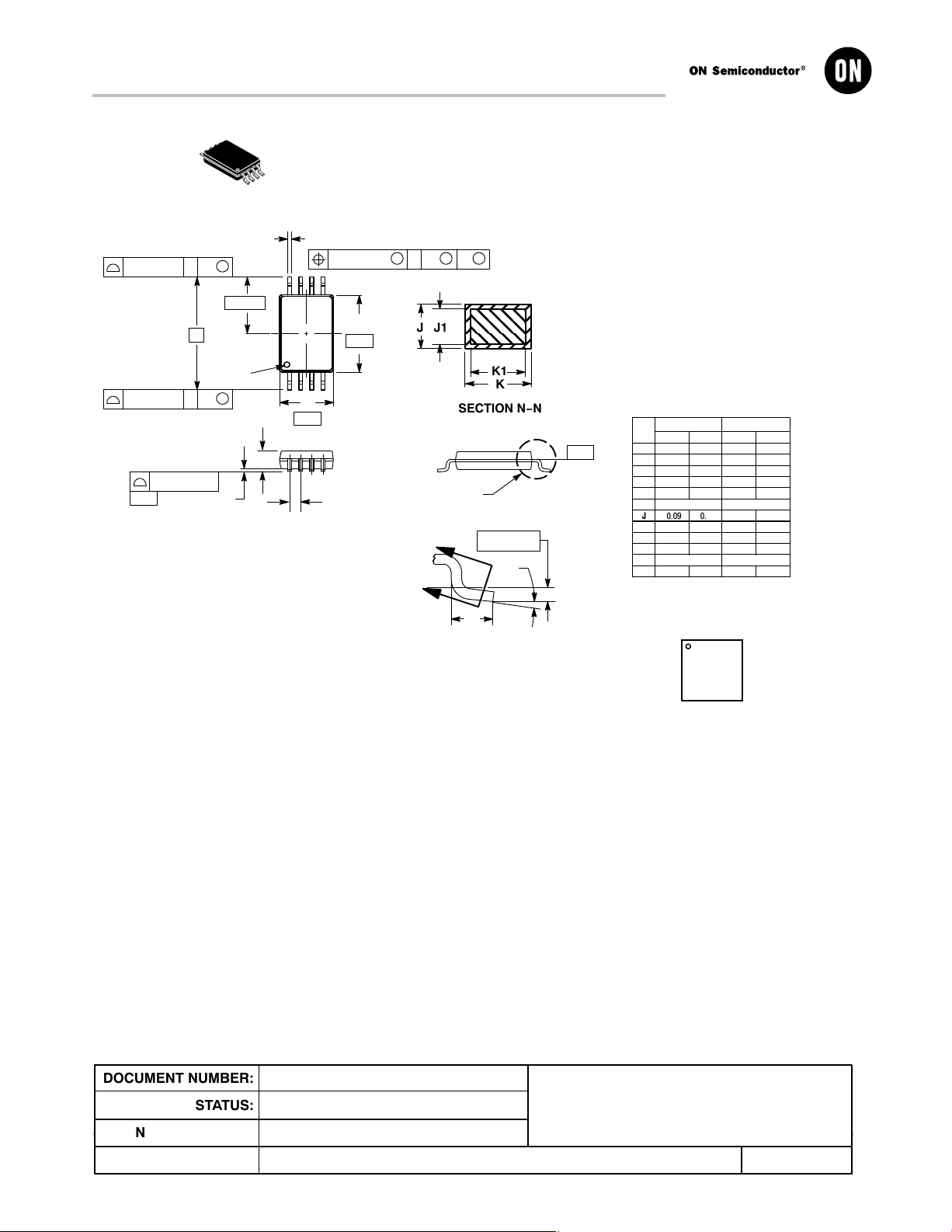
1
SCALE 2:1
0.10 (0.004)
SEATING
−T−
PLANE
S
U0.15 (0.006) T
2X L/2
L
PIN 1
IDENT.
S
U0.15 (0.006) T
C
D
SOLDERING FOOTPRINT
1
14X REFK
0.10 (0.004) V
14
1
M
8
7
A
−V−
G
7.06
TSSOP−14 WB
U
T
B
N
−U−
J
H
CASE 948G
ISSUE C
S
S
N
F
DETAIL E
J1
SECTION N−N
DETAIL E
0.25 (0.010)
M
K
K1
DATE 17 FEB 2016
NOTES:
1. DIMENSIONING AND TOLERANCING PER
ANSI Y14.5M, 1982.
2. CONTROLLING DIMENSION: MILLIMETER.
3. DIMENSION A DOES NOT INCLUDE MOLD
FLASH, PROTRUSIONS OR GATE BURRS.
MOLD FLASH OR GATE BURRS SHALL NOT
EXCEED 0.15 (0.006) PER SIDE.
4. DIMENSION B DOES NOT INCLUDE
INTERLEAD FLASH OR PROTRUSION.
INTERLEAD FLASH OR PROTRUSION SHALL
NOT EXCEED 0.25 (0.010) PER SIDE.
5. DIMENSION K DOES NOT INCLUDE DAMBAR
PROTRUSION. ALLOWABLE DAMBAR
PROTRUSION SHALL BE 0.08 (0.003) TOTAL
IN EXCESS OF THE K DIMENSION AT
MAXIMUM MATERIAL CONDITION.
6. TERMINAL NUMBERS ARE SHOWN FOR
REFERENCE ONLY.
7. DIMENSION A AND B ARE TO BE
DETERMINED AT DATUM PLANE −W−.
INCHESMILLIMETERS
−W−
DIM MIN MAX MIN MAX
A 4.90 5.10 0.193 0.200
B 4.30 4.50 0.169 0.177
C −−− 1.20 −−− 0.047
D 0.05 0.15 0.002 0.006
F 0.50 0.75 0.020 0.030
G 0.65 BSC 0.026 BSC
H 0.50 0.60 0.020 0.024
J 0.09 0.20 0.004 0.008
J1 0.09 0.16 0.004 0.006
K 0.19 0.30 0.007 0.012
K1 0.19 0.25 0.007 0.010
L 6.40 BSC 0.252 BSC
M 0 8 0 8
____
GENERIC
MARKING DIAGRAM*
14
XXXX
XXXX
ALYWG
G
1
A = Assembly Location
L = Wafer Lot
Y = Year
0.65
PITCH
W = Work Week
G = Pb−Free Package
(Note: Microdot may be in either location)
*This information is generic. Please refer to
14X
0.36
DOCUMENT NUMBER:
DESCRIPTION:
ON Semiconductor and are trademarks of Semiconductor Components Industries, LLC dba ON Semiconductor or its subsidiaries in the United States and/or other countries.
ON Semiconductor reserves the right to make changes without further notice to any products herein. ON Semiconductor makes no warranty, representation or guarantee regarding
the suitability of its products for any particular purpose, nor does ON Semiconductor assume any liability arising out of the application or use of any product or circuit, and specifically
disclaims any and all liability, including without limitation special, consequential or incidental damages. ON Semiconductor does not convey any license under its patent rights nor the
rights of others.
© Semiconductor Components Industries, LLC, 2019
14X
1.26
98ASH70246A
TSSOP−14 WB
DIMENSIONS: MILLIMETERS
Electronic versions are uncontrolled except when accessed directly from the Document Repository.
Printed versions are uncontrolled except when stamped “CONTROLLED COPY” in red.
device data sheet for actual part marking.
Pb−Free indicator, “G” or microdot “ G”,
may or may not be present.
PAGE 1 OF 1
www.onsemi.com
Page 25
MECHANICAL CASE OUTLINE
PACKAGE DIMENSIONS
SCALE 2:1
TSSOP−8
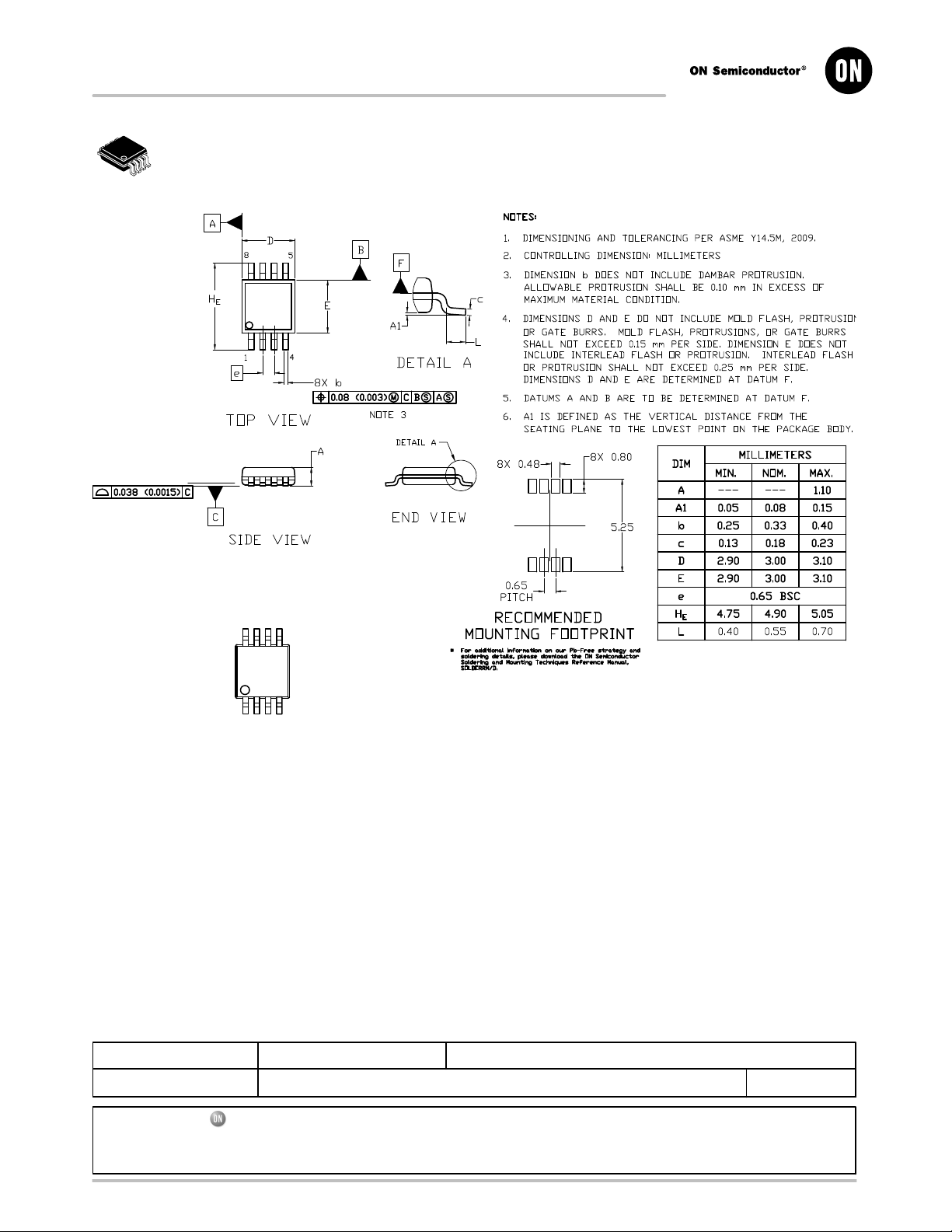
CASE 948S−01
ISSUE C
DATE 20 JUN 2008
0.076 (0.003)
−T−
SEATING
PLANE
8x REFK
U
T
JJ1
S
S
K1
K
SECTION N−N
S
U0.20 (0.008) T
2X L/2
85
L
PIN 1
IDENT
S
U0.20 (0.008) T
0.10 (0.004) V
−U−
1
4
A
M
B
−V−
C
D
G
DETAIL E
N
0.25 (0.010)
M
−W−
NOTES:
1. DIMENSIONING AND TOLERANCING PER ANSI
Y14.5M, 1982.
2. CONTROLLING DIMENSION: MILLIMETER.
3. DIMENSION A DOES NOT INCLUDE MOLD FLASH.
PROTRUSIONS OR GATE BURRS. MOLD FLASH
OR GATE BURRS SHALL NOT EXCEED 0.15
(0.006) PER SIDE.
4. DIMENSION B DOES NOT INCLUDE INTERLEAD
FLASH OR PROTRUSION. INTERLEAD FLASH OR
PROTRUSION SHALL NOT EXCEED 0.25 (0.010)
PER SIDE.
5. TERMINAL NUMBERS ARE SHOWN FOR
REFERENCE ONLY.
6. DIMENSION A AND B ARE TO BE DETERMINED
AT DATUM PLANE -W-.
DIM MIN MAX MIN MAX
A 2.90 3.10 0.114 0.122
B 4.30 4.50 0.169 0.177
C --- 1.10 --- 0.043
D 0.05 0.15 0.002 0.006
F 0.50 0.70 0.020 0.028
G 0.65 BSC 0.026 BSC
J 0.09 0.20 0.004 0.008
J1 0.09 0.16 0.004 0.006
K 0.19 0.30 0.007 0.012
K1 0.19 0.25 0.007 0.010
L 6.40 BSC 0.252 BSC
M 0 8 0 8
____
INCHESMILLIMETERS
N
GENERIC
F
DETAIL E
MARKING DIAGRAM*
XXX
YWW
A G
G
XXX = Specific Device Code
A = Assembly Location
Y = Year
WW = Work Week
G = Pb−Free Package
DOCUMENT NUMBER:
STATUS:
NEW STANDARD:
© Semiconductor Components Industries, LLC, 2002
October, 2002 − Rev. 0
DESCRIPTION:
98AON00697D
ON SEMICONDUCTOR STANDARD
TSSOP−8
http://onsemi.com
1
*This information is generic. Please refer to
device data sheet for actual part marking.
Pb−Free indicator, “G” or microdot “ G”,
may or may not be present.
Electronic versions are uncontrolled except when
accessed directly from the Document Repository. Printed
versions are uncontrolled except when stamped
“CONTROLLED COPY” in red.
Case Outline Number:
PAGE 1 OF 2
XXX
Page 26

DOCUMENT NUMBER:
98AON00697D
PAGE 2 OF 2
ISSUE REVISION DATE
O RELEASED FOR PRODUCTION. 18 APR 2000
A ADDED MARKING DIAGRAM INFORMATION. REQ. BY V. BASS. 13 JAN 2006
B CORRECTED MARKING DIAGRAM PIN 1 LOCATION AND MARKING. REQ. BY C.
13 MAR 2006
REBELLO.
C REMOVED EXPOSED PAD VIEW AND DIMENSIONS P AND P1. CORRECTED
20 JUN 2008
MARKING INFORMATION. REQ. BY C. REBELLO.
ON Semiconductor and are registered trademarks of Semiconductor Components Industries, LLC (SCILLC). SCILLC reserves the right to make changes without further notice
to any products herein. SCILLC makes no warranty, representation or guarantee regarding the suitability of its products for any particular purpose, nor does SCILLC assume any liability
arising out of the application or use of any product or circuit, and specifically disclaims any and all liability, including without limitation special, consequential or incidental damages.
“Typical” parameters which may be provided in SCILLC data sheets and/or specifications can and do vary in different applications and actual performance may vary over time. All
operating parameters, including “Typicals” must be validated for each customer application by customer’s technical experts. SCILLC does not convey any license under its patent rights
nor the rights of others. SCILLC products are not designed, intended, or authorized for use as components in systems intended for surgical implant into the body, or other applications
intended to support or sustain life, or for any other application in which the failure of the SCILLC product could create a situation where personal injury or death may occur. Should
Buyer purchase or use SCILLC products for any such unintended or unauthorized application, Buyer shall indemnify and hold SCILLC and its officers, employees, subsidiaries, affiliates,
and distributors harmless against all claims, costs, damages, and expenses, and reasonable attorney fees arising out of, directly or indirectly, any claim of personal injury or death
associated with such unintended or unauthorized use, even if such claim alleges that SCILLC was negligent regarding the design or manufacture of the part. SCILLC is an Equal
Opportunity/Affirmative Action Employer. This literature is subject to all applicable copyright laws and is not for resale in any manner.
© Semiconductor Components Industries, LLC, 2008
Case Outline Number:
June, 2008 − Rev. 01C
948S
Page 27

ON Semiconductor and are trademarks of Semiconductor Components Industries, LLC dba ON Semiconductor or its subsidiaries in the United States and/or other countries.
ON Semiconductor owns the rights to a number of patents, trademarks, copyrights, trade secrets, and other intellectual property. A listing of ON Semiconductor’s product/patent
coverage may be accessed at www.onsemi.com/site/pdf/Patent−Marking.pdf
ON Semiconductor makes no warranty, representation or guarantee regarding the suitability of its products for any particular purpose, nor does ON Semiconductor assume any liability
arising out of the application or use of any product or circuit, and specifically disclaims any and all liability, including without limitation special, consequential or incidental damages.
Buyer is responsible for its products and applications using ON Semiconductor products, including compliance with all laws, regulations and safety requirements or standards,
regardless of any support or applications information provided by ON Semiconductor. “Typical” parameters which may be provided in ON Semiconductor data sheets and/or
specifications can and do vary in different applications and actual performance may vary over time. All operating parameters, including “Typicals” must be validated for each customer
application by customer’s technical experts. ON Semiconductor does not convey any license under its patent rights nor the rights of others. ON Semiconductor products are not
designed, intended, or authorized for use as a critical component in life support systems or any FDA Class 3 medical devices or medical devices with a same or similar classification
in a foreign jurisdiction or any devices intended for implantation in the human body. Should Buyer purchase or use ON Semiconductor products for any such unintended or unauthorized
application, Buyer shall indemnify and hold ON Semiconductor and its officers, employees, subsidiaries, affiliates, and distributors harmless against all claims, costs, damages, and
expenses, and reasonable attorney fees arising out of, directly or indirectly, any claim of personal injury or death associated with such unintended or unauthorized use, even if such
claim alleges that ON Semiconductor was negligent regarding the design or manufacture of the part. ON Semiconductor is an Equal Opportunity/Affirmative Action Employer. This
literature is subject to all applicable copyright laws and is not for resale in any manner.
. ON Semiconductor reserves the right to make changes without further notice to any products herein.
PUBLICATION ORDERING INFORMATION
LITERATURE FULFILLMENT:
Email Requests to: orderlit@onsemi.com
ON Semiconductor Website: www.onsemi.com
TECHNICAL SUPPORT
North American Technical Support:
Voice Mail: 1 800−282−9855 Toll Free USA/Canada
Phone: 011 421 33 790 2910
Europe, Middle East and Africa Technical Support:
Phone: 00421 33 790 2910
For additional information, please contact your local Sales Representative
◊
www.onsemi.com
1
 Loading...