

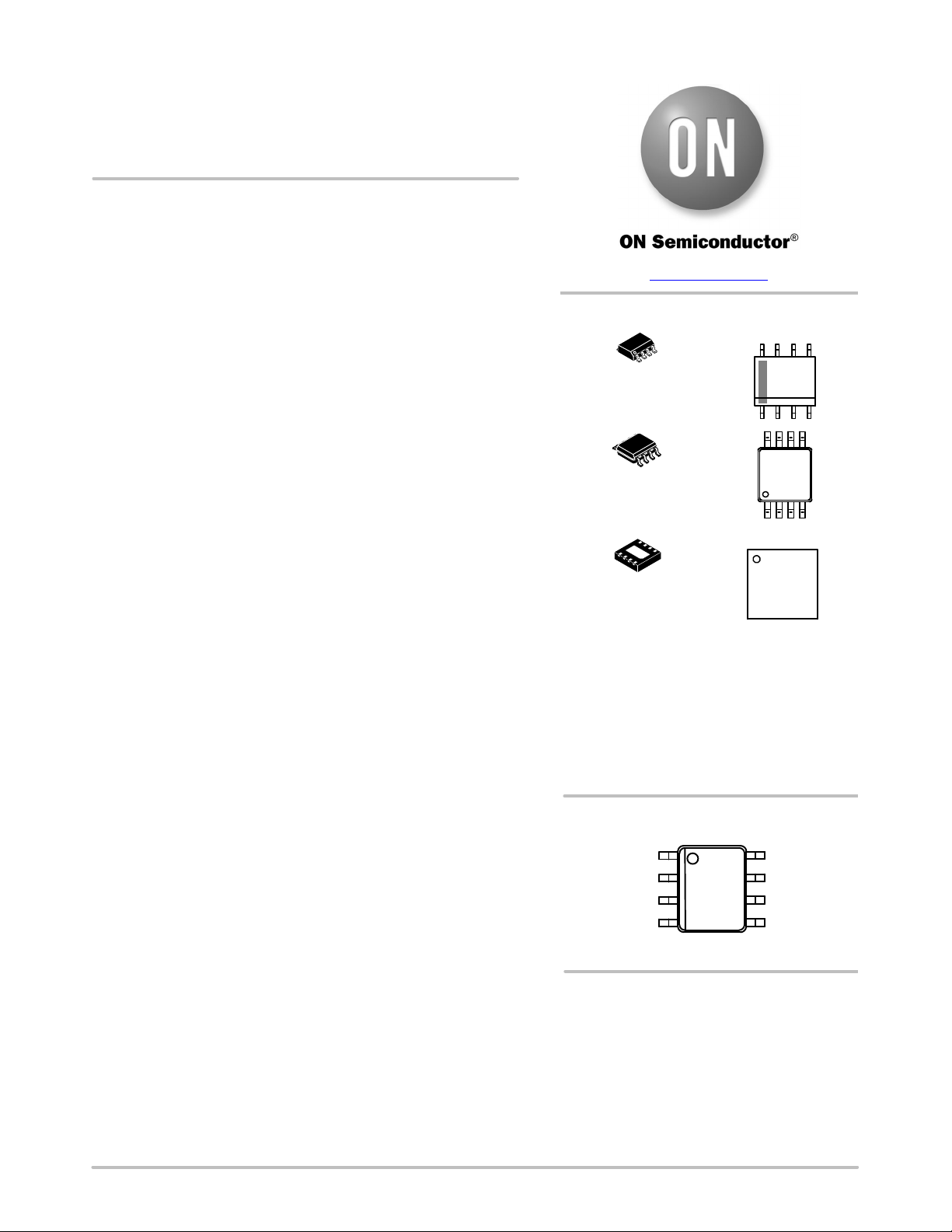
Page 1
Dual 5 A High Speed
Low-Side MOSFET Drivers
with Enable
NCP81071
NCP81071 is a high speed dual low−side MOSFETs driver. It is
capable of providing large peak currents into capacitive loads. This
driver can deliver 5 A peak current at the Miller plateau region to help
reduce the Miller effect during MOSFETs switching transition. This
driver also provides enable functions to give users better control
capability in different applications. ENA and ENB are implemented
on pin 1 and pin 8 which were previously unused in the industry
standard pin−out. They are internally pulled up to driver’s input
voltage for active high logic and can be left open for standard
operations. This part is available in MSOP8−EP package, SOIC8
package and WDFN8 3 mm x 3 mm package.
Features
• High Current Drive Capability ±5 A
• TTL/CMOS Compatible Inputs Independent of Supply Voltage
• Industry Standard Pin−out
• High Reverse Current Capability (6 A) Peak
• Enable Functions for Each Driver
• 8 ns Typical Rise and 8 ns Typical Fall Times with 1.8 nF Load
• Typical Propagation Delay Times of 20 ns with Input Falling and
20ns with Input Rising
• Input Voltage from 4.5 V to 20 V
• Dual Outputs can be Paralleled for Higher Drive Current
• These Devices are Pb−Free, Halogen Free/BFR Free and are RoHS
Compliant
Applications
• Server Power
• Telecommunication, Datacenter Power
• Synchronous Rectifier
• Switch Mode Power Supply
• DC/DC Converter
• Power Factor Correction
• Motor Drive
• Renewable Energy, Solar Inverter
www.onsemi.com
MARKING
DIAGRAMS
8
SOIC−8
D SUFFIX
CASE 751
MSOP−8
Z SUFFIX
CASE 846AM
1
WDFN8
MN SUFFIX
CASE 511CD
XX = Specific Device Code
A = Assembly Location
L = Wafer Lot
Y = Year
W = Work Week
M = Date Code
G = Pb−Free Package
(Note: Microdot may be in either location)
PIN CONNECTIONS
1
ENA
INA
GND
INB
(Top View)
XXXX
ALYW
G
1
XXXX
AYW
G
1
XX MG
G
8
ENB
OUTA
VDD
OUTB
© Semiconductor Components Industries, LLC, 2016
March, 2021 − Rev. 4
ORDERING INFORMATION
See detailed ordering and shipping information in the package
dimensions section on page 11 of this data sheet.
1 Publication Order Number:
NCP81071/D
Page 2
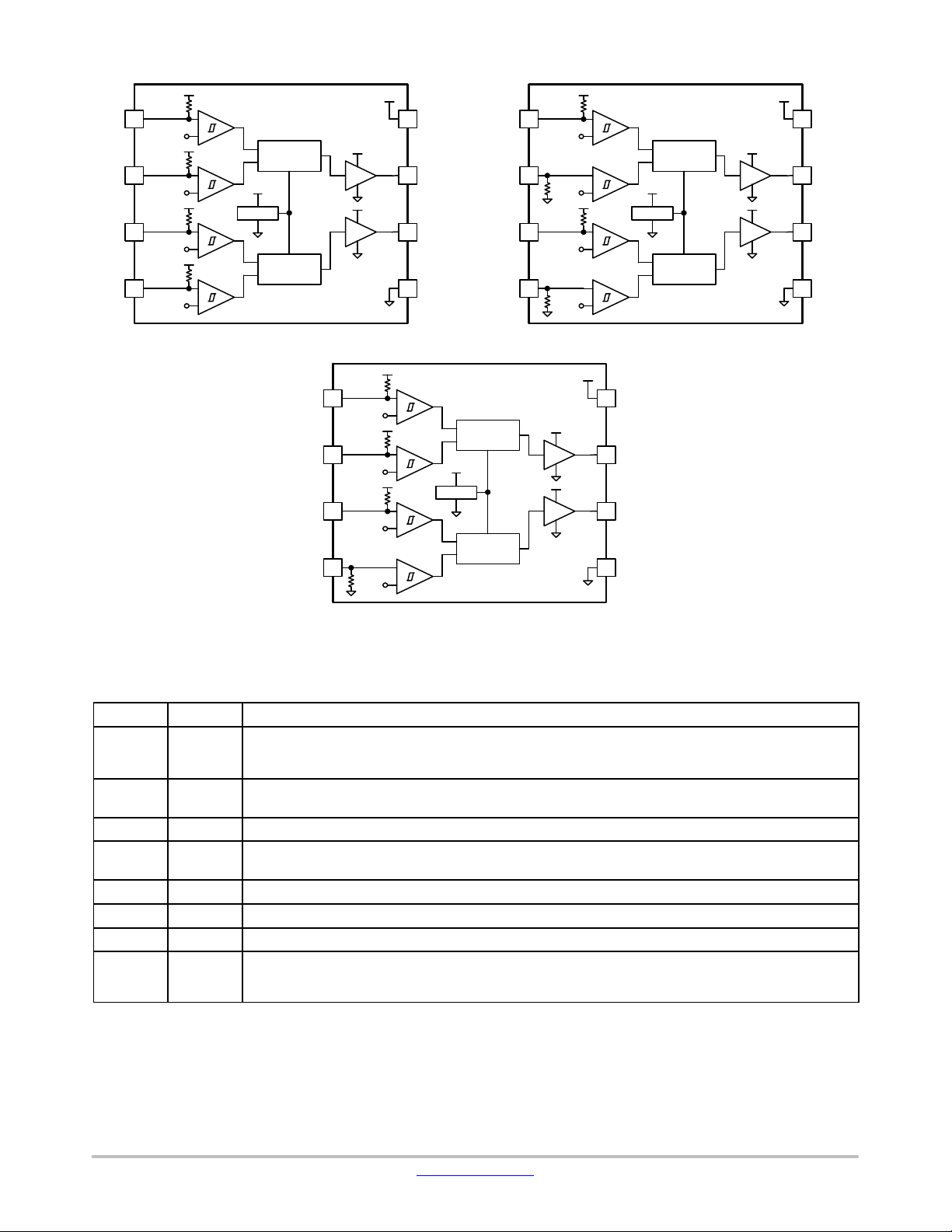
NCP81071
ENA
INA
ENB
INB
Ref
Ref
Ref
Ref
VDD
VDD
Ref
Ref
Ref
Ref
VDD
VDD
VDD
VDD
VDD
OUTA
OUTB
GND
UVLO
ENA
INA
ENB
INB
Logic
A Channel
VDD
Logic
B Channel
VDD
Ref
Ref
VDD
Ref
Ref
VDD
VDD
VDD
OUTA
VDD
OUTB
GND
VDD
VDD
VDD
VDD
NCP81071A NCP81071B
A Channel
VDD
UVLO
B Channel
Logic
Logic
ENA
INA
ENB
INB
A Channel
VDD
UVLO
B Channel
Logic
Logic
VDD
VDD
VDD
OUTA
VDD
OUTB
GND
NCP81071C
Figure 1. NCP81071 Block Diagram
Table 1. PIN DESCRIPTION
Pin No. Symbol Description
1 ENA Enable input for the driver channel A with logic compatible threshold and hysteresis. This pin is used to en-
2 INA Input of driver channel A which has logic compatible threshold and hysteresis. If not used, this pin should be
3 GND Common ground. This ground should be connected very closely to the source of the power MOSFET.
4 INB Input of driver channel B which has logic compatible threshold and hysteresis. If not used, this pin should be
5 OUTB Output of driver channel B. The driver is able to provide 5 A drive current to the gate of the power MOSFET.
6 VDD Supply voltage. Use this pin to connect the input power for the driver device.
7 OUTA Output of driver channel A. The driver is able to provide 5 A drive current to the gate of the power MOSFET.
8 ENB Enable input for the driver channel B with logic compatible threshold and hysteresis. This pin is used to en-
able and disable the driver output. It is internally pulled up to VDD with a 200 kW resistor for active high operation. The output of the pin when the device is disabled will be always low.
connected to either VDD or GND. It should not be left unconnected.
connected to either VDD or GND. It should not be left unconnected.
able and disable the driver output. It is internally pulled up to VDD with a 200 kW resistor for active high operation. The output of the pin when the device is disabled will be always low.
www.onsemi.com
2
Page 3
NCP81071
TYPICAL APPLICATION CIRCUIT
ENA
INA
GND
INB
NCP81071
1
2
3
4
8
7
6
5
ENB
OUTA
VDD
OUTB
Table 2. ABSOLUTE MAXIMUM RATINGS
Value
Min Max
Supply Voltage VDD −0.3 24 V
Output Current (DC) Iout_dc 0.3 A
Reverse Current (Pulse< 1 ms)
Output Current (Pulse < 0.5 ms)
Input Voltage INA, INB −6.0 VDD+0.3
Enable Voltage ENA, ENB −0.3 VDD+0.3
Output Voltage OUTA, OUTB −0.3 VDD+0.3 V
Output Voltage (Pulse < 0.5 ms)
Junction Operation Temperature T
Storage Temperature T
Electrostatic Discharge
OUTA OUTB Latch−up Protection 500 mA
Stresses exceeding those listed in the Maximum Ratings table may damage the device. If any of these limits are exceeded, device functionality
should not be assumed, damage may occur and reliability may be affected.
Iout_pulse 6.0 A
OUTA, OUTB −3.0 VDD+3.0 V
J
stg
Human body model, HBM 4000
Charge device model, CDM 1000
−40 150
−65 160
6.0 A
Unit
V
°C
V
Table 3. RECOMMENDED OPERATING CONDITIONS
Parameter Rating Unit
VDD supply Voltage 4.5 to 20 V
INA, INB input voltage −5.0 to VDD V
ENA, ENB input voltage 0 to VDD V
Junction Temperature Range −40 to +140 °C
Functional operation above the stresses listed in the Recommended Operating Ranges is not implied. Extended exposure to stresses beyond
the Recommended Operating Ranges limits may affect device reliability.
Table 4. THERMAL INFORMATION
Package
SOIC−8 115 50
MSOP−8 EP 39 4.7 11
WDFN8 3x3 39 4.7
1. YJT: approximate thermal impedance, junction−to−case top.
qJA (5C/W) qJC (5C/W) YJT (5C/W) (Note 1)
www.onsemi.com
3
Page 4
NCP81071
Table 5. INPUT/OUTPUT TABLE
NCP81071A NCP81071B NCP81071C
ENA ENB INA INB
H H L L H H L L H L
H H L H H L L H H H
H H H L L H H L L L
H H H H L L H H L H
L L Any Any L L L L L L
Any Any x (Note 2) x (Note 2) L L L L L L
x (Note 2) x (Note 2) L L H H L L H L
x (Note 2) x (Note 2) L H H L L H H H
x (Note 2) x (Note 2) H L L H H L L L
x (Note 2) x (Note 2) H H L L H H L H
2. Floating condition, internal resistive pull up or pull down configures output condition
OUTA OUTB OUTA OUTB OUTA OUTB
PRODUCT MATRIX
NCP81071A NCP81071B NCP81071C
www.onsemi.com
4
Page 5
NCP81071
Table 6. ELECTRICAL CHARACTERISTICS
(Typical values: VDD =12 V, 1 mF from VDD to GND, TA = TJ = −40°C to 140°C, typical at T
Parameter
Symbol Test Conditions Min Typ Max Units
SUPPLY VOLTAGE
VDD Under Voltage Lockout (rising) V
VDD Under Voltage Lockout
(hysteresis)
Operating Current (no switching) I
V
CCR
CCH
DD
VDD rising 3.5 4.0 4.5 V
INA = 0, INB = 5 V, ENA = ENB = 0
INA = 5 V, INB = 0, ENA = ENB = 0
INA = 0, INB = 5 V, ENA = ENB = 5 V
INA = 5 V, INB = 0, ENA = ENB = 5 V
VDD Under Voltage Lockout to Output
VDD rising 10
Delay (Note 3)
INPUTS
High Threshold
Low Threshold V
V
thH
thL
Input rising from logic low 1.8 2.0 2.2 V
Input falling from logic high 0.8 1.0 1.2 V
INA, INB Pull−Up Resistance OUTA = OUTB = Inverter Configuration 200
INA, INB Pull−Down Resistance OUTA = OUTB = Buffer Configuration 200
OUTPUTS
Output Resistance High
Output Resistance Low R
Peak Source Current (Note 4) I
Miller Plateau Source Current (Note 4) I
Source
Source
Peak Sink Current (Note 4) I
Miller Plateau Sink Current (Note 4) I
R
Sink
Sink
OH
OL
IOUT = −10 mA 0.8 2
IOUT = +10 mA 0.8 2
OUTA/OUTB = GND
200 ns Pulse
OUTA/OUTB = 5.0 V
200 ns Pulse
OUTA/OUTB = VDD
200 ns Pulse
OUTA/OUTB = 5.0 V
200 ns Pulse
ENABLE
High−Level Input Voltage
Low−Level Input Voltage V
V
IN_H
IN_L
Low to High Transition 1.8 2.0 2.2 V
High to Low Transition 0.8 1.0 1.2 V
ENA, ENB pull−up resistance 200
Propagation Delay Time (EN to OUT)
(Notes 3, 5)
Propagation Delay Time (EN to OUT)
(Notes 3, 5)
t
d3
t
d4
C
= 1.8 nF 16 20 29 ns
Load
C
= 1.8 nF 16 20 29 ns
Load
SWITCHING CHARACTERISTICS
Propagation Delay Time Low to High,
IN Rising (IN to OUT) (Notes 3, 5)
Propagation Delay Time High to Low,
IN Falling (IN to OUT) (Notes 3, 5)
Rise Time (Note 5) t
Fall Time (Note 5) t
Delay Matching between 2 Channels
(Note 6)
t
d1
t
d2
r
f
t
m
C
= 1.8 nF 16 20 29 ns
Load
C
= 1.8 nF 16 20 29 ns
Load
C
= 1.8 nF 8 15 ns
Load
C
= 1.8 nF 8 15 ns
Load
INA = INB, OUTA and OUTB at 50%
Transition Point
Product parametric performance is indicated in the Electrical Characteristics for the listed test conditions, unless otherwise noted. Product
performance may not be indicated by the Electrical Characteristics if operated under different conditions.
3. Guaranteed by design.
4. Not production tested, guaranteed by design and statistical analysis.
5. See timing diagrams in Figure 2, Figure 3, Figure 4 and Figure 5.
6. Guaranteed by characterization.
= 25°C, unless otherwise specified)
AMB
400 mV
1.4 3 mA
5 A
4.5 A
5 A
3.5 A
1 4 ns
ms
kW
kW
W
W
kW
www.onsemi.com
5
Page 6

NCP81071
Input
Enable
Output
Input
Enable
2 V
1 V
2 V
1 V
90%
10%
t
d3
Figure 2. Enable Function for
Non−inverting Input Driver Operation
2 V
1 V
2 V
1 V
2 V
Input
1 V
2 V
Enable
1 V
90%
Output
10%
t
d4
t
d3
t
d4
Figure 3. Enable Function for Inverting
Input Driver Operation
2 V
Input
1 V
2 V
Enable
1 V
Output
90%
10%
t
t
d1
r
t
t
d2
f
Output
90%
10%
t
d1
t
d2
Figure 4. Non−inverting Input Driver Operation Figure 5. Inverting Input Driver Operation
www.onsemi.com
6
Page 7

NCP81071
TYPICAL CHARACTERISTICS
100
90
80
70
60
50
40
30
SUPPLY CURRENT (mA)
20
10
0
VDD = 4.5 V
Figure 6. Supply Current vs. Switching
270
240
210
180
150
120
90
60
SUPPLY CURRENT (mA)
30
0
Figure 8. Supply Current vs. Switching
270
240
210
180
150
120
SUPPLY CURRENT (mA)
VDD = 18 V
90
60
30
0
Figure 10. Supply Current vs. Switching
180
10 nF
4.7 nF
2.2 nF
1 nF
470 pF
600 1600 1800
FREQUENCY (kHz) FREQUENCY (kHz)
20001400120010008004002000
160
140
120
100
80
60
40
SUPPLY CURRENT (mA)
20
0
VDD = 8.0 V
Figure 7. Supply Current vs. Switching
Frequency (V
VDD = 12 V
FREQUENCY (kHz) FREQUENCY (kHz)
= 4.5 V)
DD
12501000750 20005002500
10 nF
4.7 nF
2.2 nF
1 nF
470 pF
1500 1750
270
240
210
180
150
120
SUPPLY CURRENT (mA)
VDD = 15 V
90
60
30
0
Frequency (VDD = 8 V)
10 nF
Figure 9. Supply Current vs. Switching
Frequency (V
10 nF
4.7 nF
FREQUENCY (kHz) SUPPLY VOLTAGE (V)
= 12 V)
DD
12501000750 20005002500
2.2 nF
1 nF
470 pF
1500 1750
120
100
80
60
40
SUPPLY CURRENT (mA)
20
0
C
LOAD
Frequency (VDD = 15 V)
= 2.2 nF
50 kHz
Figure 11. Supply Current vs. Supply Voltage
Frequency (V
= 18 V)
DD
(C
LOAD
12501000750 20005002500
12501000750 20005002500
100 kHz
= 2.2 nF)
10 nF
4.7 nF
2.2 nF
1 nF
470 pF
1500 1750
4.7 nF
2.2 nF
1 nF
470 pF
1500 1750
2 MHz
1 MHz
500 kHz
200 kHz
1816141210864
20
www.onsemi.com
7
Page 8

NCP81071
TYPICAL CHARACTERISTICS
160
140
C
LOAD
120
100
80
60
40
SUPPLY CURRENT (mA)
20
0
Figure 12. Supply Current vs. Supply Voltage
2.0
1.8
1.6
1.4
1.2
1.0
0.8
0.6
SUPPLY CURRENT (mA)
0.4
0.2
0
Figure 14. Supply Current vs. Supply Voltage
2.0
1.8
1.6
1.4
1.2
1.0
0.8
0.6
SUPPLY CURRENT (mA)
0.4
0.2
0
Input = GND
1 MHz
100 kHz
2 MHz
500 kHz
200 kHz
1816141210864
20
= 4.7 nF
50 kHz
SUPPLY VOLTAGE (V) SUPPLY VOLTAGE (V)
Figure 13. Supply Current vs. Supply Voltage
(C
Input = GND
SUPPLY VOLTAGE (V)
LOAD
= 4.7 nF)
Input = V
DD
(NCP81071A)
2.0
1.8
1.6
1.4
1.2
1.0
0.8
0.6
SUPPLY CURRENT (mA)
0.4
0.2
20
1816141210864
0
Input = GND
SUPPLY VOLTAGE (V)
Figure 15. Supply Current vs. Supply Voltage
(NCP81071B)
(NCP81071C)
Input = V
Input = V
DD
DD
1816141210864
20
20
1816141210864
12
10
8
VDD = 20 V
6
4
, RISE TIME (ns)
t
r
VDD = 10 V
2
0
Figure 16. Rise Time vs. Temperature Figure 17. Fall Time vs. Temperature
VDD = 15 V
VDD = 5 V
40 140
TEMPERATURE (°C)
12
10
, FALL TIME (ns)
f
t
1201008060200−20−40
www.onsemi.com
8
8
VDD = 20 V
6
4
VDD = 10 V
2
0
VDD = 15 V
VDD = 5 V
40 140
TEMPERATURE (°C)
1201008060200−20−40
Page 9

NCP81071
TYPICAL CHARACTERISTICS
30
25
20
15
10
, DELAY TIME (ns)
d1
t
5
0
Figure 18. Propagation Delay td1 vs. Supply
30
25
20
15
10
, FALL TIME (ns)
f
t
5
0
Figure 20. Fall Time tf vs. Supply Voltage Figure 21. Rise Time tr vs. Supply Voltage
30
25
20
15
10 nF
4.7 nF
2.2 nF
1.0 nF
470 pF
20
1816141210864
VDD, SUPPLY VOLTAGE (V) VDD, SUPPLY VOLTAGE (V)
10
, DELAY TIME (ns)
d2
t
5
0
Figure 19. Propagation Delay td2 vs. Supply
Voltage
35
30
10 nF
4.7 nF
1.0 nF
VDD, SUPPLY VOLTAGE (V) VDD, SUPPLY VOLTAGE (V)
2.2 nF
470 pF
20
1816141210864
25
20
15
, RISE TIME (ns)
r
t
10
5
0
Voltage
1.0 nF
10 nF
4.7 nF
2.2 nF
1.0 nF
470 pF
1816141210864
10 nF
4.7 nF
2.2 nF
470 pF
1816141210864
20
20
VDD
Output
Figure 22. Output Behavior vs. Supply Voltage
NCP81071A (Inverting) 10 nF between Output
and GND, INA = GND, ENA = VDD
www.onsemi.com
VDD
Output
Figure 23. Output Behavior vs. Supply Voltage
NCP81071A (Inverting) 10 nF between Output
and GND, INA = GND, ENA = VDD
9
Page 10

NCP81071
TYPICAL CHARACTERISTICS
VDD
Output
Figure 24. Output Behavior vs. Supply Voltage
NCP81071A (Inverting) 10 nF between Output
and GND, INA = VDD, ENA = VDD
VDD
Output
VDD
Output
Figure 25. Output Behavior vs. Supply Voltage
NCP81071A (Inverting) 10 nF between Output
and GND, INA = VDD, ENA = VDD
VDD
Output
Figure 26. Output Behavior vs. Supply Voltage
NCP81071B (Non−Inverting) 10 nF between
Output and GND, INA = VDD, ENA = VDD
VDD
Output
Figure 28. Output Behavior vs. Supply Voltage
NCP81071B (Non−Inverting) 10 nF between
Output and GND, INA = GND, ENA = VDD
Figure 27. Output Behavior vs. Supply Voltage
NCP81071B (Non−Inverting) 10 nF between
Output and GND, INA = VDD, ENA = VDD
VDD
Output
Figure 29. Output Behavior vs. Supply Voltage
NCP81071B (Non−Inverting) 10 nF between
Output and GND, INA = GND, ENA = VDD
www.onsemi.com
10
Page 11

NCP81071
LAYOUT GUIDELINES
The switching performance of NCP81071 highly depends
on the design of PCB board. The following layout design
guidelines are recommended when designing boards using
these high speed drivers.
Place the driver as close as possible to the driven
MOSFET.
Place the bypass capacitor between VDD and GND as
close as possible to the driver to improve the noise filtering.
It is preferred to use low inductance components such as
chip capacitor and chip resistor. If vias are used, connect
several paralleled vias to reduce the inductance of the vias.
Minimize the turn-on/sourcing current and
turn-off/sinking current paths in order to minimize stray
inductance. Otherwise high di/dt established in these loops
with stray inductance can induce significant voltage spikes
on the output of the driver and MOSFET Gate terminal.
Keep power loops as short as possible by paralleling the
source and return traces (flux cancellation).
Keep low level signal lines away from high level power
lines with a lot of switching noise.
Place a ground plane for better noise shielding. Beside
noise shielding, ground plane is also useful for heat
dissipation.
NCP81071 DFN and MSOP package have thermal pad
for: 1) quiet GND for all the driver circuits; 2) heat sink for
the driver. This pad must be connected to a ground plane and
no switching currents from the driven MOSFET should pass
through the ground plane under the driver. To maximize the
heatsinking capability, it is recommended several ground
layers are added to connect to the ground plane and thermal
pad. A via array within the area of package can conduct the
heat from the package to the ground layers and the whole
PCB board. The number of vias and the size of ground plane
are determined by the power dissipation of NCP81071
(VDD voltage, switching frequency and load condition), the
air flow condition and its maximum junction temperature.
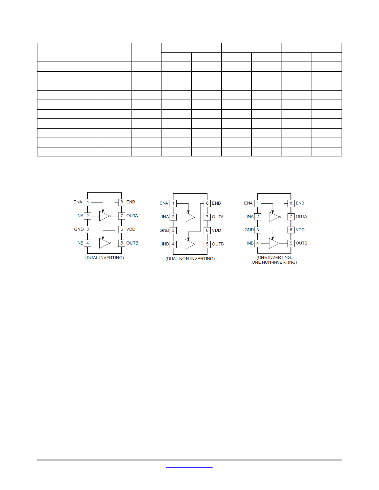
ORDERING INFORMATION
Part Number Output Configuration Temperature Range (5C) Package Type Shipping
NCP81071ADR2G dual inverting
NCP81071BDR2G dual non inverting
NCP81071CDR2G One inverting
NCP81071AZR2G dual inverting
NCP81071BZR2G dual non inverting
NCP81071CZR2G One inverting
NCP81071AMNTXG dual inverting
NCP81071BMNTXG dual non inverting
NCP81071CMNTXG One inverting
†For information on tape and reel specifications, including part orientation and tape sizes, please refer to our Tape and Reel Packaging
Specifications Brochure, BRD8011/D.
one non inverting
−40 to +140
one non inverting
one non inverting
www.onsemi.com
11
SOIC−8
(Pb−Free)
MSOP8 EP
(Pb−Free)
WDFN8
(Pb−Free)
2500 / Tape & Reel
3000 / Tape & Reel
3000 / Tape & Reel
†
Page 12

MECHANICAL CASE OUTLINE
PACKAGE DIMENSIONS
1
SCALE 2:1
WDFN8 3x3, 0.65P
CASE 511CD
ISSUE O
DATE 29 APR 2014
PIN ONE
REFERENCE
2X
2X
NOTE 4
DETAIL A
D
C0.10
C0.10
TOP VIEW
C0.05
C0.05
SIDE VIEW
D2
1
K
8
e/2
e
BOTTOM VIEW
RECOMMENDED
SOLDERING FOOTPRINT*
PACKAGE
OUTLINE
2.31
DETAIL B
A3
4
5
A1
8X
A
8X
E2
b
0.10 C
0.05 C
L
B
E
A
C
8X
0.63
L1
SEATING
PLANE
A
BB
NOTE 3
L
DETAIL A
ALTERNATE
CONSTRUCTIONS
MOLD CMPDEXPOSED Cu
DETAIL B
ALTERNATE
CONSTRUCTIONS
NOTES:
L
1. DIMENSIONING AND TOLERANCING PER
ASME Y14.5M, 1994.
2. CONTROLLING DIMENSION: MILLIMETERS.
3. DIMENSION b APPLIES TO PLATED
TERMINAL AND IS MEASURED BETWEEN
0.15 AND 0.30 MM FROM TERMINAL TIP.
4. COPLANARITY APPLIES TO THE EXPOSED
PAD AS WELL AS THE TERMINALS.
MILLIMETERS
DIM MIN MAX
A3
A1
A 0.70 0.80
A1 0.00 0.05
A3 0.20 REF
b 0.25 0.35
D 3.00 BSC
D2 2.05 2.25
E 3.00 BSC
E2 1.10 1.30
e 0.65 BSC
K
0.20 −−−
L 0.30 0.50
L1 0.00 0.15
GENERIC
MARKING DIAGRAM*
XXXXX
XXXXX
ALYWG
G
A = Assembly Location
L = Wafer Lot
Y = Year
W = Work Week
G = Pb−Free Package
(Note: Microdot may be in either location)
*This information is generic. Please refer to
device data sheet for actual part marking.
Pb−Free indicator, “G” or microdot “ G”,
may or may not be present.
8X
0.40
3.30
1.36
0.65
PITCH
1
DIMENSIONS: MILLIMETERS
*For additional information on our Pb−Free strategy and soldering
details, please download the ON Semiconductor Soldering and
Mounting Techniques Reference Manual, SOLDERRM/D.
DOCUMENT NUMBER:
DESCRIPTION:
ON Semiconductor and are trademarks of Semiconductor Components Industries, LLC dba ON Semiconductor or its subsidiaries in the United States and/or other countries.
ON Semiconductor reserves the right to make changes without further notice to any products herein. ON Semiconductor makes no warranty, representation or guarantee regarding
the suitability of its products for any particular purpose, nor does ON Semiconductor assume any liability arising out of the application or use of any product or circuit, and specifically
disclaims any and all liability, including without limitation special, consequential or incidental damages. ON Semiconductor does not convey any license under its patent rights nor the
rights of others.
© Semiconductor Components Industries, LLC, 2019
98AON84944F
WDFN8, 3X3, 0.65P
Electronic versions are uncontrolled except when accessed directly from the Document Repository.
Printed versions are uncontrolled except when stamped “CONTROLLED COPY” in red.
PAGE 1 OF 1
www.onsemi.com
Page 13

MECHANICAL CASE OUTLINE
PACKAGE DIMENSIONS
8
1
SCALE 1:1
B
−Y−
−Z−
−X−
A
58
1
4
G
H
D
0.25 (0.010) Z
M
SOLDERING FOOTPRINT*
7.0
0.275
S
Y
0.25 (0.010)
C
SEATING
PLANE
SXS
0.060
0.155
0.10 (0.004)
1.52
4.0
CASE 751−07
M
M
Y
N
SOIC−8 NB
ISSUE AK
K
X 45
_
M
J
MARKING DIAGRAM*
8
XXXXX
ALYWX
1
XXXXX = Specific Device Code
A = Assembly Location
L = Wafer Lot
Y = Year
W = Work Week
G = Pb−Free Package
8
XXXXX
ALYWX
G
1
IC
IC
(Pb−Free)
DATE 16 FEB 2011
NOTES:
1. DIMENSIONING AND TOLERANCING PER
ANSI Y14.5M, 1982.
2. CONTROLLING DIMENSION: MILLIMETER.
3. DIMENSION A AND B DO NOT INCLUDE
MOLD PROTRUSION.
4. MAXIMUM MOLD PROTRUSION 0.15 (0.006)
PER SIDE.
5. DIMENSION D DOES NOT INCLUDE DAMBAR
PROTRUSION. ALLOWABLE DAMBAR
PROTRUSION SHALL BE 0.127 (0.005) TOTAL
IN EXCESS OF THE D DIMENSION AT
MAXIMUM MATERIAL CONDITION.
6. 751−01 THRU 751−06 ARE OBSOLETE. NEW
STANDARD IS 751−07.
MILLIMETERS
DIMAMIN MAX MIN MAX
4.80 5.00 0.189 0.197
B 3.80 4.00 0.150 0.157
C 1.35 1.75 0.053 0.069
D 0.33 0.51 0.013 0.020
G 1.27 BSC 0.050 BSC
H 0.10 0.25 0.004 0.010
J 0.19 0.25 0.007 0.010
K 0.40 1.27 0.016 0.050
M 0 8 0 8
____
N 0.25 0.50 0.010 0.020
S 5.80 6.20 0.228 0.244
INCHES
GENERIC
8
XXXXXX
AYWW
1
Discrete
XXXXXX = Specific Device Code
A = Assembly Location
Y = Year
WW = Work Week
G = Pb−Free Package
8
XXXXXX
AYWW
1
Discrete
(Pb−Free)
G
0.6
0.024
1.270
0.050
SCALE 6:1
ǒ
inches
mm
Ǔ
*This information is generic. Please refer to
device data sheet for actual part marking.
Pb−Free indicator, “G” or microdot “G”, may
or may not be present. Some products may
not follow the Generic Marking.
*For additional information on our Pb−Free strategy and soldering
details, please download the ON Semiconductor Soldering and
Mounting Techniques Reference Manual, SOLDERRM/D.
STYLES ON PAGE 2
DOCUMENT NUMBER:
DESCRIPTION:
ON Semiconductor and are trademarks of Semiconductor Components Industries, LLC dba ON Semiconductor or its subsidiaries in the United States and/or other countries.
ON Semiconductor reserves the right to make changes without further notice to any products herein. ON Semiconductor makes no warranty, representation or guarantee regarding
the suitability of its products for any particular purpose, nor does ON Semiconductor assume any liability arising out of the application or use of any product or circuit, and specifically
disclaims any and all liability, including without limitation special, consequential or incidental damages. ON Semiconductor does not convey any license under its patent rights nor the
rights of others.
© Semiconductor Components Industries, LLC, 2019
98ASB42564B
SOIC−8 NB
Electronic versions are uncontrolled except when accessed directly from the Document Repository.
Printed versions are uncontrolled except when stamped “CONTROLLED COPY” in red.
PAGE 1 OF 2
www.onsemi.com
Page 14

STYLE 1:
PIN 1. EMITTER
2. COLLECTOR
3. COLLECTOR
4. EMITTER
5. EMITTER
6. BASE
7. BASE
8. EMITTER
STYLE 5:
PIN 1. DRAIN
2. DRAIN
3. DRAIN
4. DRAIN
5. GATE
6. GATE
7. SOURCE
8. SOURCE
STYLE 9:
PIN 1. EMITTER, COMMON
2. COLLECTOR, DIE #1
3. COLLECTOR, DIE #2
4. EMITTER, COMMON
5. EMITTER, COMMON
6. BASE, DIE #2
7. BASE, DIE #1
8. EMITTER, COMMON
STYLE 13:
PIN 1. N.C.
2. SOURCE
3. SOURCE
4. GATE
5. DRAIN
6. DRAIN
7. DRAIN
8. DRAIN
STYLE 17:
PIN 1. VCC
2. V2OUT
3. V1OUT
4. TXE
5. RXE
6. VEE
7. GND
8. ACC
STYLE 21:
PIN 1. CATHODE 1
2. CATHODE 2
3. CATHODE 3
4. CATHODE 4
5. CATHODE 5
6. COMMON ANODE
7. COMMON ANODE
8. CATHODE 6
STYLE 25:
PIN 1. VIN
2. N/C
3. REXT
4. GND
5. IOUT
6. IOUT
7. IOUT
8. IOUT
STYLE 29:
PIN 1. BASE, DIE #1
2. EMITTER, #1
3. BASE, #2
4. EMITTER, #2
5. COLLECTOR, #2
6. COLLECTOR, #2
7. COLLECTOR, #1
8. COLLECTOR, #1
STYLE 2:
PIN 1. COLLECTOR, DIE, #1
2. COLLECTOR, #1
3. COLLECTOR, #2
4. COLLECTOR, #2
5. BASE, #2
6. EMITTER, #2
7. BASE, #1
8. EMITTER, #1
STYLE 6:
PIN 1. SOURCE
2. DRAIN
3. DRAIN
4. SOURCE
5. SOURCE
6. GATE
7. GATE
8. SOURCE
STYLE 10:
PIN 1. GROUND
2. BIAS 1
3. OUTPUT
4. GROUND
5. GROUND
6. BIAS 2
7. INPUT
8. GROUND
STYLE 14:
PIN 1. N−SOURCE
2. N−GATE
3. P−SOURCE
4. P−GATE
5. P−DRAIN
6. P−DRAIN
7. N−DRAIN
8. N−DRAIN
STYLE 18:
PIN 1. ANODE
2. ANODE
3. SOURCE
4. GATE
5. DRAIN
6. DRAIN
7. CATHODE
8. CATHODE
STYLE 22:
PIN 1. I/O LINE 1
2. COMMON CATHODE/VCC
3. COMMON CATHODE/VCC
4. I/O LINE 3
5. COMMON ANODE/GND
6. I/O LINE 4
7. I/O LINE 5
8. COMMON ANODE/GND
STYLE 26:
PIN 1. GND
2. dv/dt
3. ENABLE
4. ILIMIT
5. SOURCE
6. SOURCE
7. SOURCE
8. VCC
STYLE 30:
PIN 1. DRAIN 1
2. DRAIN 1
3. GATE 2
4. SOURCE 2
5. SOURCE 1/DRAIN 2
6. SOURCE 1/DRAIN 2
7. SOURCE 1/DRAIN 2
8. GATE 1
SOIC−8 NB
CASE 751−07
ISSUE AK
STYLE 3:
STYLE 7:
STYLE 11:
STYLE 15:
STYLE 19:
STYLE 23:
PIN 1. DRAIN, DIE #1
2. DRAIN, #1
3. DRAIN, #2
4. DRAIN, #2
5. GATE, #2
6. SOURCE, #2
7. GATE, #1
8. SOURCE, #1
PIN 1. INPUT
2. EXTERNAL BYPASS
3. THIRD STAGE SOURCE
4. GROUND
5. DRAIN
6. GATE 3
7. SECOND STAGE Vd
8. FIRST STAGE Vd
PIN 1. SOURCE 1
2. GATE 1
3. SOURCE 2
4. GATE 2
5. DRAIN 2
6. DRAIN 2
7. DRAIN 1
8. DRAIN 1
PIN 1. ANODE 1
2. ANODE 1
3. ANODE 1
4. ANODE 1
5. CATHODE, COMMON
6. CATHODE, COMMON
7. CATHODE, COMMON
8. CATHODE, COMMON
PIN 1. SOURCE 1
2. GATE 1
3. SOURCE 2
4. GATE 2
5. DRAIN 2
6. MIRROR 2
7. DRAIN 1
8. MIRROR 1
PIN 1. LINE 1 IN
2. COMMON ANODE/GND
3. COMMON ANODE/GND
4. LINE 2 IN
5. LINE 2 OUT
6. COMMON ANODE/GND
7. COMMON ANODE/GND
8. LINE 1 OUT
STYLE 27:
PIN 1. ILIMIT
2. OVLO
3. UVLO
4. INPUT+
5. SOURCE
6. SOURCE
7. SOURCE
8. DRAIN
DATE 16 FEB 2011
STYLE 4:
PIN 1. ANODE
2. ANODE
3. ANODE
4. ANODE
5. ANODE
6. ANODE
7. ANODE
8. COMMON CATHODE
STYLE 8:
PIN 1. COLLECTOR, DIE #1
2. BASE, #1
3. BASE, #2
4. COLLECTOR, #2
5. COLLECTOR, #2
6. EMITTER, #2
7. EMITTER, #1
8. COLLECTOR, #1
STYLE 12:
PIN 1. SOURCE
2. SOURCE
3. SOURCE
4. GATE
5. DRAIN
6. DRAIN
7. DRAIN
8. DRAIN
STYLE 16:
PIN 1. EMITTER, DIE #1
2. BASE, DIE #1
3. EMITTER, DIE #2
4. BASE, DIE #2
5. COLLECTOR, DIE #2
6. COLLECTOR, DIE #2
7. COLLECTOR, DIE #1
8. COLLECTOR, DIE #1
STYLE 20:
PIN 1. SOURCE (N)
2. GATE (N)
3. SOURCE (P)
4. GATE (P)
5. DRAIN
6. DRAIN
7. DRAIN
8. DRAIN
STYLE 24:
PIN 1. BASE
2. EMITTER
3. COLLECTOR/ANODE
4. COLLECTOR/ANODE
5. CATHODE
6. CATHODE
7. COLLECTOR/ANODE
8. COLLECTOR/ANODE
STYLE 28:
PIN 1. SW_TO_GND
2. DASIC_OFF
3. DASIC_SW_DET
4. GND
5. V_MON
6. VBULK
7. VBULK
8. VIN
DOCUMENT NUMBER:
DESCRIPTION:
ON Semiconductor and are trademarks of Semiconductor Components Industries, LLC dba ON Semiconductor or its subsidiaries in the United States and/or other countries.
ON Semiconductor reserves the right to make changes without further notice to any products herein. ON Semiconductor makes no warranty, representation or guarantee regarding
the suitability of its products for any particular purpose, nor does ON Semiconductor assume any liability arising out of the application or use of any product or circuit, and specifically
disclaims any and all liability, including without limitation special, consequential or incidental damages. ON Semiconductor does not convey any license under its patent rights nor the
rights of others.
© Semiconductor Components Industries, LLC, 2019
98ASB42564B
SOIC−8 NB
Electronic versions are uncontrolled except when accessed directly from the Document Repository.
Printed versions are uncontrolled except when stamped “CONTROLLED COPY” in red.
PAGE 2 OF 2
www.onsemi.com
Page 15

MECHANICAL CASE OUTLINE
PACKAGE DIMENSIONS
SCALE 1:1
MSOP8 EP, 3x3
CASE 846AM
ISSUE O
DATE 27 FEB 2014
PIN ONE
INDICATOR
C0.10
A
D
E
14
e
TOP VIEW
SEATING
C
PLANE
SIDE VIEW
BOTTOM VIEW
*For additional information on our Pb−Free strategy and soldering
details, please download the ON Semiconductor Soldering and
Mounting Techniques Reference Manual, SOLDERRM/D.
NOTES:
1. DIMENSIONS AND TOLERANCING PER ASME Y14.5M, 1994.
2. CONTROLLING DIMENSIONS: MILLIMETERS.
3. DIMENSION b DOES NOT INCLUDE DAMBAR PROTRUSION.
ALLOWABLE DAMBAR PROTRUSION SHALL BE 0.10 MM IN
EXCESS OF MAXIMUM MATERIAL CONDITION.
4. DIMENSION D DOES NOT INCLUDE MOLD FLASH,
PROTRUSIONS, OR GATE BURRS. MOLD FLASH,
PROTRUSIONS, OR GATE BURRS SHALL NOT EXCEED 0.15
MM PER SIDE. DIMENSION E DOES NOT INCLUDE INTERLEAD FLASH OR PROTRUSION. INTERLEAD FLASH OR
PROTRUSION SHALL NOT EXCEED 0.25 MM PER SIDE.
DIMENSIONS D AND E ARE DETERMINED AT DATUM F.
5. DATUMS A AND B TO BE DETERMINED AT DATUM F.
6. A1 IS DEFINED AS THE VERTICAL DISTANCE FROM THE
SEATING PLANE TO THE LOWEST POINT ON THE PACKAGE
BODY.
MILLIMETERS
DIM MIN MAX
A −−− 1.10
A1 0.05 0.15
b 0.25 0.40
c 0.13 0.23
D 2.90 3.10
D2 1.78 REF
E 4.75 5.05
E1 2.90 3.10
E2 1.42 REF
e 0.65 BSC
L 0.40 0.70
L2 0.254 BSC
GENERIC
L2
F
L
C
B
58
E1
DETAIL A
8X b
A
M
0.08 BC
S S
A
DETAIL A
A1
c
END VIEW
D2
E2
MARKING DIAGRAM*
8
RECOMMENDED
SOLDERING FOOTPRINT*
8X
8X
0.42
0.65
PITCH
DIMENSIONS: MILLIMETERS
0.85
5.35
XXXX = Specific Device Code
A = Assembly Location
Y = Year
W = Work Week
G = Pb−Free Package
(Note: Microdot may be in either location)
*This information is generic. Please refer
to device data sheet for actual part
marking.
Pb−Free indicator, “G” or microdot “ G”,
may or may not be present and may be in
either location.
XXXX
AYW G
G
1
DOCUMENT NUMBER:
DESCRIPTION:
ON Semiconductor and are trademarks of Semiconductor Components Industries, LLC dba ON Semiconductor or its subsidiaries in the United States and/or other countries.
ON Semiconductor reserves the right to make changes without further notice to any products herein. ON Semiconductor makes no warranty, representation or guarantee regarding
the suitability of its products for any particular purpose, nor does ON Semiconductor assume any liability arising out of the application or use of any product or circuit, and specifically
disclaims any and all liability, including without limitation special, consequential or incidental damages. ON Semiconductor does not convey any license under its patent rights nor the
rights of others.
© Semiconductor Components Industries, LLC, 2019
98AON82708F
MSOP8 EP, 3X3
Electronic versions are uncontrolled except when accessed directly from the Document Repository.
Printed versions are uncontrolled except when stamped “CONTROLLED COPY” in red.
PAGE 1 OF 1
www.onsemi.com
Page 16

ON Semiconductor and are trademarks of Semiconductor Components Industries, LLC dba ON Semiconductor or its subsidiaries in the United States and/or other countries.
ON Semiconductor owns the rights to a number of patents, trademarks, copyrights, trade secrets, and other intellectual property. A listing of ON Semiconductor’s product/patent
coverage may be accessed at www.onsemi.com/site/pdf/Patent−Marking.pdf
ON Semiconductor makes no warranty, representation or guarantee regarding the suitability of its products for any particular purpose, nor does ON Semiconductor assume any liability
arising out of the application or use of any product or circuit, and specifically disclaims any and all liability, including without limitation special, consequential or incidental damages.
Buyer is responsible for its products and applications using ON Semiconductor products, including compliance with all laws, regulations and safety requirements or standards,
regardless of any support or applications information provided by ON Semiconductor. “Typical” parameters which may be provided in ON Semiconductor data sheets and/or
specifications can and do vary in different applications and actual performance may vary over time. All operating parameters, including “Typicals” must be validated for each customer
application by customer’s technical experts. ON Semiconductor does not convey any license under its patent rights nor the rights of others. ON Semiconductor products are not
designed, intended, or authorized for use as a critical component in life support systems or any FDA Class 3 medical devices or medical devices with a same or similar classification
in a foreign jurisdiction or any devices intended for implantation in the human body. Should Buyer purchase or use ON Semiconductor products for any such unintended or unauthorized
application, Buyer shall indemnify and hold ON Semiconductor and its officers, employees, subsidiaries, affiliates, and distributors harmless against all claims, costs, damages, and
expenses, and reasonable attorney fees arising out of, directly or indirectly, any claim of personal injury or death associated with such unintended or unauthorized use, even if such
claim alleges that ON Semiconductor was negligent regarding the design or manufacture of the part. ON Semiconductor is an Equal Opportunity/Affirmative Action Employer. This
literature is subject to all applicable copyright laws and is not for resale in any manner.
. ON Semiconductor reserves the right to make changes without further notice to any products herein.
PUBLICATION ORDERING INFORMATION
LITERATURE FULFILLMENT:
Email Requests to: orderlit@onsemi.com
ON Semiconductor Website: www.onsemi.com
TECHNICAL SUPPORT
North American Technical Support:
Voice Mail: 1 800−282−9855 Toll Free USA/Canada
Phone: 011 421 33 790 2910
Europe, Middle East and Africa Technical Support:
Phone: 00421 33 790 2910
For additional information, please contact your local Sales Representative
◊
www.onsemi.com
1
 Loading...