Page 1
NCP51810 HB GaN Driver
Evaluation Board
User'sManual
NCP51810 High−Speed, Half−Bridge, GaN
Driver Evaluation Board for Existing or
New PCB Designs
www.onsemi.com
NCP51810GAN1GEVB
INTRODUCTION
Purpose
The NCP51810 HB GaN Driver Evaluation Board (EVB) is
intended to replace the driver and power MOSFETs used in existing
half−bridge or full−bridge power supplies. This EVB highlights the
performance, simplicity and minimal number of components required
to efficiently and reliably drive two gallium nitride power switches
used in a mid−voltage, totem pole configuration. Intended applications
include off−line power converter topologies such as: phase−shifted
full−bridge, active clamp flyback and forward, dual active−bridge, and
voltage synchronous buck. This document describes mating
techniques for the NCP51810 HB GaN Driver EVB.
NCP51810 GaN Driver Description
The NCP51810 high−speed, gate driver is designed to meet the
stringent requirements of driving enhancement mode (E−mode), high
electron mobility transistor (HEMT) and gate injection transistor
(GIT) HEMT, gallium nitride (GaN) power switches in half−bridge
power topologies. The NCP51810 offers short and matched
propagation delays with advanced level shift technology providing
−3.5 V to +100 V (typical) common mode voltage range for the
high−side drive and −3.5 V to +3.5 V common mode voltage range for
the low−side drive. In addition, the device provides stable and reliable
operation when used in high dV/dt environments up to 200 V/ns. In
order to fully protect the gates of the GaN power switches against
excessive voltage, both NCP51810 drive stages employ separate,
dedicated voltage regulators to accurately maintain the gate−source
drive signal amplitude. The circuit offers active clamping of the
driver’s bias rails thus protecting against potential gate−source
over−voltage under various operating conditions.
The NCP51810 offers important protection functions such as
independent under−voltage lockout (UVLO), monitoring V
voltage, VDDH and VDDL driver bias and thermal shutdown based
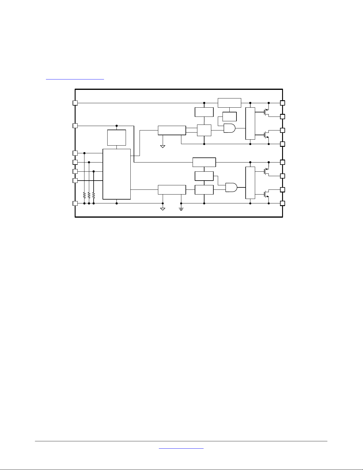
on die junction temperature of the device. As shown in Figure 2, the
Schmitt trigger, EN, HIN and LIN inputs are internally pulled LOW to
assure the driver is always in a default ‘OFF’ state during initial
application of V
by the DT pin and can be configured to prevent or allow
cross−conduction.
bias. Programmable dead−time control is available
DD
DD
bias
EVAL BOARD USER’S MANUAL
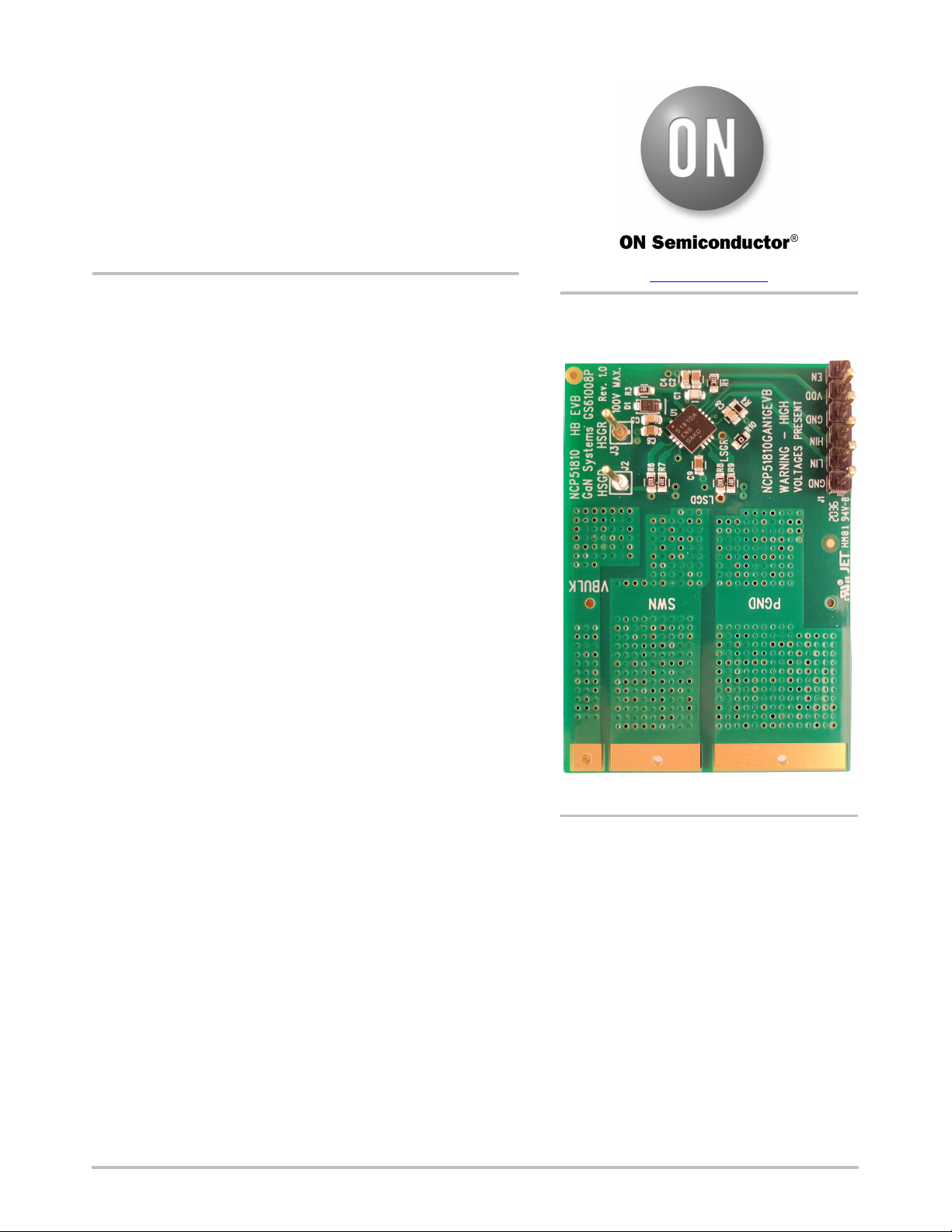
Figure 1. Evaluation Board Photo
© Semiconductor Components Industries, LLC, 2020
October, 2020 − Rev. 0
1 Publication Order Number:
EVBUM2762/D
Page 2
NCP51810GAN1GEVB
The NCP51810 can be considered as having two
independent high−side and low−side “floating” drive stages.
The high−side can float up to 100 V referenced to SW and
the low−side can float up to 3.5 V referenced to PGND,
making it well suited for applications where the driver has
to float above a low−side current sense resistor as described
in “Connection Method #2
VBST
VDD
EN
HIN
LIN
DT
SGND
” section. Each drive stage
VDD
UVLO
8.5V/8V
(ON/OFF)
SCHMITT
TRIGGER INPUT
SHOOT THOUGH
PREVENTION
CYCLE−By−
CYCLE EDGE
TRIGGERED
SHUTDOWN
DEAD−TIME
MODE CONTROL
LEVEL SHIFTER
LEVEL SHIFTER
includes dedicated input level shifting to ensure accurately
matched propagation delays to within 5 ns. Each output
includes separate source and sink allowing rise and fall times
to be set independently with a single resistor, eliminating
additional, discrete circuitry often required for high−speed
turn−off.
VDDH
VBST
UVLO
HO
LO
S
R
VDDL
REGULATOR
VDDL
UVLO
DELAY
REGULATOR
VDDH
UVLO
R
Q
DRIVER
DRIVER
VDDH
HOSRC
HOSNK
SW
VDDL
LOSRC
LOSNK
PGND
Figure 2. NCP51810, Functional Block Diagram
NCP51810 HB GaN Driver EVB Description
The NCP51810 HB GaN Driver EVB is designed using an
1880 mil x 1310 mil, four−layer printed circuit board (PCB)
and includes the NCP51810 GaN driver, two E−mode GaN
power switches connected in a high−side, low−side
configuration and all necessary drive circuitry. The EVB
does not include a PWM controller, and is generic from the
point of view that it is not dedicated to any one topology, and
can be used in any topology that requires the use of
a high−side/low−side FET combination. The EVB can be
connected into an existing power supply, and will replace the
HS/LS driver and MOSFETs. The EVB has preset, but
configurable dead−time control and driver enable/disable.
The GaN power switches are rated up to 100 V, 90 A, making
them well suited for half−bridge topologies operating from
an output in the range of 100 V. However, due to R
DS(ON)
temperature dependence, the maximum, practical case
temperature should not exceed ~90°C (90°C = 1.6 x
R
, normalized at 25°C). The EVB has only 27
DS(ON)
components and its small size allows it to be installed in tight
areas. Even with the small size, several pins are available to
probe the circuit. HS and LS gate drives, as well as SWN are
accessible. Note: In half−bridge operation, the HS gate drive
can only be probed with a high−voltage differential probe on
the Hi−Side Gate Drive (HSGD) pin and the Hi−Side Gate
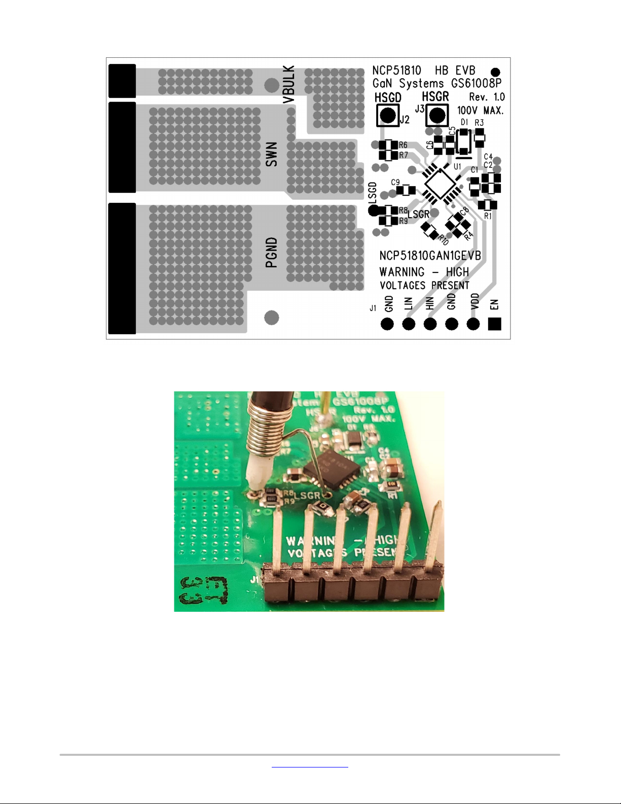
Return (HSGR) pin. The LS gate drive has two plated holes
for a tip−and−barrel probe measurement (LSGD). The
plated hole closest to the NCP51810 is probe GND, as
shown in Figure 3. A tip−and−barrel measurement is
performed by removing the “hat” from a passive probe and
using the probe “pin” for the measurement and a spring pin
fit on the GND barrel of the probe for ground. Figure 4
shows the typical tip−and−barrel measurement method for
LSGD using a LeCroy passive probe and GND spring.
www.onsemi.com
2
Page 3
NCP51810GAN1GEVB
Figure 3. NCP51810 HB GaN Driver EVB
Figure 4. Tip−and−Barrel Measurement Method
www.onsemi.com
3
Page 4
NCP51810 EVB Schematic
NCP51810GAN1GEVB
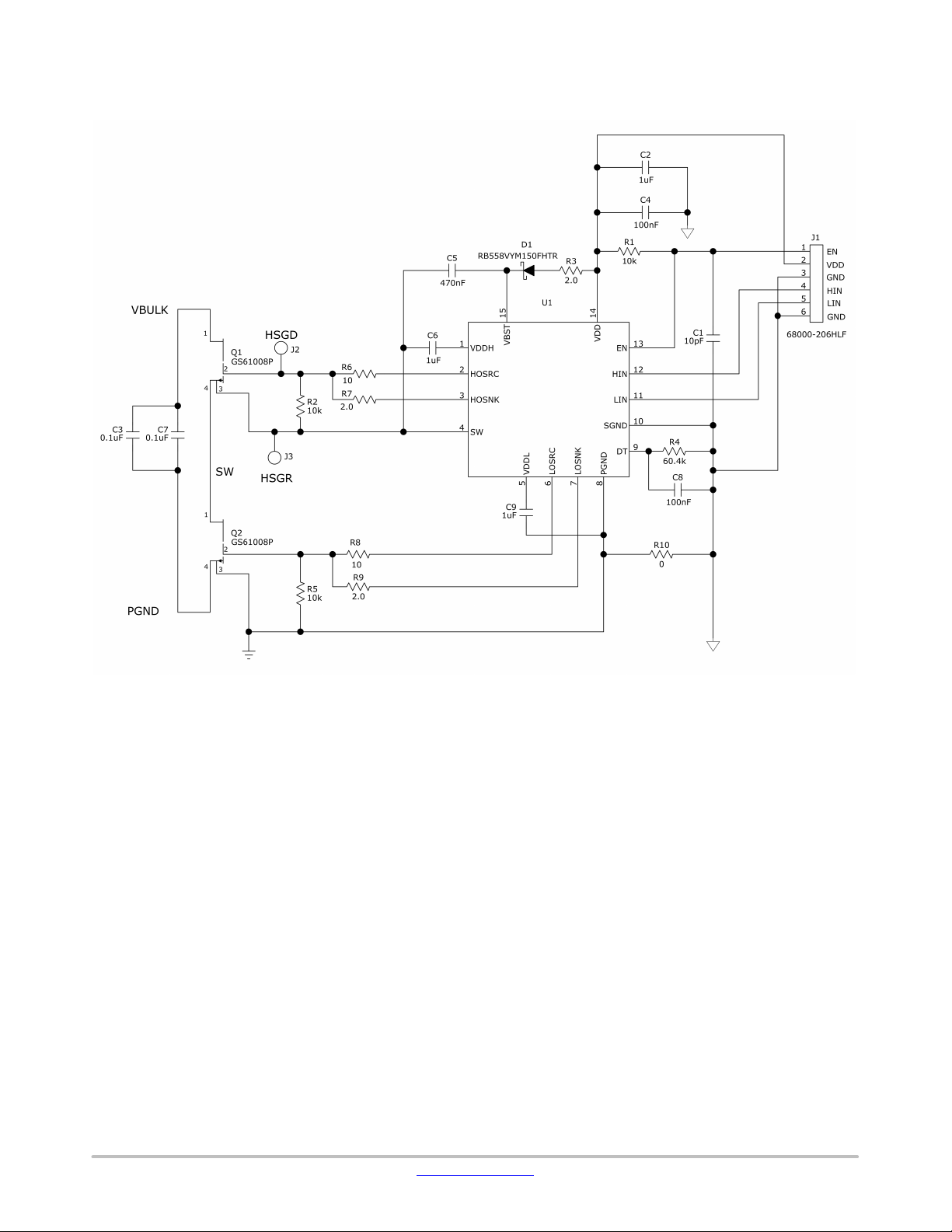
Figure 5. NCP51810 EVB Schematic
www.onsemi.com
4
Page 5

NCP51810GAN1GEVB
NCP51810 EVB Bill of Materials (BOM)
Table 1. NCP51810 EVB BILL OF MATERIALS
Item Qty Reference Value Part Number Description Manufacturer Pkg Type
1 1 C1 10 pF CC0603JRNPO9BN100 CAP, SMD, CERAMIC, 50 V, NPO Yageo 603
2 1 C5 470 nF CC0603KRX7R8BB474 CAP, SMD, CERAMIC, 25 V, X7R Yageo 603
3 3 C2 C6 C9
4 2 C3 C7
5 2 C4 C8 100 nF CC0603KRX7R8BB104 CAP, SMD, CERAMIC, 25 V, X7R Yageo 603
6 1 D1 RB558VYM150FHTR Diode_Shottky, 150 V,
7 1 J1 68000−206HLF Header, SIP6 100mil pitch,
8 2 J2−3 1352−1 Testpin, Gold, 40 mil, 28 mil solder
9 2 Q1−2 GS61008P GaNFET, 100 V, E−mode,
10 1 R4 (Note 1)
11 1 R10 (Note 2)
12 3 R1−2 R5
13 3 R3 R7 R9
14 2 R6 R8
15 1 U1 NCP51810 High Speed Half Bridge GaN Driver,
1 mF
0.1 mF
60.4 kW
0 W
10 kW
2 W
10 W
1. R4 used to set dead−time (DT).
2. R10 used to connect SGND to LS gate return.
CL10B105KA8NNNC CAP, SMD, CERAMIC, 25 V, X7R Samsung 603
C1206J104K2RAC7800 CAP, SMD, CERAMIC, 200 V, X7R Kemet 1206
500 mA, 6.35 ns RR
Post − 95 mil, Mate − 230 mil
length
90 A, 7 mW, Kelvin Source
RMCF0603FT60K4 RES, SMD, 1/10 W Stackpole 603
RC0603JR−070RL RES, SMD, 1/10 W Yageo 603
RC0603FR−0710KL RES, SMD, 1/10 W Yageo 603
CPF0603F2R0C1 RES, SMD, 1/10 W TE Connectivity 603
RC0603FR−0710RL RES, SMD, 1/10 W Yageo 603
200 V
Rohm SOD−323
Amphenol Thru−Hole
Keystone Thru−Hole
GaN Systems 7.55 x 4.59 mm
ON Semiconductor MLP 4x4−15
www.onsemi.com
5
Page 6

NCP51810GAN1GEVB
NCP51810 Layers
• Top Layer: The large copper high current carrying etches
used to connect the HS/LS GaN power switches also act
as heat spreaders. A heatsink (if utilized) will be attached
to this layer.
• Layer 2 (Internal): This layer has a shielding plane for
the driver and driver components as well as additional
high current carrying etches for the HS/LS GaN power
switches.
• Layer 3 (Internal): Layer 3 has additional high current
carrying etches for the HS/LS GaN power switches.
• Bottom Layer: The high current carrying etches for the
HS/LS GaN power switches on the bottom layer also act
as heat spreaders.
Top Layer Layer 2, Internal
Layer 3, Internal Bottom Layer
Figure 6. PCB Assembly and Layers
www.onsemi.com
6
Page 7
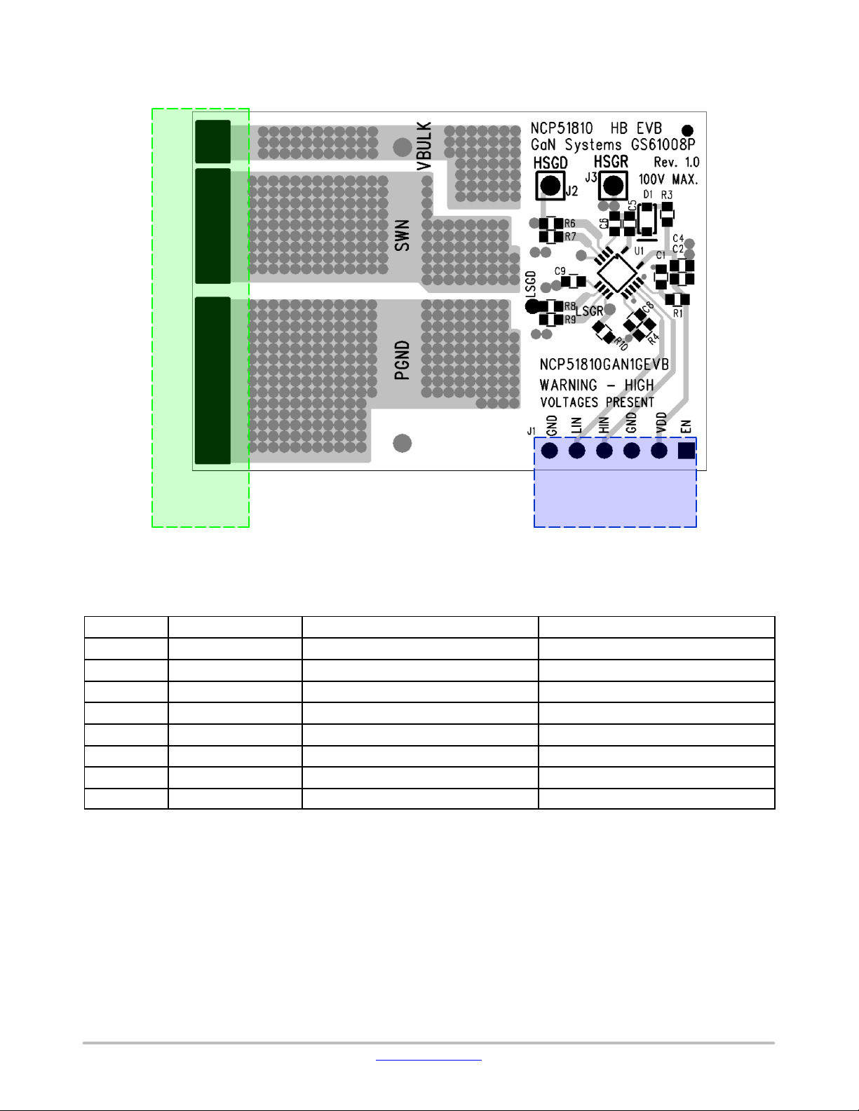
NCP51810 EVB I/C Connections
NCP51810GAN1GEVB
654321
Power Stage
Input Connector
Figure 7. EVB I/O Connections
Table 2. I/O CONNECTOR DESCRIPTION
Pin Name Pin Type Description Value
EN (Note 3) J1−1 Logic input for enabling/disabling the driver 2.5 V < EN < VDD + 0.3 V
VDD J1−2 Bias voltage for high current driver 8 V < V
GND J1−3,6 Signal ground on the driver 0 V
HIN J1−4 Logic input for high−side gate driver 0 V < HIN < VDD + 0.3 V
LIN J1−5 Logic input for low−side gate driver 0 V < LIN < VDD + 0.3 V
VBULK PAD VIN connection 100 V max
SWN PAD Switch Node connection 100 V max
PGND PAD Power Ground connection 0 V
3. EN pin tied to driver VDD through 10 kW resistor (R1) on EVB.
DD
< 20 V
www.onsemi.com
7
Page 8

NCP51810GAN1GEVB
NCP51810 EVB CONNECTION METHODS
There are two different methods for connecting the EVB
to an existing power board.
Power topologies not using a current sense resistor
connected in series with the LS GaN power switch source
(a current sense transformer or other method of sensing
current used) will use Connection Method #1, shown in
“Connection Method #1
Power topologies using a current sense resistor (R
connected in series with the LS GaN source, will use
Connection Method #2, shown in “Connection Method #2
section.
” section.
CS
Preparing Power Board for EVB Connection
1. Remove HS and LS MOSFETs and HS and LS gate
drive resistors from the power board as illustrated in
Figure 8.
2. Remove any gate turn off circuitry. This is any
circuit used to help drive the gate to 0 V during turn
off.
)
3. Before connecting the EVB, ensure that VDD, HIN,
LIN, and VBULK are within the parameters listed in
”
Table 2.
Figure 8. Power Board Preparation
Connection Method #1 − No GaN LS Current Sense
Resistor on Power Board
Connect the EVB as shown in Figure 9. AWG #22 wire is
suggested for LIN, HIN and VDD. AWG #18 or larger wire
is suggested for VBULK, SWN and PGND. Keeping both
the Input connections and the VBLK, SWN and PGND
connections as short as possible is preferred.
Connection Method #2 − LS GaN Current Sense
Resistor (R
) Present on Power Board
CS
Low−power applications, such as an active−clamp
flyback or forward converter often use a current sensing
resistor, R
, located in the low−side GaN power
CS
switch-source leg. In such applications, the EVB PGND and
SGND pins must be isolated on the EVB (normally connected
by R10) because R
would essentially be shorted through
CS
this resistor if not removed. The NCP51810 low−side drive
circuit is able to withstand −3.5 V to +3.5 V of common mode
voltage. Since most current sense voltage signals are less than
1 V, the low−side drive stage can easily “float” above the
voltage, V
, generated by the current sense resistor.
RCS
Connection Method #2: Remove R10 on the EVB to
isolate LS gate drive return from GND as shown in
Figure 10 and Figure 13. Failure to remove R10 will short
out R
. Connect the EVB as shown in Figure 10. AWG #22
CS
wire is suggested for LIN, HIN and VDD. AWG #18 or
larger wire is suggested for VBULK, SWN and PGND.
Keeping both the input and power connections as short as
possible is preferred.
www.onsemi.com
8
Page 9

NCP51810GAN1GEVB
+
PWM
CONTROLLER
PAIR
TWISTED
PAIR
R10
+
VBULK
LS
HS
SWN
PGND
LOUT
HOUT
TWISTED
INSTALLED
Figure 9. Connection Method #1 − No LS Current Sense Resistor
VDD
GND
FLOATING
AT VCS
CS
RESISTOR
+
PWM
CONTROLLER
CS
PAIR
TWISTED
PAIR
R10
VDD
VDD
GND
GND
+
VBULK
LS
SWN
HS
PGND
VCS
LOUT
HOUT
TWISTED
REMOVED
Figure 10. Connection Method #2 − LS Current Sense Resistor on Power Board
www.onsemi.com
9
Page 10

NCP51810GAN1GEVB
External VDD
An external VDD can be used, as long as the HIN and LIN
signals still fall within the parameters listed in Table 2. If an
external VDD is used, the external VDD GND connection
must be connected to the power board VDD GND, as shown
in Figure 11. An external VDD can be used for boards either
with or without an LS Current Sense Resistor. When using
an external VDD, put a 1N4148 blocking diode (or similar
+
60 V, 1A minimum diode) in series with VDD + to protect
the VDD supply. It’s also suggested to put a small
electrolytic decoupling capacitor (example: 22 mF, 35 V)
across the External VDD supply output, as shown in
Figure 11. VDD voltage should be measured and set after
the blocking diode to take into account the voltage drop
across the diode.
PGND
LS
+
VBULK
Figure 11. External VDD Connection
SWN
HS
CONTROLLER
LOUT
HOUT
TWISTED
PAIR
TWISTED
PAIR
R10
INSTALLED
PWM
VDD
GND
+
Decoupling
(8 V < VDD < 20 V)
−
+
Capacitor
External VDD
Thermal Considerations
Applications where higher currents could cause GaN
power switch temperatures to exceed 90°C (such as a high
power, synchronous buck), a voltage−isolated adhesive
heatsink can be attached to the top of the EVB. The GaN
power switches on this EVB are bottom−cooled. Copper
heat spreaders are part of the top and bottom layer of this
EVB. A voltage−isolated adhesive heatsink attached to the
EVB top will aid in reducing the GaN power switch
temperatures. Figure 12 shows the positioning of a heatsink.
www.onsemi.com
Figure 12. NCP51810 HB GaN Driver EVB
and Heatsink
10
Page 11

CONFIGURING ENABLE (EN)
AND DEAD−TIME (DT)
NCP51810GAN1GEVB
EN Function and External Control
The NCP51810 GaN Driver EN is internally pulled low
to SGND, so the driver is always defaulted to a disabled
output status. Similar to HIN and LIN, EN is a Schmitt
trigger TTL compatible input. Pulling the EN pin above
2.5 V typical, enables the outputs, placing the NCP51810
into an active ready state. Due to the nature of high−speed
switching associated with GaN power stages, and for
improved noise immunity, the EN pin is tied to V
through
DD
a 10−kW (R1) pull−up resistor and is bypassed by a 10 pF
capacitor (C1). If an external enable signal is preferred, the
external enable signal must conform to the value limits listed
in Table 2. More information on EN control can be found in
the NCP51810 datasheet
.
When using an external active enable signal, remove R1
and connect a signal to the EN pin on the EVB. The external
enable signal GND must connect to the EVB GND. The
10 pF EN bypass capacitor (C1) on the EVB must remain
installed. Refer to Figure 13 for R1 and C1 locations.
DT Function and Mode Configuration
Accurately ensuring some minimal amount of dead−time
between the high−side and low−side gate drive output
signals is critical for safe, reliable optimized operation of
any high−speed, half−bridge power stage. The NCP51810
uses a voltage−configured, dead−time control pin (DT). The
NCP51810 offers four unique mode settings to utilize
dead−time in such a way to be fully compatible with any
control algorithm.
The EVB dead−time is preset to Mode B by a single,
60.4 kW resistor (R4) connected between the DT and SGND
pins. This sets the dead−time voltage to 1.3 V, proportional
to approximately 65 ns of dead−time. When adjusting the
dead−time is required, the resistor value can be changed,
which will change the voltage level on the DT pin. Follow
the instructions outlined In DT Mode Descriptions to change
DT modes. For noise immunity, the DT pin is bypassed with
a 0.1 mF capacitor (C8). This capacitor must not be removed.
More information on dead−time control can be found in the
NCP51810 datasheet
. Refer to Figure 13 for R4 and C8
locations.
DT Mode Descriptions
1. MODE A:
voltage, V
Connect DT to SGND; When the DT pin
, is less than 0.5 V typical (RDT=0W),
DT
the DT programmability is disabled and fixed
dead−time, anti−cross−conduction protection is
enabled. If HIN and LIN are overlapping by X ns,
then X ns of dead−time is automatically inserted.
Conversely, if HIN and LIN have greater than 0 ns
of dead−time then the dead−time is not modified by
the NCP51810 and is passed through to the output
stage as defined by the controller. This type of
dead−time control is preferred when the controller
will be making the necessary dead−time adjustments
but needs to rely on the NCP51810 dead−time
control function for anti−cross−conduction
protection.
2. MODE B:
Connect a 25 kW <RDT< 200 kW
Resistor from DT to SGND; Dead−time is
programmable by a single resistor connected
between the DT and SGND pins. The amount of
desired dead time can be programmed via the dead
time resistor, R
< 200 kW to obtain an equivalent dead−time,
R
DT
proportional to R
, between the range of 25 kW <
DT
, in the range of 25 ns < t
DT
200 ns. If either edge between HIN and LIN result in
a dead−time less than the amount set by R
, the set
DT
DT value shall be dominant. If either edge between
HIN and LIN result in a dead−time greater than the
amount set by R
, the controller dead−time shall be
DT
dominant.
3. MODE C:
Connect a 249 kW Resistor from DT to
SGND; Connect a 249 kW resistor between DT and
SGND to program the maximum dead−time value of
200 ns. The control voltage range, V
t
= 200 ns is 4 V < V
DT
4. MODE D:
voltage, V
Connect DT to VDD; When the DT pin
, is greater than 6 V (pulled up to VDD
DT
DT
< 5 V.
, for assuring
DT
through 10 kW resistor), anti−cross−conduction
protection is disabled, allowing the output signals to
overlap. If choosing this operating mode while
driving a half−bridge power stage, extreme caution
should be taken, as cross conduction can potentially
damage power components if not accounted for.
This type of dead−time control is preferred when the
controller will be making extremely accurate
dead−time adjustments and can respond to the
potential of over−current faults on a cycle−by−cycle
basis.
DT
<
www.onsemi.com
11
Page 12

NCP51810GAN1GEVB
EN Bypass
Capacitor
EN Resistor
DT Bypass
Capacitor
DT Resistor
SGND = PGND
Resistor
Figure 13. EN and DT Resistor and Capacitor Locations
CONCLUSION
When using this EVB with an existing silicon (Si)
half−bridge power stage at normal Si frequencies
(40−500 kHz), the true benefits of GaN technology (higher
running frequencies, smaller magnetics, higher power
density) will not be realized at the lower frequencies that Si
typically operates. The goal of this EVB is to easily enable
the evaluation of the NCP51810 GaN driver, mating it with
existing half−bridge power topologies, and not to
significantly change their operation or efficiency. This EVB
can be run at high frequencies, but care must be applied to
both the input signals and the power connections to be as
short as possible to avoid noise injection and ringing. More
information on GaN driver PCB design and layout
techniques are available at ON Semiconductor/NCP51810
.
www.onsemi.com
12
Page 13

ON Semiconductor and the ON Semiconductor logo are trademarks of Semiconductor Components Industries, LLC dba ON Semiconductor or its subsidiaries in the United States and/or
other countries. ON Semiconductor owns the rights to a number of patents, trademarks, copyrights, trade secrets, and other intellectual property. A listing of ON Semiconductor’s
product/patent coverage may be accessed at www.onsemi.com/site/pdf/Patent−Marking.pdf
subject to all applicable copyright laws and is not for resale in any manner.
The evaluation board/kit (research and development board/kit) (hereinafter the “board”) is not a finished product and is as such not available for sale to consumers. The board is only intended
for research, development, demonstration and evaluation purposes and should as such only be used in laboratory/development areas by persons with an engineering/technical training
and familiar with the risks associated with handling electrical/mechanical components, systems and subsystems. This person assumes full responsibility/liability for proper and safe handling.
Any other use, resale or redistribution for any other purpose is strictly prohibited.
The board is delivered “AS IS” and without warranty of any kind including, but not limited to, that the board is production−worthy, that the functions contained in the board will meet your
requirements, or that the operation of the board will be uninterrupted or error free. ON Semiconductor expressly disclaims all warranties, express, implied or otherwise, including without
limitation, warranties of fitness for a particular purpose and non−infringement of intellectual property rights.
ON Semiconductor reserves the right to make changes without further notice to any board.
You are responsible for determining whether the board will be suitable for your intended use or application or will achieve your intended results. Prior to using or distributing any systems
that have been evaluated, designed or tested using the board, you agree to test and validate your design to confirm the functionality for your application. Any technical, applications or design
information or advice, quality characterization, reliability data or other services provided by ON Semiconductor shall not constitute any representation or warranty by ON Semiconductor,
and no additional obligations or liabilities shall arise from ON Semiconductor having provided such information or services.
The boards are not designed, intended, or authorized for use in life support systems, or any FDA Class 3 medical devices or medical devices with a similar or equivalent classification in
a foreign jurisdiction, or any devices intended for implantation in the human body. Should you purchase or use the board for any such unintended or unauthorized application, you shall
indemnify and hold ON Semiconductor and its officers, employees, subsidiaries, affiliates, and distributors harmless against all claims, costs, damages, and expenses, and reasonable
attorney fees arising out of, directly or indirectly, any claim of personal injury or death associated with such unintended or unauthorized use, even if such claim alleges that ON Semiconductor
was negligent regarding the design or manufacture of the board.
This evaluation board/kit does not fall within the scope of the European Union directives regarding electromagnetic compatibility, restricted substances (RoHS), recycling (WEEE), FCC,
CE or UL, and may not meet the technical requirements of these or other related directives.
FCC WARNING – This evaluation board/kit is intended for use for engineering development, demonstration, or evaluation purposes only and is not considered by ON Semiconductor to
be a finished end product fit for general consumer use. It may generate, use, or radiate radio frequency energy and has not been tested for compliance with the limits of computing devices
pursuant to part 15 of FCC rules, which are designed to provide reasonable protection against radio frequency interference. Operation of this equipment may cause interference with radio
communications, in which case the user shall be responsible, at its expense, to take whatever measures may be required to correct this interference.
ON Semiconductor does not convey any license under its patent rights nor the rights of others.
LIMITATIONS OF LIABILITY: ON Semiconductor shall not be liable for any special, consequential, incidental, indirect or punitive damages, including, but not limited to the costs of
requalification, delay, loss of profits or goodwill, arising out of or in connection with the board, even if ON Semiconductor is advised of the possibility of such damages. In no event shall
ON Semiconductor’s aggregate liability from any obligation arising out of or in connection with the board, under any theory of liability, exceed the purchase price paid for the board, if any.
For more information and documentation, please visit www.onsemi.com
.
. ON Semiconductor is an Equal Opportunity/Affirmative Action Employer. This literature is
PUBLICATION ORDERING INFORMATION
LITERATURE FULFILLMENT:
Email Requests to: orderlit@onsemi.com
ON Semiconductor Website: www.onsemi.com
TECHNICAL SUPPORT
North American Technical Support:
Voice Mail: 1 800−282−9855 Toll Free USA/Canada
Phone: 011 421 33 790 2910
Europe, Middle East and Africa Technical Support:
Phone: 00421 33 790 2910
For additional information, please contact your local Sales Representative
◊
www.onsemi.com
1
 Loading...