

Page 1

EVBUM2528/D
NCP51705 Mini Evaluation
Board User'sManual
NCP51705 SiC Driver Evaluation Board
for Existing or New PCB Designs
www.onsemi.com
INTRODUCTION
Purpose
This document describes the use and applications for the
NCP51705 SiC driver mini EVB. The EVB is designed on
a four layer PCB and includes the NCP51705 driver and all
the necessary drive circuitry. The EVB also includes an
on−board digital isolator and the ability to solder any
MOSFET or SiC MOSFET in a T0247 high voltage
package. The EVB does not include a power stage and is
generic from the point of view that it is not dedicated to any
particular topology. It can be used in any low−side or
high−side power switching application. For bridge
configurations two or more of these EVBs can be configured
in a totem pole type drive configuration. The EVB can be
considered as an isolator+driver+T0247 discrete module.
NCP51705 Description
The NCP51705 driver is designed to primarily drive SiC
MOSFET transistors. To achieve the lowest possible
EVAL BOARD USER’S MANUAL
conduction losses, the driver is capable of delivering the
maximum allowable gate voltage to the SiC MOSFET
device. By providing high peak current during turn−on and
turn−off, switching losses are also minimized. For improved
reliability, dV/dt immunity and even faster turn−off, the
NCP51705 can utilize its on−board charge pump to generate
a user selectable negative voltage rail.
For full compatibility and to minimize the complexity of
the bias solution in isolated gate drive applications the
NCP51705 also provides an externally accessible 5V rail to
power the secondary side of digital or high speed opto
isolators.
The NCP51705 offers important protection functions
such as under−voltage lockout monitoring for the bias power
and thermal shutdown based on the junction temperature of
the driver circuit.
© Semiconductor Components Industries, LLC, 2017
December, 2017 − Rev. 0
1 Publication Order Number:
EVBUM2528/D
Page 2
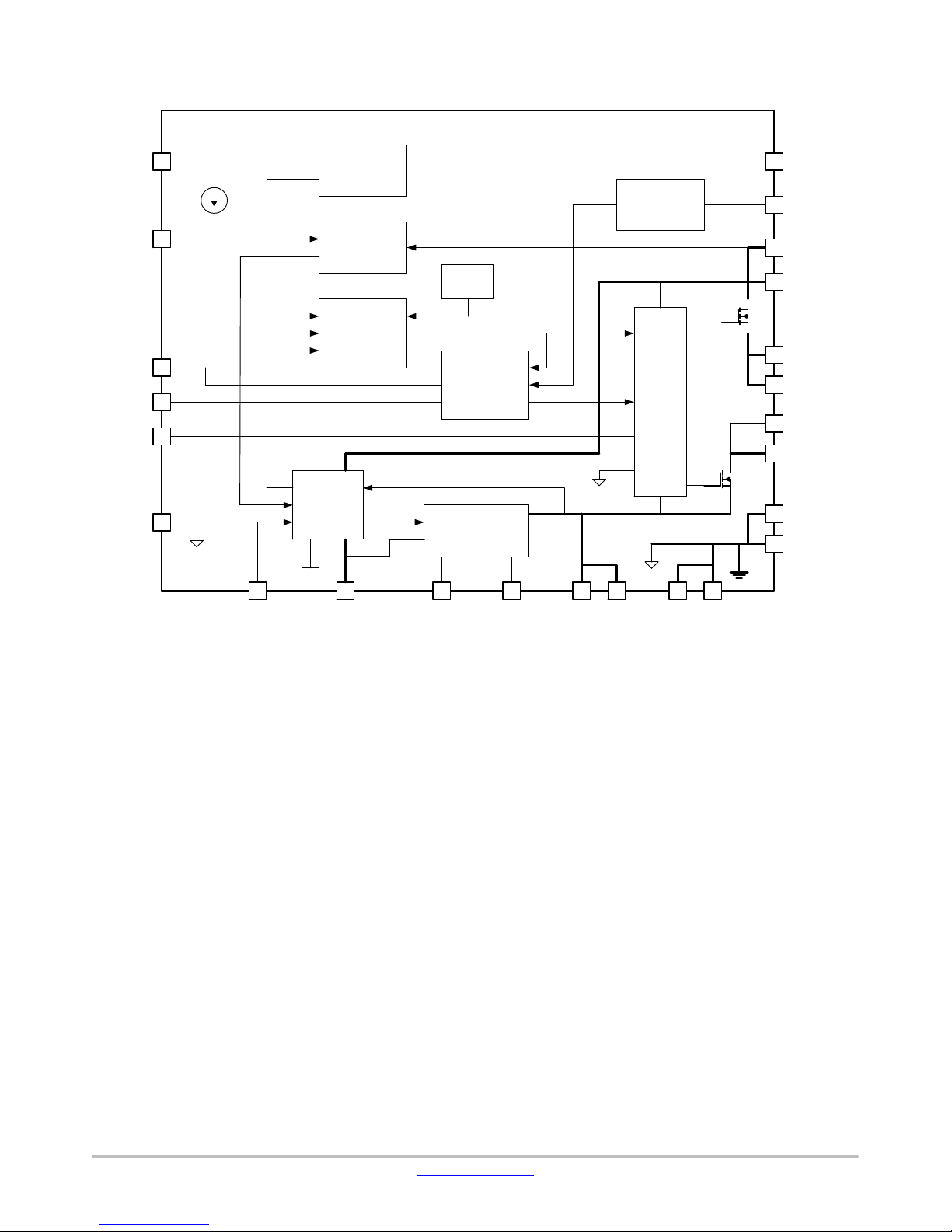
NCP51705 Block Diagram
EVBUM2528/D
NCP51705
V5V
UVSET
IN+
IN-
XEN
SGND
23
25
mA
5V REG
DESAT /
CURRENT
SENSE
24
UVLO
TSD
21
22
20
19
SVDD
DESAT
/CS
VDD
VDD
5V_OK
VDD_OK
VEE_OK
1
PROTECTION
LOGIC
INPUT LOGIC
2
3
RUN
DRIVER
LOGIC
&
LEVEL
SHIFT
18
17
14
13
OUTSRC
OUTSRC
OUTSNK
OUTSNK
CHARGE
4
PUMP REG
CPCLK
CHARGE PUMP
POWER STAGE
5
VEESET
6
VCH
7
C+
8
C-
11 12 9 10
VEE
VEE
PGND
PGND
PGND
16
PGND
15
Figure 1. NCP51705 Functional Block Diagram
www.onsemi.com
2
Page 3
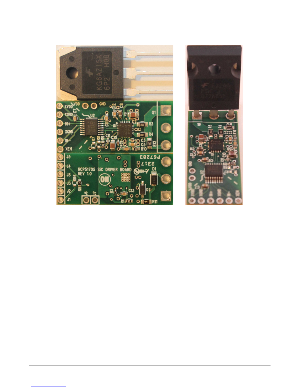
SUMMARY OF EVB
EVB Photos
EVBUM2528/D
Figure 2. NCP51705 EVB (35 mm x 15 mm x 5 mm) − Top and Bottom View (T0−247 Shown for Scale)
www.onsemi.com
3
Page 4
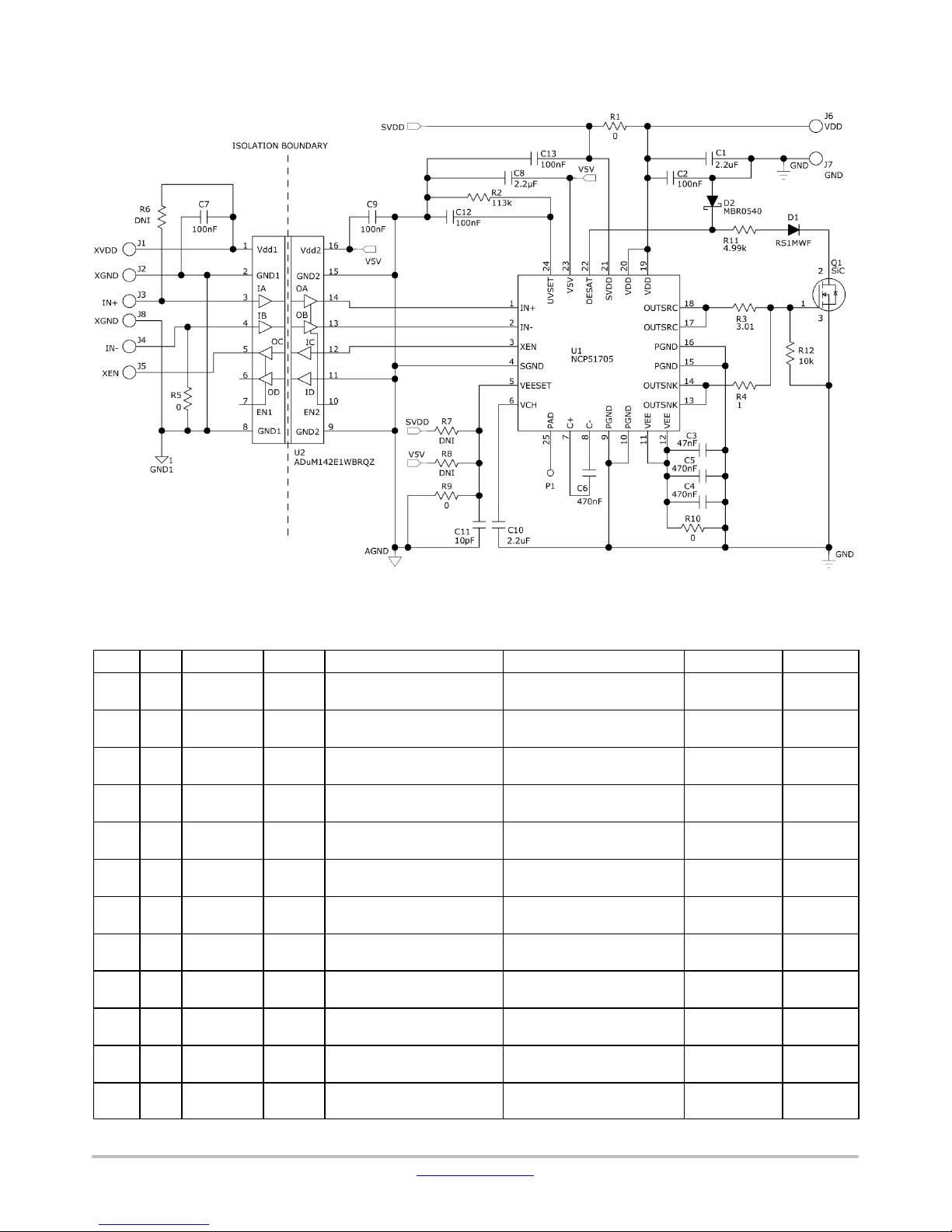
EVB Schematic
EVBUM2528/D
Figure 3. NCP51705 EVB Schematic
Table 1. BILL OF MATERIALS
Item Qty Reference Value Part Number Description Manufacturer Pkg Type
1 2 C1 C10
2 2 C2 C13 100 nF C1005X7R1H104M050BE CAP, SMD, CERAMIC, 50 V,
3 1 C3 47 nF GRM155R71E473KA88D CAP, SMD, CERAMIC, 25 V,
4 2 C4−5 470 nF GRM188R71E474KA12D CAP, SMD, CERAMIC, 25 V,
5 1 C6 470 nF C1005X5R1E474K050BB CAP, SMD, CERAMIC, 25 V,
6 3 C7 C9
C12
7 1 C8
8 1 C11 10 pF GRM1555C1H100JA01D CAP, SMD, CERAMIC, 50 V,
9 1 D1 RS1MWF Diode, Fast, 1 A, 1000 V,
10 1 D2 MBR0540 Diode, Shottky, 40 V,
11 1 Q1 DNI MOSFET, N−CH, 600 V,
12 4 R1 R5
R9−10
2.2 mF
100 nF C0603C104K8RACTU CAP, SMD, CERAMIC, 10 V,
2.2 mF
CGA4J3X7R1H225M125AE CAP, SMD, CERAMIC, 50 V,
X7R
X7R
X7R
X7R
X5R
X7R
LMK107B7225KA−T CAP, SMD, CERAMIC, 10 V,
X7R
NPO
Std. Rec.
500 mA, 510 mV
20 A, 190 mW
0 RC0603JR−070RL RES, SMD, 1/10 W STD 603
STD 805
STD 402
STD 402
STD 603
STD 402
STD 603
STD 603
STD 402
Vishay SOD123F
ON
Semiconductor
ON
Semiconductor
SOD−123
TO−247
www.onsemi.com
4
Page 5
EVBUM2528/D
Table 1. BILL OF MATERIALS
Item Pkg TypeManufacturerDescriptionPart NumberValueReferenceQty
13 1 R2 113k RC0402FR−07200KL RES, SMD, 1/16 W STD 402
14 1 R3 3.01 RMCF0805FT3R01
15 1 R4 1 RMCF0805FT1R00
16 3 R6−8 DNI RES, SMD, 1/10 W STD 603
17 1 R11 4.99k RC0805FR−074K99L
18 1 R12 10k RC0805FR−0710KL RES, SMD, 1/8 W STD 805
19 1 U1 NCP51705 SiC Driver, Single, 6 A,
20 1 U2 ADuM142E1WBRQZ Digital Isolator, RF, 4−Chan-
RES, SMD, 1/8 W
RES, SMD, 1/8 W
RES, SMD, 1/8 W
Single
nel
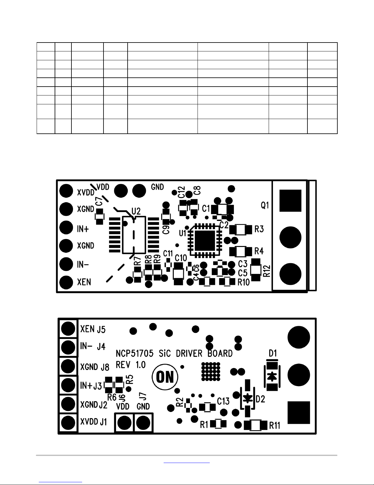
PCB Assembly and Layers
Figure 4 through Figure 9 shows the top and bottom
assembly and the four−layers of the PCB. The PCB is 35 mm
x 15 mm x 5 mm (length x width x height) where the width
of the PCB is approximately the width of a T0−247 body.
STD 805
STD 805
STD 805
ON
Semiconductor
Analog
Devices
WQFN−24
QSOP−16
Figure 4. Top Assembly
Figure 5. Bottom Assembly
www.onsemi.com
5
Page 6

EVBUM2528/D
Figure 6. Top Layer
Figure 7. Layer 2
Figure 8. Layer 3
www.onsemi.com
6
Page 7

EVBUM2528/D
Figure 9. Bottom Layer
I/O Connectors
There are 7 I/O connectors described in Table 2 below.
The mC (or, PWM control IC) output (J3, J4), the XVDD and
XGND (J1, J2) and the XEN (J5) signals are noted as
“primary” ground referenced. There is no true “primary”
and “secondary” ground but there is 1.5 kV galvanic
isolation across the isolation boundary. It is especially
important to maintain isolation in high−side, high−voltage,
switching applications where the “secondary” VDD (J6, J7)
floats VDD volts above the power supply input voltage:
Table 2. I/O CONNECTOR DESCRIPTIONS
Ref Des Name I/O GND Ref Type Description Value (V)
J1 XGND Input Primary Plated Hole External primary ground from PWM side 0
J2 XVDD Input Primary Plated Hole External VDD from PWM side (isolator bias) 5
(Note 1)
J3 IN+ Input Primary Plated Hole Non−inverting, PWM input 3.3<V
J4 IN− Input Primary Plated Hole Inverting PWM input
J5 XEN Output Primary Plated Hole XEN fault flag or sync signal from NCP51705 5
J6 VDD Input Secondary Plated Hole NCP51705 VDD <20
J7 GND Input Secondary Plated Hole NCP51705 secondary ground 0
J8 XGND Input Primary Plated Hole External primary ground from PWM side 0
1. The digital isolator, U2, requires that the amplitude of the PWM input (IN+ or IN−) be equal to VDD (XVDD) and less than or equal to 5 V.
3.3<V
IN+
(Note 1)
IN
(Note 1)
<5
<5
-
www.onsemi.com
7
Page 8

EVBUM2528/D
EVB INSTALL CONFIGURATIONS
Mounting into Existing PCB − Option 1
The NCP51705, SiC Driver Mini EVB can be mounted
into an existing power board, shown as “Main PCB” in
Figure 10. If there are no components or low profile surface
mount components only, the mini EVB can be mounted
parallel to the main PCB as shown in Figure 10. The T0−247,
SiC MOSFET leads would pass through the mini EVB
plated thru−holes and into the main PCB. Or, if necessary,
the gate lead of the T0−247, SiC MOSFET can be soldered
to the plated thru−hole on the mini EVB and cut so that it
does not contact the main PCB, as shown in the dotted box
in Figure 10. For mechanical strength, it is preferred that the
T0−247 gate lead pass through both PCB’s.
T0−247
SiC
PWM Input
(flying lead)
Kapton tape
Mini EVB
Main PCB
S
Side View
Figure 10. Mini EVB Installation − Option 1
Recommended Procedure for Option 1 Mounting into an
Existing PCB
1. On the main PCB, isolate the gate drive to the
T0−247 SiC MOSFET. If the existing design
includes a gate drive resistor, removing it should
serve the purpose of isolating the gate drive to the
T0−247. If there is no series component between
the PWM signal source and the T0−247 gate lead,
the gate drive PCB track will need to be cut.
2. Measure the resistance between the PWM source
and the T0−247 gate lead (or PWM source to gate
drive transformer/isolator if applicable). Verify
reading is high impedance (open).
3. If a T0−247 discrete is installed in the main PCB,
remove it now.
4. Place Kapton or non−conductive tape over the
main PCB area directly beneath the mini EVB.
This is to avoid the possibility of having any
components on the bottom of the mini EVB touch
components or conductive surfaces on the main
PCB.
5. Solder a flying lead of bus wire to the main PCB,
PWM signal. Make sure there is enough length of
the PWM input (flying lead) to reach through the
mini EVB plated thru−hole (J3 or J4)
6. For non−inverting PWM input logic, verify that
R5 (0 W) is installed and R6 is removed. This is
the correct configuration of the mini EVB for
non−inverting PWM input logic.
Option – Cut T0−247 gate lead
T0−247
SiC
Mini EVB
Kapton tape
GDS
Back View
T0−247
SiC
Mini EVB
Main PCB
GDS
7. For inverting PWM input logic, verify that R6
(0 W) is installed and R5 is removed. This is the
correct configuration of the mini EVB for
inverting PWM input logic.
8. Solder the T0−247 through just the mini EVB first
9. With the T0−247 installed into the mini EVB,
install and solder the T0−247 leads into the main
PCB
10. Solder the other end of the PWM input (flying
lead) to IN+ (J3) for non−inverting PWM
applications or IN− (J4) for inverting PWM
applications.
11. Using the same size bus wire, solder the remaining
connections between J1, J2, J5 and J8 of the mini
EVB to the appropriate locations on the main
PCB.
12. Solder flying leads from J6−7 for bias voltage to
the NCP51705. Note that J6−7 are across the
isolation boundary from J1−5 and J8.
Mounting into Existing PCB − Option 2
If components mounted on the main PCB interfere with
mounting the mini EVB as described by Option 1
(Figure 10), the T0−247 leads can be formed (lead length
may need to be added) with the mini EVB mounted
perpendicular to the main PCB as shown in Figure 11, option
2. If required, both mounting options allow the application
of a heat sink to the T0−247 package. If high dV/dt is present
on the drain of the T0−247, the EVB should be angled, away
from being parallel to the T0−247, as much as possible.
www.onsemi.com
8
Page 9

EVBUM2528/D
Mini EVB
PWM Input
(flying lead)
Side View
T0−247
SiC
Main PCB
S
Figure 11. Mini EVB Installation − Option 2
Recommended Procedure for Option 2 Mounting into an
Existing PCB
1. On the main PCB, isolate the gate drive to the
T0−247 SiC MOSFET. If the existing design
includes a gate drive resistor, removing it should
serve the purpose of isolating the gate drive to the
T0−247. If there is no series component between
the PWM signal source and the T0−247 gate lead,
the gate drive PCB track will need to be cut.
2. Measure the resistance between the PWM source
and the T0−247 gate lead (or PWM source to gate
drive transformer/isolator if applicable). Verify
reading is high impedance (open).
3. If a T0−247 discrete is installed in the main PCB,
remove it now.
4. Solder a flying lead of bus wire to the main PCB,
PWM signal. Make sure there is enough length of
the PWM input (flying lead) to reach through the
mini EVB plated thru−hole (J3 or J4)
5. For non−inverting PWM input logic, verify that
R5 (0 W) is installed and R6 is removed. This is
the correct configuration of the mini EVB for
non−inverting PWM input logic.
6. For inverting PWM input logic, verify that R6
(0 W) is installed and R5 is removed. This is the
correct configuration of the mini EVB for
inverting PWM input logic.
7. Make appropriate modifications to lead form the
T0−247 leads as shown in Figure 11. If the T0−247
leads are not long enough to provide sufficient
clearance between the mini EVB and T0−247 case
and allow the leads to pass through the mini EVB
and down through the main PCB, then extending
the lead length may be necessary.
8. After the T0−247 leads have been formed, check
for fit through the mini EVB and down into the
main PCB
Option – Cut T0−247 gate lead
T0−247
T0−247
SiC
Mini EVB
G
DS
Back View
T0−247
SiC
Mini EVB
Main PCB
SiC
DS
G
9. Solder the T0−247 through just the mini EVB first
10. With the T0−247 installed into the mini EVB,
install and solder the T0−247 leads into the main
PCB
11. Solder the other end of the PWM input (flying
lead) to IN+ (J3) for non−inverting PWM
applications or IN− (J4) for inverting PWM
applications.
12. Using the same size bus wire, solder the remaining
connections between J1, J2, J5 and J8 of the mini
EVB to the appropriate locations on the main
PCB.
13. Solder flying leads from J6−7 for bias voltage to
the NCP51705. Note that J6−7 are across the
isolation boundary from J1−5 and J8.
Mounting into New PCB Design
The NCP51705, SiC Driver Mini EVB can also be used as
an isolator+driver+T0−247 “driver module” that can be
integrated into a new PCB design. The gate lead of the
T0−247 between the mini EVB and the main PCB is for
mechanical strength only. For main PCB layout, the gate
lead extends down through the main PCB and can be
soldered to an isolated plated thru−hole. As shown in
Figure 12, shoulder pins with appropriate flange are one
option that can be used as mounting pins between J1−8 of the
mini EVB and the main PCB. Another option, shown in
Figure 13, is to use a 100 mil center on center header which
is a row of pins through a plastic header. The plastic header
is used as a standoff for setting the mounting height between
the mini EVB and the main PCB. The hole pattern for
building a schematic library decal of the driver module is
shown in Figure 14.
www.onsemi.com
9
Page 10

EVBUM2528/D
80.0 (min)
T0−247
SiC
Mini EVB
Main PCB
S
Side View
T0−247
SiC
Mini EVB
GDS
Back View
Figure 12. New PCB Design using Shoulder Pins (80 mil minimum mounting height)
80.0 (min)
T0−247
SiC
Mini EVB
Main PCB
S
Side View
T0−247
SiC
Mini EVB
GDS
Back View
Figure 13. New PCB Design using 100 mil Interconnect Header Pins (80 mil minimum mounting height)
Figure 14. NCP51705 SiC Driver Mini EVB PCB Hole Pattern (All Dimensions in mils)
www.onsemi.com
10
Page 11

TESTING WITHOUT INSTALLING INTO A PCB
EVBUM2528/D
The NCP51705, SiC Driver Mini EVB can also be tested
without installing into a main PCB. However, since this
EVB was designed for small form factor there are no test
points included for connecting voltage probes. The EVB
should be hand probed carefully since the components are
very fine pitch or flying leads connected to desired probe
points can be attached. Note that the IN+/IN− PWM
amplitude must be equal to the XVDD (5 V). The 20 V DC
bias (VDD and GND) is on the secondary side of the digital
isolator and therefore has a separate/isolated return ground
20V DC
5V DC
AFG 5VPK,
150kHz, 50%
from the 5 V DC bias (XVDD and XGND). The
recommended series load of 470 pF and 4.99 W is close to
what might be representative of a SiC gate drive input
impedance. Leaded passive components can be soldered
into the T0−247 holes as shown in Figure 15. Alternatively,
a T0−247 SiC MOSFET can also be soldered in place for Q1
and used as a load for the NCP51705. Note that testing
without installing into a power stage, leaves the DESAT pin
open since there is no active drain signal. The effect of
operating DESAT this way is explained in section ‘DESAT’.
470pF
4.99W
Figure 15. Test Configuration of EVB without Installing into Main PCB
Turn−on Procedure
1. Apply XVDD = 5 V (Voltage for primary side of
the digital isolator, U2)
2. Apply VDD = 20 V (VDD bias voltage for the
NCP5170, SiC driver, Note: UVLO
3. Apply IN+=5V
, 150 kHz, 50% (Reducing the
PK
ON
= 17 V)
frequency to less than ~90 kHz will show DESAT
active as described in section ‘DESAT’)
configuration are easily set by removing/installing resistors
according to Table 3. Note that R10 must be removed for any
VEE configuration other than 0 V. VDD
programmable by the UVSET resistor as described in
section ‘UVSET’ but VEE
is fixed at 80% of the VEE
UVLO
regulate value. If desired, the NCP5170 internal VEE charge
pump can be disabled and an external negative voltage can
be applied to VEE. When providing VEE from an external
negative voltage supply, it is recommended to apply VEE
VEE
The EVB is preconfigured for VEE=0V. Operating the
EVB this way will result in switching between
0V < OUT < VDD. Several other options for negative VEE
Table 3. VEESET CONFIGURATION OPTIONS
VEESET COMMENT VEE VEE
VDD
V5V
OPEN Remove R7, R8, R9, R10 −3 V −2.4 V
GND
GND Remove R7, R8, R9, R10. Apply negative external voltage within the range of −8V < V
Install R7 = 0 W, Remove R8, R9, R10 9V < VEESET < VDD
Install R7 = 0 W, Remove R7, R9, R10
Install R9 = R10 = 0 W, Remove R7, R8
prior to VDD. Any time the internal VEE charge pump is
disabled (VEESET = 0 V), VEE
is disabled and is
UVLO
therefore shown as “NA” in Table 3.
−8 V −6.4 V
−5 V −4 V
0 V NA
< 0V −V
EXT
EXT
UVLO
UVLO
NA
is
www.onsemi.com
11
Page 12

EVBUM2528/D
UVSET
The UVSET function is set by R2 and determines the
UVLO turn−on threshold. The EVB is preconfigured with
R2 = 113 kW which equates to UVLO turn−on (V
ON
) of
~17 V. The UVLO turn−on threshold can be changed by
selecting R2 according to a desired UVLO turn−on
threshold, VON:
V
R2+
DESAT
ON
6 25mA
(eq. 1)
DESAT is a type of over−current protection dedicated to
monitoring the I
of the SiC MOSFET. The EVB is
DxRDS
preconfigured with R11 = 4.99 kW (DESAT resistor). The
internal DESAT threshold is fixed at V
DESAT(TH)
=7.5V and
the DESAT signal amplitude is adjustable by R11.
R11 = 4.99 kW may not be the correct resistor value for
some applications. If V
> 7.5 V during normal
DESAT
operation, decrease R11 to lower the signal amplitude. If
DESAT is active, the trailing edge of the OUT pulse is
terminated or reduced with respect to the input pulse (IN+).
The waveforms shown in Figure 16, show VDESAT < 7.5 V
during normal, 80 kHz, operation. Since DESAT is
operating with no load, the amplitude is varied by varying
the IN+ frequency. Figure 17 shows IN+ increased to
150 kHz and VDESAT = 7.5 V. The trailing edge of OUT is
clearly terminated compared to IN+ indicating that DESAT
is active.
www.onsemi.com
12
Page 13

WAVEFORMS
EVBUM2528/D
Figure 16. IN+ = 150 kHz, 50%, VDESAT = 5 V, DESAT Inactive
Figure 17. IN+ = 80 kHz, 50%, VDESAT = 7.5 V, DESAT Active
www.onsemi.com
13
Page 14

EVBUM2528/D
Figure 18. IN+ Falling to XEN Rising Delay, tD1 = 83 ns
Figure 19. IN+ Rising to XEN Falling Delay, tD2 = 34 ns
www.onsemi.com
14
Page 15

EVBUM2528/D
ON Semiconductor and are trademarks of Semiconductor Components Industries, LLC dba ON Semiconductor or its subsidiaries in the United States and/or other countries.
ON Semiconductor owns the rights to a number of patents, trademarks, copyrights, trade secrets, and other intellectual property. A listing of ON Semiconductor’s product/patent
coverage may be accessed at www.onsemi.com/site/pdf/Patent−Marking.pdf
ON Semiconductor makes no warranty, representation or guarantee regarding the suitability of its products for any particular purpose, nor does ON Semiconductor assume any liability
arising out of the application or use of any product or circuit, and specifically disclaims any and all liability, including without limitation special, consequential or incidental damages.
Buyer is responsible for its products and applications using ON Semiconductor products, including compliance with all laws, regulations and safety requirements or standards,
regardless of any support or applications information provided by ON Semiconductor. “Typical” parameters which may be provided in ON Semiconductor data sheets and/or
specifications can and do vary in different applications and actual performance may vary over time. All operating parameters, including “Typicals” must be validated for each customer
application by customer’s technical experts. ON Semiconductor does not convey any license under its patent rights nor the rights of others. ON Semiconductor products are not
designed, intended, or authorized for use as a critical component in life support systems or any FDA Class 3 medical devices or medical devices with a same or similar classification
in a foreign jurisdiction or any devices intended for implantation in the human body. Should Buyer purchase or use ON Semiconductor products for any such unintended or unauthorized
application, Buyer shall indemnify and hold ON Semiconductor and its officers, employees, subsidiaries, affiliates, and distributors harmless against all claims, costs, damages, and
expenses, and reasonable attorney fees arising out of, directly or indirectly, any claim of personal injury or death associated with such unintended or unauthorized use, even if such
claim alleges that ON Semiconductor was negligent regarding the design or manufacture of the part. ON Semiconductor is an Equal Opportunity/Affirmative Action Employer. This
literature is subject to all applicable copyright laws and is not for resale in any manner.
PUBLICATION ORDERING INFORMATION
LITERATURE FULFILLMENT:
Literature Distribution Center for ON Semiconductor
19521 E. 32nd Pkwy, Aurora, Colorado 80011 USA
Phone: 303−675−2175 or 800−344−3860 Toll Free USA/Canada
Fax: 303−675−2176 or 800−344−3867 Toll Free USA/Canada
Email: orderlit@onsemi.com
◊
. ON Semiconductor reserves the right to make changes without further notice to any products herein.
N. American Technical Support: 800−282−9855 Toll Free
USA/Canada
Europe, Middle East and Africa Technical Support:
Phone: 421 33 790 2910
Japan Customer Focus Center
Phone: 81−3−5817−1050
ON Semiconductor Website: www.onsemi.com
Order Literature: http://www.onsemi.com/orderlit
For additional information, please contact your local
Sales Representative
www.onsemi.com
15
EVBUM2528/D
 Loading...