

Page 1
NCP51561 EVBUM
L
B
B
E
B
A
A
A
Isolated Dual Channel Gate
Driver Evaluation Board
User's Manual
Introduction
This user manual supports the evaluation board for the NCP51561.
It should be used in conjunction with the NCP51561 datasheets as well
as ON’s application notes and technical support team. Please visit
ON’s website at www.onsemi.com
This document describes the proposed solution for 5 kV
.
RMS
EVAL BOARD USER’S MANUA
isolated dual channel gate driver using the NCP51561. This user’s
guide also includes information regarding operating procedures,
input/output connections, an electrical schematic, printed circuit board
(PCB) layout, and a bill of material (BOM) for the evaluation board.
Description
The NCP51561 are isolated dual−channel gate driver with
4.5 A / 9 A source and sink peak current respectively. They are
designed for fast switching to drive power MOSFETs, and SiC
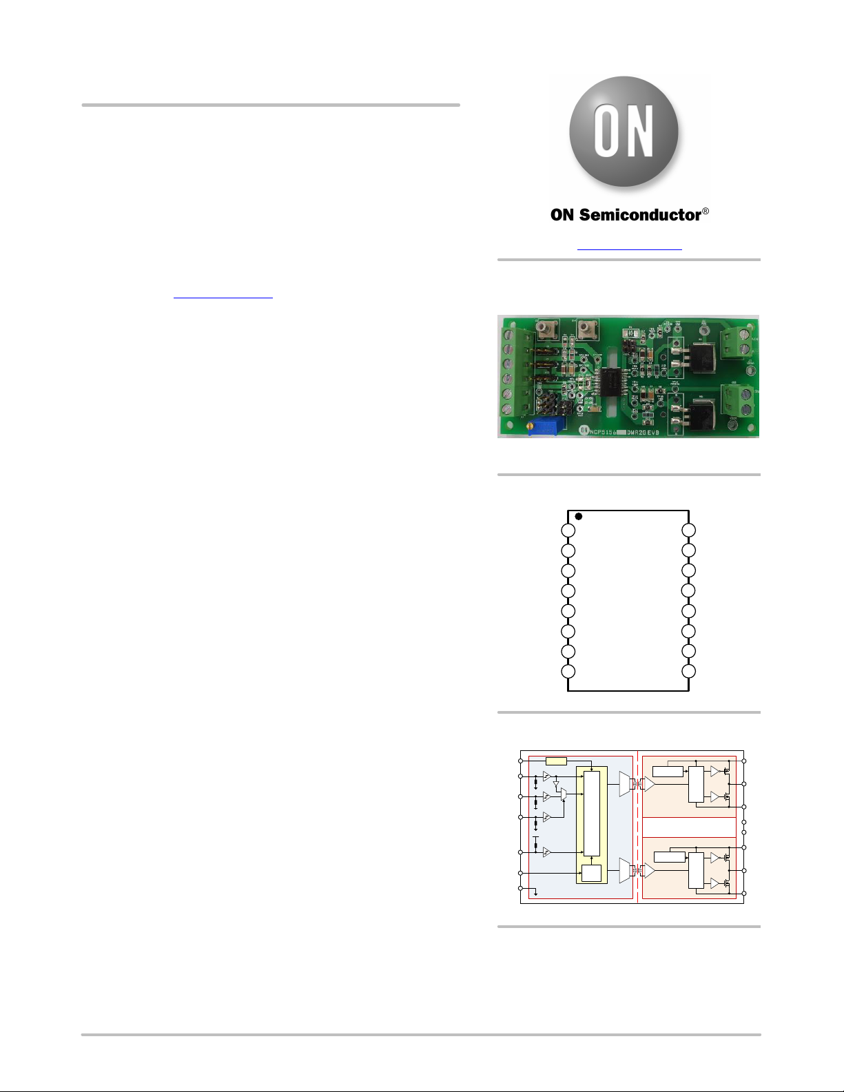
Figure 1. Evaluation Board Photo
MOSFET power switches. The NCP51561 offers short and matched
propagation delays.
Two independent and 5 kV
galvanically isolated gate driver
RMS
channels can be used in any possible configuration of two low−side,
two high−side switches or a half−bridge driver with programmable
dead time. A Enable pin shutdown both outputs simultaneously when
is set low.
The NCP51561 offers other important protection functions such as
independent under−voltage lockout for both gate drivers and enable
function.
Key Features
• Flexible: Dual Low−Side, Dual High−Side or Half−Bridge Gate
Driver
• Independent UVLO Protections for Both Output Drivers
• Output Supply Voltage from 9.5 V to 30 V with 8 V for MOSFET,
17 V UVLO for SiC, Thresholds
• 4.5 A Peak Source, 9 A Peak Sink Output Current Capability
• Common Mode Transient Immunity CMTI > 200 V/ns
• Propagation Delay Typical 36 ns with
♦ 8 ns Max Delay Matching per channel
♦ 8 ns Max Pulse−Width Distortion
• User Programmable Input Logic
♦ Single or Dual−input modes via ANB
♦ ENABLE or DISABLE Mode
• User Programmable Dead−Time
FUNCTIONAL BLOCK DIAGRAM
V
DD
INA
INB
ANB
NA/DIS
DT
GND
• Isolation & Safety
♦ 5 kV
Galvanic Isolation from Input to each Output and
RMS
1500 V Peak Differential Voltage between Output Channels
(per UL1577 Requirements)
♦ 1200 V Working Voltage (per VDE0884−11 Requirements)
www.onsemi.com
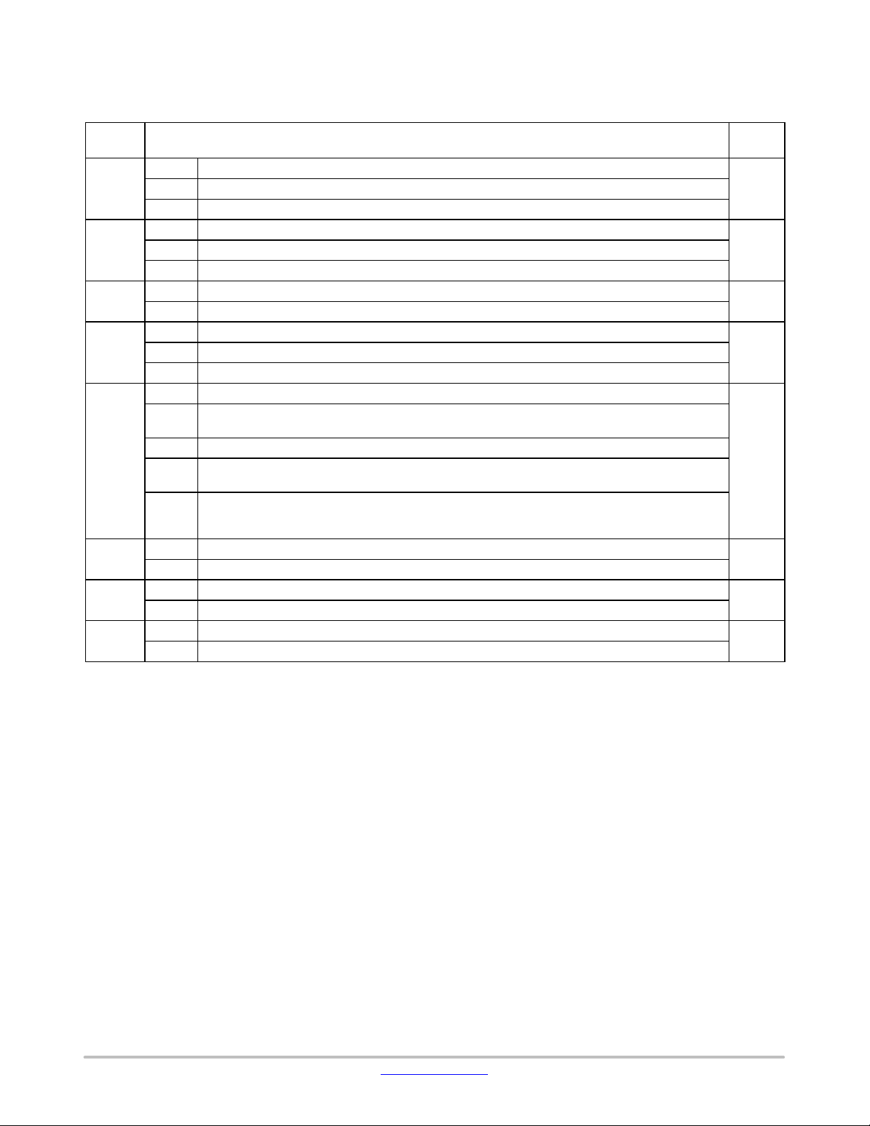
PIN CONNECTIONS
1
INA
2
INB
3
V
DD
4
GND
5
ENA/DIS
DT
6
ANB
7
8
V
DD
VDD UVLO
INA
INB
LOGIC
DEAD
TIME
CONTROL
INA
INB
Tx Rx
Tx
VCCA
OUTA
VSSA
VCCB
OUTB
VSSB
Isolation
Input to Output
Rx
UVLO
[5V, 8V, 17V]
UVLO
[5V, 8V, 17V]
NC
NC
16
15
14
13
12
11
10
9
Functional
Isolation
VCC
LOGIC
LOGIC
OUT
VSS
NC
NC
VCC
OUT
VSS
© Semiconductor Components Industries, LLC, 2020
March, 2021 − Rev. 1
1 Publication Order Number:
EVBUM2771/D
Page 2

NCP51561 EVBUM
EVALUATION BOARD OPERATION
This section describes how to operate the NCP51561
evaluation board (EVB). Make external connections to the
NCP51561 EVB using either the installed test−points or by
installing wires into the connectors. The main connections
that must be made to the EVB are the analog supply voltage,
input signal, and output load and monitoring equipment.
Features
• Evaluation board for the NCP5156x product family in a
wide body SOIC−16 package
• 3 V to 5.0 V VDD power supply range, and up to 30 V
VCCA/VCCB power supply range
• 4.5 A and 9 A source/sink current driving capability
• 5 kV
Isolation for 1 minute per UL 1577
RMS
• TTL −compatible inputs
• Allowable input voltage up to 18 V with for INA, INB,
and ANB pins
• Onboard trimmer potentiometer for dead−time
programming
• 3−position header with for INA, INB, ENA/DIS and
DT
• 2−position header with for ANB
• Support for half−bridge test with MOSFETs, IGBTs
and SiC MOSFETs with connection to external power
stage
Power and Ground
NOTE: Connecting the all power supplies in reverse
polarity (backwards) will instantly device when
power is turned on and device damage can
result.
The primary side of the EVM (V
3 V to 5.0 V power supply and connected via J2. T est point
DD) operates from a single
(TP6 and TP7) is available for monitoring the primary
power supply.
The EVM provides connections for evaluating the output
side (V
CCA, VSSA, VCCB, and VSSB) power supplies for the
channel A and B, from a minimum 9.5 V to maximum 30 V
for 8 V UVLO version as shown in Figure 4. V
CCA and VCCB
can be monitored via TP9 and TP13, respectively.
The V
CCA and VCCB pin should be bypassed with a
capacitor with a value of at least ten times the gate
capacitance, and over 100 nF and located as close to the
device as possible for the purpose of decoupling. A low
ESR, ceramic surface mount capacitor is necessary. We had
recommends using 2 capacitors; a over 100 nF ceramic
surface−mount capacitor, and another a tantalium or
electrolytic capacitor of few microfarads added in parallel.
Input and Output
1. Connection of primary−side power supply to the
V
connector [J2].
DD
2. Connection of secondary−side power supply to the
V
CCA
and V
connector [J9, and J13].
CCB
3. Connection of INA signal to the SIGNAL
connector [J1−1, and J4].
4. Connection of INB signal to the SIGNAL
connector [J1−2, and J5].
5. Connection of ENABLE signal to the ENA/DIS
connector [J1−3, and J15].
6. Connection of ANB signal to the ANB jumper
[J11].
7. Connection of DC link power supply to the V
DC
connector [J6].
8. Connection of bridge output to the V
connector
SSA
[J7 and J12].
www.onsemi.com
2
Page 3
Evaluation Board Jumper Setting
Table 1. EVB JUMPER SETTING
Jumper
Jumper Setting Options
Default
Option1
Jumper not installed, INA/PWM signal provided by external signal and this pin is default low if left open
Option2
Jumper on J4−INA−2 and J4−INA−3 set INA low
Option3
Jumper on J4−INA−2 and J4−INA−1 set INA high
Option1
Jumper not installed, INB signal provided by external signal and this pin is default low if left open
Option2
Jumper on J5−INB−2 and J5−INB−3 set INB low
Option3
Jumper on J5−INB−2 and J5−INB−1 set INB high
Option1
Jumper on J11−ANB−2 and J11−ANB−4 set ANB low for dual input mode
1
Option2
Jumper on J11−ANB−1 and J11−ANB−3 set ANB high for single input (PWM) mode
Option1
Jumper not installed, DISABLE signal provided by external signal and this pin is default low if left open
Option2
Jumper on J15−ENA/DIS−2 and J15−ENA/DIS−3 set DISABLE low (Or ENABLE low)
Option3
Jumper on J15−ENA/DIS−2 and J15−ENA/DIS−1 set DISABLE high (Or ENABLE high)
Option1
Jumper not installed and R13 is open or below 1 kW, shoot−through prevention with 10−ns dead time
4
Option2
Jumper on J14−DT−1 and J14−DT−2 set DT VDD for allows driver both output overlap or driver output
Option3
Jumper on J14−DT−3 and J14−DT−4 set DT for fixed resistance for 20 kW.
Option4
Jumper not installed and R13 = 100 kW. It is recommended close to the DT pin to achieve better noise
Option5
Jumper on J14−DT−5 and J14−DT−6 set the dead time by DT (in ns) = R
(in kW) × 10. For better
Option1
Jumper on T.P1−1 and T.P1−2 for half−bridge application
Option2
Jumper off T.P1−1 and T.P1−2 for bench test.
Option1
Jumper on T.P2−1 and T.P2−2 and jumper on J16−2 and J16−4 for single power supply (VCCA=VCCB)
Option2
Jumper on T.P2−1 and T.P2−2 and and jumper on J16−1 and J16−3 for VCCA bootstrap supply
Option1
Jumper on T.P3−1 and T.P3−2 for single power supply (e.g. VSSA=VSSB)
Option2
Jumper off T.P3−1 and T.P3−2 for dual power supply
J4−INA
NCP51561 EVBUM
Setting
Option1
J5−INB
J11−ANB
J15−EN
A/DIS
J14_DT
T.P1
T.P2
T.P3
Option1
Option
Option2
Option
follow input signals (INA & INB)
immunity.
DT
noise immunity and dead−time matching, We recommends to parallel a 2.2−nF or above bypassing
capacitor from DT pin to GND.
Option2
Option1
Option1
Evaluation Board Setting before Power Up
1. If the ENABLE function is used, ENA/DIS pin
(PIN5) should be connected to VDD (PIN3 or
PIN8) through a wire−bridge between pin 1 and
In addition, Cross−conduction between both driver
outputs (OUTA, and OUTB) is not allowed with
minimum dead time (t
the DT pin is floating (Open).
pin 2 of J15 or this pin is default HIGH if left
open.
On the other hand, if using the Disable mode ,
should be connect ENA/DIS pin to GND pin
through a wire−bridge between pin 2 and pin 3 of
J15.
2. If using the dual input mode, should be ANB pin
(PIN7) connected to GND (PIN4) through a
wire−bridge between pin 2 and pin 4 of J11 or this
pin is default low if left open.
On the other hand, if using the single input mode,
should be connect ANB pin to VDD pin through a
wire−bridge between pin 1 and pin 3 of J11.
3. Should be connect to the resistance between DT
pin (pin6) and GND (pin4) for dead−time control
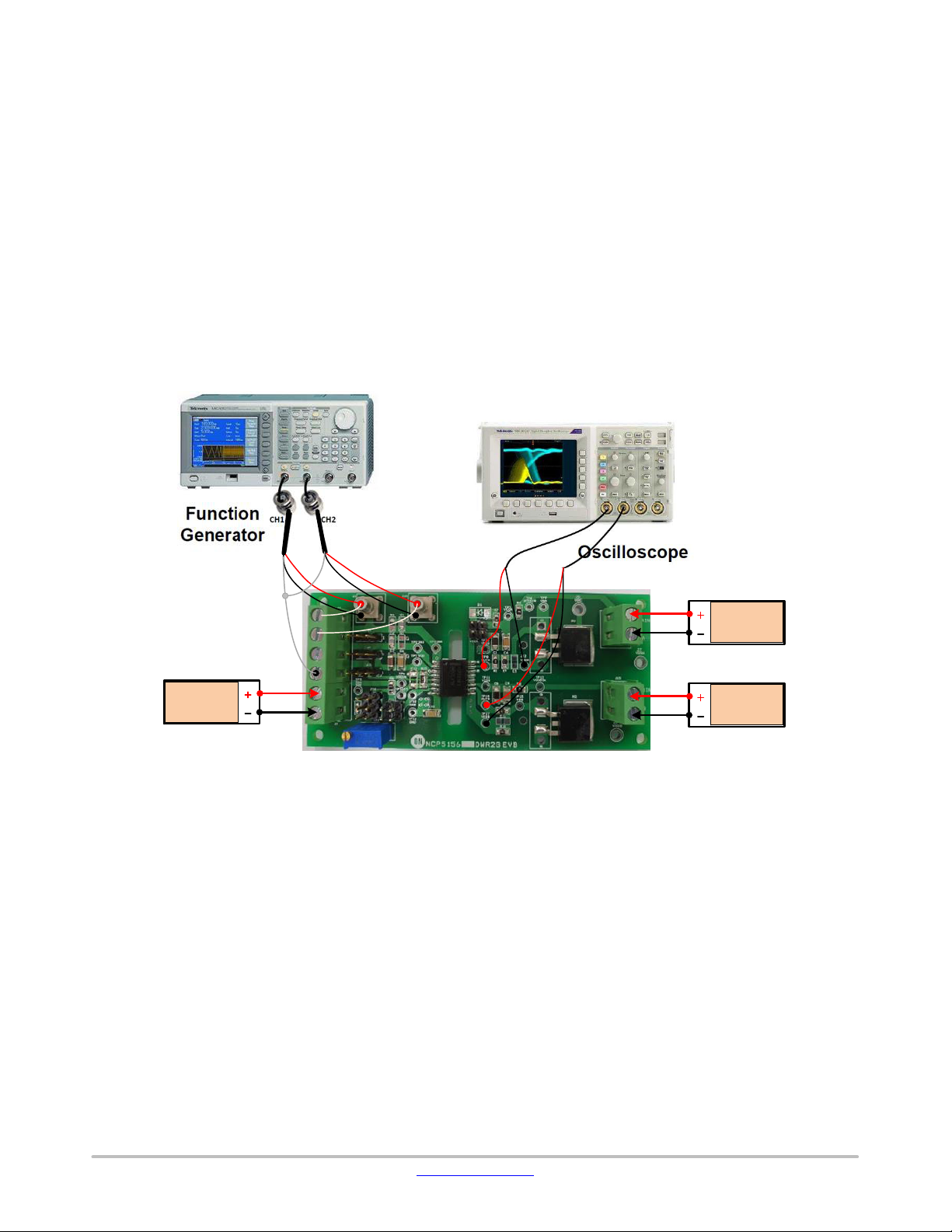
Bench Setup
The bench setup diagram includes the function generator,
power supplies and oscilloscope connections.
Follow the connection procedure below and use Figure 2
as a reference
• Make sure all the output of the function generator,
power supplies are disabled before connection
• Function generator channel−A channel applied on INA
(J3 or J1 pin−1) ↔ TP1 as seen in Figure 2.
• Function generator channel−B channel applied on INB
(J10 or J1 pin−2) ↔ TP2 as seen in Figure 2.
• If the ENABLE function is not used, ENA/DIS pin
(PIN5) should be connected to VDD (PIN3 or PIN8)
mode.
www.onsemi.com
3
DTMIN) typically 10 ns when
Page 4
NCP51561 EVBUM
through a wire−bridge between pin 1 and pin 2 of J15
or this pin is default HIGH if left open.
• If using the dual input signals (INA and INB) with
same polarity, should be DT pin (PIN6) connected to
VDD (PIN3 or 8) through a wire−bridge between pin 1
and pin 2 of J14.
On the other hand, if using the dual input signals with
opposite polarity, should be connect to the resistance
(R13) between DT pin (pin6) and GND (pin4) or DT
pin is floating (Open).
• If using the dual input mode, should be ANB pin
(PIN7) connected to GND (PIN4) through a
wire−bridge between pin 2 and pin 4 of J11 or this pin
is default low if left open.
On the other hand, if using the single input mode,
should be connect ANB pin to VDD pin through a
wire−bridge between pin 1 and pin 3 of J11.
• Power supply #1: positive node applied on J2 pin−1 (or
TP6), and negative node applied on J2 pin−2.
• Power supply #2: positive node applied on J9 pin−1(or
TP14), negative node connected directly to J9 pin−2 (or
TP10) and should be connected to VAIN and VCCA
through a wire−bridge between pin 2 and pin 4 of J16.
• Power supply #3: positive node applied on J13 pin−1
(or TP13), negative node connected directly to J13
pin−2 (or TP17)
• Oscilloscope channel−A probes TP8 ↔ TP10, smaller
measurement loop is preferred
• Oscilloscope channel−B probes TP14 ↔ TP17, smaller
measurement loop is preferred
POWER
SUPPLY #1
(5V/0.05A)
Figure 2. Bench Setup Diagram and Configuration
POWER
SUPPLY #2
(12V/0.1A)
POWER
SUPPLY #3
(12V/0.1A)
www.onsemi.com
4
Page 5
Power Up and Power Down Procedure
Power Up
1. Could be connect VSSA pin to VSSB pin through
a wire−bridge between pin 1 and pin 2 of T.P3, if
the Half−Bridge application is not used.
2. Enable power supply through pin1 of J2 VDD
connector in primary−side
3. Enable power supply through pin1 of J9 VCCA
connector and through pin1 of J13 VCCB
connector in secondary−side
Measure the quiescent current of VCCA, and
VCCB on DMM1 and DMM2 ranges from 0.5 mA
to approximately 1.0 mA if everything is set
correctly;
NCP51561 EVBUM
4. Enable the function generator, two−channel
outputs: channel−A and channel−B;
5. There will be:
A. Stable pulse output on the channel−A and
channel−B in the oscilloscope
B. Scope frequency measurement is the same with
function generator output;
C. DMM #1 and #2 read measurement results
should be around 2.5 mA ± 1 mA under no load
conditions. For more information about operating
current, refer to the NCP51561 data sheet.
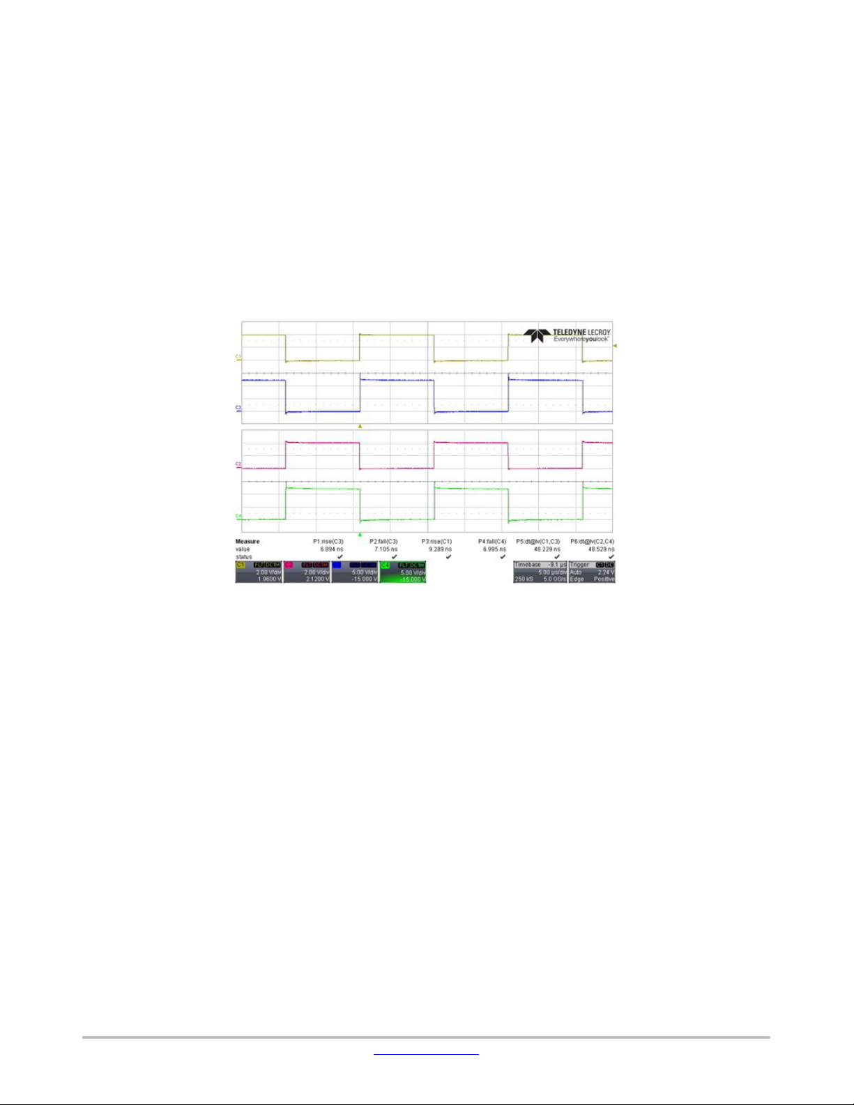
CH1: INA, CH2: INB, CH3: OUTA, and CH4: OUTB
Figure 3. Experimental Waveforms of Input to Output
Power Down
1. Disable function generator
2. Disable power supply of VCCA, and VCCB in
secondary−side
3. Disable power supply of VDD in primary−side
4. Disconnect cables and probes
www.onsemi.com
5
Page 6

NCP51561 EVBUM
Table 2. LIST OF TEST POINT
TP
Reference
Description
TP1
INA
Logic Input for Channel A with internal pull−down resistor to GND.
TP2
INB
Logic Input for Channel B with internal pull−down resistor to GND.
TP3
VCCA
TP4
VCCAIN
TP5
ENA/DIS
Logic Input High enables both output channels. Internal pull−up resistor
TP6
VDDIN
TP7
VDD
TP8
OUTA
TP9
VGA
TP10
VSSA
Ground for Channel A
TP11
VCCB
Supply Voltage for Output Channel B.
TP12
GND
Ground Input−side. (all signals on input−side are referenced to this pin)
TP13
VCCBIN
Supply Voltage for Output Channel B.
TP14
OUTB
TP15
VGB
TP16
DT
Input for programmable Dead−Time
TP17
VSSB
Ground for Channel B
TP18
ANB
Logic Input for changing the input signal configuration with internal pull−down resistor to GND. The OUTA
l
Figure 4 shows an application schematic of NCP51561 for
an evaluation board.
TP7
J4
1
J10
PWMA
PWMB
ENA
GND
VDD
GND
J3
2
J1
J2
3
1
J5
2
1
3
2
4
3
J15
1
2
3
TP6
R6
0
1
2
R12
20k
J11
1
2
J14
1
3
5
R11
500k
2.2nF
C12
TP1
C1
R1
DNP
10pF
51
C2
R3
DNP
10pF
51
C7
C6
0.22uF
10uF
TP5
3
4
2
4
6
DNP
TP16
TP18
R13
100k
C10
0.22uF
U1
TP2
1
INA
2
INB
3
V
DD
4
GND
5
ENA/DIS
6
DT
ANB
7
8
V
DD
NCP51561
VCCA
OUTA
VSSA
NC
NC
VCCB
OUTB
VSSB
VAIN
J6
VDC
TP4
M1
R7
10k
J9
1
VCCA
VSSA
TP3
J16
D1
3
4
VCCA
16
15
0.22uF
C3
R5
4.7
R2
1
DNP
2
US1MFA
10
TP9
R4
VAIN
0
C4
10uF
C5
DNP
1 nF
14
T.P1
J7
VSSA
J12
VSSA
J13
1
VCCB
2
VSSB
J8
VSSB
0.22uF
TP10
T.P2
VCCBVAIN
12
T.P3
VSSBVSSA
12
TP13
DNP
TP15
C11
1 nF
R8
0
C9
C8
10uF
R9
4.7
12
M2
R10
10k
TP8
13
12
TP11
VCCB
11
10
9
TP17
TP14
Figure 4. Typical Application Schematic of NCP51561 EVB
List of Test Point
Table 2 show the test point list of NCP51561 for an
evaluation board.
Supply Voltage for Output Channel A.
It is recommended to place a bypass capacitor from VCCA to VSSA.
Input−side Supply Voltage.
It is recommended to place a bypass capacitor from VDD to GND.
Output for Channel A
It is recommended to place a bypass capacitor from VCCB to VSSB.
Output for Channel B
and OUTB as complementary outputs from one PWM input signal on the INA pin regardless the INB signa
when the ANB pin is high. The INB pin should be pulled down to GND (recommended) or floating (not recommended) when the ANB pin is high. The ANB pin should be kept low when INA and INB pins control the
OUTA and OUTB individually.
www.onsemi.com
6
Page 7

NCP51561 EVBUM
Table 3. ELECTRICAL SPECIFICATIONS
Rating
Symbol
Min
Max
Unit
Power Supply Voltage – Input side
VDD3.0
5.0
V
V
V
Logic Input Voltage at pins INA, INB, and ANB
VIN018V
Logic Input Voltage at pin ENA/DIS
V
0
5.0
V
Table 4. BILL OF MATERIAL
Reference
Qty
Description
Value
Footprint
Manufacturer
U11Gate driver
NCP51561
16 SOIC−WB
ON Semiconductor
D10Diode
US1MFA
SOD−123FL
ON Semiconductor
R1, R3
0
Resistors
5.1
SMD 2012
R21Resistors
2.2
SMD 2012
R4,R6, R83Resistors
0
SMD 2012
R5 ,R92Resistor
4.7
SMD 2012
R7, R102Resistor
10 k
SMD 2012
R11
1
Variable Resistor
500 k
R121Resistor
20 k
SMD 2012
R131Resistor
100 k
SMD 3216
C1, C2
2
Capacitor, Ceramic
10 pF, 50 V
SMD 2012
C3 , C6, C8, C10
4
Capacitor, Ceramic
0.22 uF, 50 V
SMD 3216
C7
3
Capacitor, Ceramic
10 uF, 16 V
SMD 3216
C4, C9
2
Capacitor, Ceramic
10 uF, 50 V
SMD 3216
C5, C11
2
Capacitor, Ceramic
1 nF, 50 V
SMD 2012
C12
1
Capacitor, Ceramic
2.2 nF, 50 V
SMD 3216
M1, M22TBD
J11Connector
EB21A−04−D
Adam Tech
J2,J9, J13
3
Connector
EB21A−02−D
Adam Tech
J3, J10
2
BNC Connector
SMB
J4, J5, J15
3
Header 3
J11, J16
2
Header 2 × 2
J141Header 3 × 2
J6,J7,J8, J12
2
Connector
Electrical Specifications
Table 3 shows the recommended operating conditions of
NCP51561 for the evaluation board.
Power Supply Voltage – Driver side
Operating Junction Temperature Tj −40
8−V UVLO Version
17−V UVLO Version 18 30
V
CCA
, V
ENA/DIS
CCB
Bill of Material (BOM)
Table 4 shows the bill of material (BOM) of NCP51561
for the evaluation board.
W
W
W
W
W
W
W
W
9.5 30
+150
°C
www.onsemi.com
7
Page 8

NCP51561 EVBUM
Input Stage
The input pins of NCP51561 is based on a TTL
compatible input−threshold logic that is independent of the
V
supply voltage for INA, INB, ANB, and ENA/DIS
DD
pins.
The logic level compatible input provides a typically high
threshold of 1.6 V and a typically low threshold of 1.1 V. The
input impedance of the NCP51561 is 200 kW typically, as
shown in Figure 5.
V
DD
TP1
INA
TP2
INB
TP5
ENA/DIS
J4
J5
J15
And we recommends an RC network is to be added on the
PWM input pins, INA and INB, for reducing the impact of
system noise and ground bounce, for example, 51 W (R1,
and R3) with 10 pF (C1, and C2) is an acceptable choice as
shown in Figure 5.
INA, INB, ENA/DIS and ANB
signal can be monitored
via TP1, TP2, TP5 and TP18, respectively.
INA
1
R1
R3
C7
C8
C2
C1
2
3
4
5
INB
V
GND
ENA/DIS
200 k
200 k
DD
200 k
Figure 5. Recommended Input Circuit
Output Stage
The output stage is able to sink/source typically around
4.5 A/9 A at 25°C for the NCP51561.
The EVB comes populated with a 1−nF load (C5, and
C11) on the output side. The OUTA and OUTB can be
monitored directly via TP8 and TP14, respectively.
The EVB also allows for evaluation of the device with an
MOSFET load in either of the standard TO−220, TO−3P,
TP18
J11
ANB
7
200 k
TO−247, and TO−252 (D−PAK), and TO−263 (D2PAK )
footprints. During evaluation with an MOSFET load, the
pre−installed capacitive load (C5 and C11) can be
disconnected from the each output.
The EVB provides an additional connection (J6) for
applying an external power supply to the MOSFET Drain.
The EVB is not intended for high voltage testing and the
voltage applied to J6 should be limited to 50 V DC.
www.onsemi.com
8
Page 9

NCP51561 EVBUM
PERFORMANCE OF EVALUATION BOARD
This section describes application guidance and operation
of the NCP51561 for an evaluation board (EVB) include key
functions.
Input Signal Configuration
The NCP51561 allows changing the input signal pin
configuration by the ANB pin for user convenience. (e.g.
single input – dual output, or dual input – dual output).
(a) INB = OPEN (LOW) with DT = Open
CH1: INA, CH2: ANB, CH3: OUTA, and CH4: OUTB
Figure 6. Experimental Waveforms of ANB Function with Dead−time
ANB Function
The NCP51561 allows changing the input signal pin
configuration by the ANB pin for user convenience. There
are two operating modes that allow changing the
configuration of the input to output channels (e.g. single
input – dual output, or dual input – dual output).
Figure 6 and Figure 7 shows the experimental result of
ANB function with and without dead−time control.
(b) INB = OPEN (LOW) with R
= 100 kW
DT
(a) INB = HIGH with DT = Open (b) INB = HIGH with DT = VDD
CH1: INA, CH2: ANB, CH3: OUTA, and CH4: OUTB
Figure 7. Experimental Waveforms of ANB Function
www.onsemi.com
9
Page 10

NCP51561 EVBUM
Protection Function
NCP51561 provide the protection features include Enable
function, and Under−Voltage Lockout (UVLO) of power
supplies in primary−side (V
channels (V
(INB)
OUTA
(OUTB)
Protection
Status
ENABLE
INA
CCA
, and V
CCB
), and secondary−side both
DD
).
Figure 8. Timing Chart of Enable Function
t1
Figure 9 shows an experimental result of enable function
that the ENA/DIS pin voltage goes to LOW state in normal
Enable Function
Figure 8 shows the timing chart of enable function. If the
ENA/DIS pin voltage goes to LOW state in normal
operation, the gate driver enters the shutdown (disable)
mode.
External Shutdown
t2
operation, the both driver output is turned−off immediately
even though input signals, INA and INB, are HIGH state.
CH1: INA and INB, CH2: ENA/DIS, CH3: OUTA, and CH4: OUTB
Figure 9. Experimental Waveforms of Enable Function
www.onsemi.com
10
Page 11

NCP51561 EVBUM
Under−Voltage Lockout Protection VDD
The NCP51561 provides the Under−Voltage Lockout
(UVLO) protection function for VDD in primary−side as
shown in Figure 10. The OUTA and OUTB as
CH1: INA, CH2: VDD, CH3: OUTA, and CH4: OUTB
complementary outputs from one PWM input signal on the
INA pin regardless the INB signal when the ANB pin is high.
As test result, the VDD UVLO turn−on and off threshold
voltages are around 2.8 V and 2.7 V respectively.
Figure 10. Experimental Waveforms of VDD Under−Voltage Lockout Protection
Under−Voltage Lockout Protection VCCx (VCCA and
VCCB)
The NCP51561 provides the Under−Voltage Lockout
(UVLO) protection function for both gate drive output for
VCCA and VCCB for 8 V version in secondary−side as
shown in Figure 11. The OUTA and OUTB as
complementary outputs from one PWM input signal on the
INA pin regardless the INB signal when the ANB pin is high.
As test result, the VCC UVLO turn−on and off threshold
voltages are around 8.7 V and 8.2 V respectively.
CH1: INA, CH2: VCCA, and VCCB, CH3: OUTA, and CH4: OUTB
Figure 11. Experimental Waveforms of VCC Under−Voltage Lockout Protection
www.onsemi.com
11
Page 12

NCP51561 EVBUM
Experimental Waveforms with Different DT
Configurations
This section shows experimental test results of dead−time
control with different DT configuration.
DT Pin Floating or Left Open
(J14−DT Option 1 in Table 1)
The dead−time(DT) between the outputs (OUTA and
OUTB) of the two channels is typically around 10 ns, which
is preset for shoot−through prevention as shown in
Figure 12.
CH1: INA, CH2: INB, CH3: OUTA, and CH4: OUTB
Figure 12. Experimental Waveforms if DT is left Open
DT Pin Connected to VDD (J14−DT Option 2 in Table 1)
Overlap is allowed both switches from conducting even
though at the same time when the DT pin pulled to VDD as
shown in Figure 13.
CH1: INA, CH2: INB, CH3: OUTA, and CH4: OUTB
Figure 13. Overlap is Allowed when DT Connected to VDD
www.onsemi.com
12
Page 13

NCP51561 EVBUM
DT Pin Connected to RDT (J14−DT Option 3 in Table 1)
Overlab is not allowed both switches at the same time
when the dead time (DT) control mode. The dead−time (DT)
between both outputs is set according to:
DT (in ns) = 10 × R
(in kW).
DT
CH1: INA, CH2: INB, CH3: OUTA, and CH4: OUTB
Figure 14. Experimental Waveforms if DT Connected to R
Figure shown the experimental results when the
dead−time control resistance for 100 kW.
DT
Dead Time Characteristics
Figure 15 shows the dead time characteristics and
operating modes according to the dead−time resistance
values of the NCP51561.
tDT [ns]
5000
4500
4000
3500
3000
2500
2000
1500
1000
500
0
Minimum Dead−time
MODE A – DT pin Open
t
=
10 ns
DT
Cross−conduction prevention active
1 50 100 150
Figure 15. Dead Time (DT vd. RDT)
Dead−time Control Range
MODE B – 1 k <R
t
[ns]=10⋅ RDT[k ]
DT
Cross−conduction prevention active
200
Output Overlap ENABLED
MODE C – DT pin pull to V
tDT=
0 ns
Cross−conduction prevention disabled
<500 k
W
W
R
DT
W
DT
250 300 500350 400 450
[k ]
W
DD
www.onsemi.com
13
Page 14

NCP51561 EVBUM
Output Driving Current Capability
Figure 16 shows the experimental result of source and
sink peak currents driving capability around 4.5 A and 10 A
(a) Source Current Capability (b) Sink Current Capability
CH1: INPUT, and CH2: OUTPUT Current
Figure 16. Experimental Waveforms of Current Driving Capability
ESD Structure
Figure 17 shows the multiple diodes related to an ESD
protection components of NCP51561. This illustrates the
absolute maximum rating for the device.
respectively at 25°C when the supply voltage (VCCA and
VCCB) is applied 12 V.
INA
INB
ENA/DIS
ANB
DT
VCCAVDD
3,8
1
2
5
7
6
20 V
5.5 V
33 V
33 V
4 9
16
15
OUTA
14
VSSA
11
VCCB
10
OUTB
GND
Figure 17. ESD Structure
www.onsemi.com
14
Page 15

NCP51561 EVBUM
VSSA
VSSB
Printed Circuit Board
Figure 18 shows the photograph of NCP51561 evaluation board.
.
INA
INB
EN
GND
V
DD
NCP51561
GND
Figure 18. Evaluation Board Picture (Top View)
Figure 19 shows the printed circuit board layout of
NCP51561 evaluation board.
V
CCA
V
CCB
(a) Top & Bottom View
(b) Top View
(c) Bottom View
Figure 19. Printed Circuit Board
www.onsemi.com
15
Page 16

ON Semiconductor and the ON Semiconductor logo are trademarks of Semiconductor Components Industries, LLC dba ON Semiconductor or its subsidiaries in the United States and/or
other countries. ON Semiconductor owns the rights to a number of patents, trademarks, copyrights, trade secrets, and other intellectual property. A listing of ON Semiconductor’s
product/patent coverage may be accessed at www.onsemi.com/site/pdf/Patent−Marking.pdf
subject to all applicable copyright laws and is not for resale in any manner.
The evaluation board/kit (research and development board/kit) (hereinafter the “board”) is not a finished product and is as such not available for sale to consumers. The board is only intended
for research, development, demonstration and evaluation purposes and should as such only be used in laboratory/development areas by persons with an engineering/technical training
and familiar with the risks associated with handling electrical/mechanical components, systems and subsystems. This person assumes full responsibility/liability for proper and safe handling.
Any other use, resale or redistribution for any other purpose is strictly prohibited.
The board is delivered “AS IS” and without warranty of any kind including, but not limited to, that the board is production−worthy, that the functions contained in the board will meet your
requirements, or that the operation of the board will be uninterrupted or error free. ON Semiconductor expressly disclaims all warranties, express, implied or otherwise, including without
limitation, warranties of fitness for a particular purpose and non−infringement of intellectual property rights.
ON Semiconductor reserves the right to make changes without further notice to any board.
You are responsible for determining whether the board will be suitable for your intended use or application or will achieve your intended results. Prior to using or distributing any systems
that have been evaluated, designed or tested using the board, you agree to test and validate your design to confirm the functionality for your application. Any technical, applications or design
information or advice, quality characterization, reliability data or other services provided by ON Semiconductor shall not constitute any representation or warranty by ON Semiconductor,
and no additional obligations or liabilities shall arise from ON Semiconductor having provided such information or services.
The boards are not designed, intended, or authorized for use in life support systems, or any FDA Class 3 medical devices or medical devices with a similar or equivalent classification in
a foreign jurisdiction, or any devices intended for implantation in the human body. Should you purchase or use the board for any such unintended or unauthorized application, you shall
indemnify and hold ON Semiconductor and its officers, employees, subsidiaries, affiliates, and distributors harmless against all claims, costs, damages, and expenses, and reasonable
attorney fees arising out of, directly or indirectly, any claim of personal injury or death associated with such unintended or unauthorized use, even if such claim alleges that ON Semiconductor
was negligent regarding the design or manufacture of the board.
This evaluation board/kit does not fall within the scope of the European Union directives regarding electromagnetic compatibility, restricted substances (RoHS), recycling (WEEE), FCC,
CE or UL, and may not meet the technical requirements of these or other related directives.
FCC WARNING – This evaluation board/kit is intended for use for engineering development, demonstration, or evaluation purposes only and is not considered by ON Semiconductor to
be a finished end product fit for general consumer use. It may generate, use, or radiate radio frequency energy and has not been tested for compliance with the limits of computing devices
pursuant to part 15 of FCC rules, which are designed to provide reasonable protection against radio frequency interference. Operation of this equipment may cause interference with radio
communications, in which case the user shall be responsible, at its expense, to take whatever measures may be required to correct this interference.
ON Semiconductor does not convey any license under its patent rights nor the rights of others.
LIMITATIONS OF LIABILITY: ON Semiconductor shall not be liable for any special, consequential, incidental, indirect or punitive damages, including, but not limited to the costs of
requalification, delay, loss of profits or goodwill, arising out of or in connection with the board, even if ON Semiconductor is advised of the possibility of such damages. In no event shall
ON Semiconductor’s aggregate liability from any obligation arising out of or in connection with the board, under any theory of liability, exceed the purchase price paid for the board, if any.
For more information and documentation, please visit www.onsemi.com
.
. ON Semiconductor is an Equal Opportunity/Affirmative Action Employer. This literature is
PUBLICATION ORDERING INFORMATION
LITERATURE FULFILLMENT:
Email Requests to: orderlit@onsemi.com
ON Semiconductor Website: www.onsemi.com
TECHNICAL SUPPORT
North American Technical Support:
Voice Mail: 1 800−282−9855 Toll Free USA/Canada
Phone: 011 421 33 790 2910
Europe, Middle East and Africa Technical Support:
Phone: 00421 33 790 2910
For additional information, please contact your local Sales Representative
◊
www.onsemi.com
1
 Loading...