

Page 1
NCP51199, NCV51199
DDR 2-Amp Source / Sink
V
Termination Regulator
TT
The NCP/NCV51199 is a linear regulator designed to supply a
regulated V
termination voltage for DDR−2 and DDR−3 memory
TT
applications. The regulator is capable of actively sourcing and sinking
±2 A peak currents for DDR−2, and DDR−3 up to ±1.5 A while
regulating the V
termination voltage is regulated to track V
voltage divider resistors connected to the PV
output voltage to within ±10 mV. The output
TT
/ 2 by two external
DDQ
, GND, and V
CC
REF
pins.
The NCP/NCV51199 incorporates a high−speed differential
amplifier to provide ultra−fast response to line and load transients.
Other features include source/sink current limiting, soft−start and
on−chip thermal shutdown protection.
Features
• Supports DDR−2 V
• Stable with 10 mF Ceramic Capacitance on V
Termination to ±2 A, DDR−3 to ±1.5 A (peak)
TT
Output
TT
• Integrated Power MOSFETs
• High Accuracy V
Output at Full−Load
TT
• Fast Transient Response
• Built−in Soft−Start
• Shutdown for Standby or Suspend Mode
• Integrated Thermal and Current−Limit Protection
• NCV Prefix for Automotive and Other Applications Requiring
Unique Site and Control Change Requirements; AEC−Q100
Qualified and PPAP Capable
• These Devices are Pb−Free and are RoHS Compliant
Typical Applications
• SDRAM Termination Voltage for DDR−2 / DDR−3
• Motherboard, Notebook, and VGA Card Memory Termination
• Set Top Box, Digital TV, Printers
www.
onsemi.com
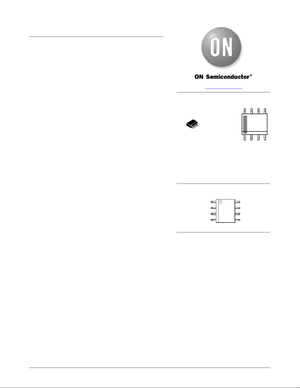
MARKING
DIAGRAM
8
1
NCPVCC
NC
V
NCV
CC
XXXXXX
ALYW
G
8
See detailed ordering, marking and shipping information in the
package dimensions section on page 6 of this data sheet.
SOIC8−NB EP
PD SUFFIX
CASE 751BU
1
XXXXXX = Specific Device Code
A = Assembly Location
L = Wafer Lot
Y = Year
WW = Work Week
G = Pb−Free Package
PIN CONNECTION
18
GND
VREF
TT
SOIC−8 EP
ORDERING INFORMATION
© Semiconductor Components Industries, LLC, 2017
April, 2017 − Rev. 3
1 Publication Order Number:
NCP51199/D
Page 2
= 1.5 to 5.0 V*
PV
CC
NCP51199, NCV51199
NCP51199
1
PV
CC
C2
6
V
CC
5 V
C3
Enable
R2
100k
R1
100k
C1
2
3
GND
V
REF
= 0.75 to 2.5 V*
V
C4
TT
R3
4
V
TT
*For DDR2: PVCC = 1.8 V, VTT = 0.9 V
DDR3: PV
= 1.5 V , VTT = 0.75 V
CC
C1 = 1 mF (Low ESR) C4 = 1000 mF + 10 mF (10 mF ceramic)
C2 = 470 mF (Low ESR) R3 = Optional V
discharge resistor
TT
C3 = 47 mF N−ch MOSFET = Optional Enable / Disable
Figure 1. Application Diagram
PIN FUNCTION DESCRIPTION
Pin No. Pin Name Description
1 PV
CC
2 GND Common Ground
3 V
4 V
REF
TT
5 NC True No Connect
6 V
CC
7 NC True No Connect
8 NC True No Connect
EP Thermal Pad Pad for thermal connection. The exposed pad must be connected to the ground plane using multiple
Input voltage which supplies current to the output pin. CIN = 470 mF with low ESR.
Buffered reference voltage input equal to ½ of V
divider dividing down the PV
(0.15 V maximum) turns the device off.
voltage creates the regulated output voltage. Pulling the pin to ground
CC
and active low shutdown pin. An external resistor
DDQ
Regulator output voltage capable of sourcing and sinking current while regulating the output rail.
= 1000 mF + 10 mF ceramic with low ESR.
C
OUT
The VCC pin is a 5 V input pin that provides internal bias to the controller. PVCC should always be kept
lower or equal to V
.
CC
vias for maximum power dissipation performance.
www.onsemi.com
2
Page 3
NCP51199, NCV51199
ABSOLUTE MAXIMUM RATINGS
Rating Symbol Value Unit
Input Supply Voltage Range (Vcc w PVCC) (Note 1) PVCC,
V
CC
Output Voltage Range V
Reference Input Range V
Maximum Junction Temperature T
TT
REF
J(max)
Storage Temperature Range TSTG −65 to 150 °C
ESD Capability, Human Body Model (Note 2) ESDHBM 2 kV
ESD Capability, Machine Model (Note 2) ESDMM 150 V
Lead Temperature Soldering
Reflow (SMD Styles Only), Pb−Free Versions (Note 3)
T
SLD
Stresses exceeding those listed in the Maximum Ratings table may damage the device. If any of these limits are exceeded, device functionality
should not be assumed, damage may occur and reliability may be affected.
1. Refer to ELECTRICAL CHARACTERISTICS and APPLICATION INFORMATION for Safe Operating Area.
2. This device series incorporates ESD protection and is tested by the following methods:
ESD Human Body Model tested per AEC−Q100−002 (EIA/JESD22−A114)
ESD Machine Model tested per AEC−Q100−003 (EIA/JESD22−A115)
Latchup Current Maximum Rating: ≤150 mA per JEDEC standard: JESD78
3. For information, please refer to our Soldering and Mounting Techniques Reference Manual, SOLDERRM/D
−0.3 to 6 V
−0.3 to 6 V
−0.3 to 6 V
125 °C
260 °C
THERMAL CHARACTERISTICS
Rating Symbol Value Unit
Thermal Characteristics, SO8−EP (Note 4)
Thermal Resistance, Junction−to−Air (Note 5)
Power Rating at 25°C Ambient = 1.19 W, derate 12 mW/°C
Thermal Reference, Junction−to−Lead2 (Note 5)
4. Refer to ELECTRICAL CHARACTERISTIS and APPLICATION INFORMATION for Safe Operating Area.
5. Values based on copper area of 645 mm
2
(or 1 in2) of 1 oz copper thickness and FR4 PCB substrate.
R
q
JA
R
Y
JL
OPERATING RANGES (Note 6)
Rating
Input Voltage PV
Bias Supply Voltage V
Ambient Temperature T
Junction Temperature T
6. Refer to ELECTRICAL CHARACTERISTICS and APPLICATION INFORMATION for Safe Operating Area.
Symbol Min Max Unit
CC
CC
A
J
1.5 5.5 V
4.75 5.25 V
−40 85 °C
−40 125 °C
84
°C/W
20
www.onsemi.com
3
Page 4

NCP51199, NCV51199
ELECTRICAL CHARACTERISTICS
PVCC = 1.8 V / 1.5 V; VCC = 5 V; V
Parameter Test Conditions Symbol Min Typ Max Unit
REGULATOR OUTPUT
Output Offset Voltage
Load Regulation V
INPUT AND STANDBY CURRENTS
Bias Supply Current
Standby Current
CURRENT LIMIT PROTECTION
Current Limit
SHUTDOWN THRESHOLDS
Shutdown Threshold Voltage
THERMAL SHUTDOWN
Thermal Shutdown Temperature
Thermal Shutdown Hysteresis V
= 0.9 V / 0.75 V; C
REF
= 900 mV, I
REF
V
= 750 mV, I
REF
V
< 0.2 V (Shutdown), R
REF
PVCC = 1.8 V, V
PVCC = 1.5 V, V
= 10 mF (Ceramic); TA = +25°C, unless otherwise noted.
OUT
I
= 0 A V
out
= ±1.8 A, PVCC = 1.8 V
out
= ±1.4 A, PVCC = 1.5 V
out
I
= 0 A I
out
= 180W
LOAD
= 0.9 V
REF
= 0.75 V 1.5 − 3.5
REF
Enable V
Shutdown V
VCC = 5 V T
= 5 V T
CC
Reg
I
OS
load
BIAS
STB
I
LIM
IH
IL
SD
SH
−20 − +20 mV
mV
−10 − +10
− 0.8 2.5 mA
− 1 90
mA
2.0 − 3.5
A
0.6 − −
− − 0.15
V
160 168 176 °C
35 35 40 °C
www.onsemi.com
4
Page 5

NCP51199, NCV51199
TYPICAL CHARACTERISTICS
0.915
0.910
0.905
0.900
0.895
0.890
OUTPUT VOLTAGE (V)
0.885
0.880
PVCC = 1.8 V, VCC = 5 V
TEMPERATURE (°C)
Figure 2. Output Voltage vs. Temperature
0.60
0.55
0.50
0.45
0.40
0.35
0.30
SHUTDOWN THRESHOLD (V)
0.25
0.20
VCC = 5 V
TEMPERATURE (°C)
Figure 4. Shutdown Threshold vs.
Temperature
Enabled
Shutdown
0.770
0.765
0.760
0.755
0.750
0.745
0.740
OUTPUT VOLTAGE (V)
0.735
1007550 125250−25−50
0.730
PVCC = 1.5 V, VCC = 5 V
1007550 125250−25−50
TEMPERATURE (°C)
Figure 3. Output Voltage vs. Temperature
1.2
PVCC = 1.8 V, VCC = 5 V
1.0
0.8
0.6
CURRENT (mA)
CC
V
0.4
100 1257550250−25−50
0.2
1007550 125250−25−50
TEMPERATURE (°C)
Figure 5. VCC Current vs. Temperature
3.0
PVCC = 1.8 V, VCC = 5 V
2.5
2.0
1.5
CURRENT (mA)
1.0
CC
PV
0.5
0
Figure 6. PV
TEMPERATURE (°C)
Current vs. Temperature
CC
SOURCE CURRENT LIMIT (A)
1007550 125250−25−50
www.onsemi.com
5
3.5
3.0
2.5
2.0
1.5
1.0
0.5
PVCC = 1.8 V, VCC = 5 V
= 1.5 V, VCC = 5 V
PV
CC
0
TEMPERATURE (°C)
1007550 125250−25−50
Figure 7. Source Current Limits vs.
Temperature
Page 6

NCP51199, NCV51199
TYPICAL CHARACTERISTICS
3.5
3.0
2.5
2.0
1.5
1.0
SINK CURRENT LIMIT (A)
0.5
0
PVCC = 1.8 V, VCC = 5 V
= 1.5 V, VCC = 5 V
PV
CC
TEMPERATURE (°C)
Figure 8. Sink Current Limits vs. Temperature
1007550 125250−25−50
20
15
10
5
0
−5
−10
, TRANSIENT RESPONSE (mV)
−15
TT
V
−20
TIME (100 msec / div)
Figure 9. 1.25 V, +1.6 A Transient Response
Table 1. ORDERING INFORMATION
Device Marking Package Shipping
NCP51199PDR2G 51199
NCV51199PDR2G* V51199
†For information on tape and reel specifications, including part orientation and tape sizes, please refer to our Tape and Reel Packaging
Specifications Brochure, BRD8011/D.
*NCV Prefix for Automotive and Other Applications Requiring Unique Site and Control Change Requirements; AEC−Q100 Qualified and PPAP
Capable.
SOIC−8
(Pb-Free)
2500 / Tape & Reel
†
www.onsemi.com
6
Page 7

MECHANICAL CASE OUTLINE
PACKAGE DIMENSIONS
8
1
SCALE 1:1
2X 4 TIPS
D
8
E E1
C0.20
1
B
NOTE 5
TOP VIEW
NOTE 4
C0.10
A
D
e
SIDE VIEW
A
NOTE 5
5
4
NOTE 7
F
2X
NOTE 4
b8X
0.25
2X
8X
C
G
C0.10
M
C
C0.10 A-B
SEATING
PLANE
D
A-B D
C0.10
L2
DETAIL A
B
B
SOIC8−NB EP
CASE 751BU
ISSUE E
F
L
DETAIL A
END VIEW
b1
c
c1
SECTION B−B
DATE 01 APR 2015
NOTES:
1. DIMENSIONING AND TOLERANCING PER ASME
Y14.5M, 1994.
2. CONTROLLING DIMENSION: MILLIMETERS.
NOTE 6
A1
SEATING
C
PLANE
h
b
3. DIMENSION b DOES NOT INCLUDE DAMBAR
PROTRUSION. ALLOWABLE PROTRUSION SHALL
BE 0.10mm IN EXCESS OF MAXIMUM MATERIAL
CONDITION.
4. DIMENSION D DOES NOT INCLUDE MOLD FLASH,
PROTRUSIONS, OR GATE BURRS. MOLD FLASH,
PROTRUSIONS, OR GATE BURRS SHALL NOT EXCEED 0.15mm PER SIDE. DIMENSION E DOES NOT
INCLUDE INTERLEAD FLASH OR PROTRUSION.
INTERLEAD FLASH OR PROTRUSION SHALL NOT
EXCEED 0.25mm PER SIDE. DIMENSIONS D AND E
ARE DETERMINED AT DATUM F.
5. DIMENSIONS A AND B ARE TO BE DETERMINED
AT DATUM F.
6. A1 IS DEFINED AS THE VERTICAL DISTANCE
FROM THE SEATING PLANE TO THE LOWEST
POINT ON THE PACKAGE BODY.
7. TAB CONTOUR MAY VARY MINIMALLY TO INCLUDE
TOOLING FEATURES.
MILLIMETERS
DIM MIN MAX
A 1.35 1.75
A1 0.00 0.10
b 0.31 0.51
b1 0.28 0.48
c 0.17 0.25
c1 0.17 0.23
D 4.90 BSC
E 6.00 BSC
E1 3.90 BSC
e 1.27 BSC
F 1.55 2.39
G 1.55 2.39
h 0.25 0.50
L 0.40 1.27
L2 0.25 BSC
BOTTOM VIEW
RECOMMENDED
SOLDERING FOOTPRINT*
2.60
2.60
8X
1.52
7.00
1
8X
1.27
PITCH
DIMENSION: MILLIMETERS
*For additional information on our Pb−Free strategy and soldering
details, please download the ON Semiconductor Soldering and
Mounting Techniques Reference Manual, SOLDERRM/D.
DOCUMENT NUMBER:
DESCRIPTION:
ON Semiconductor and are trademarks of Semiconductor Components Industries, LLC dba ON Semiconductor or its subsidiaries in the United States and/or other countries.
ON Semiconductor reserves the right to make changes without further notice to any products herein. ON Semiconductor makes no warranty, representation or guarantee regarding
the suitability of its products for any particular purpose, nor does ON Semiconductor assume any liability arising out of the application or use of any product or circuit, and specifically
disclaims any and all liability, including without limitation special, consequential or incidental damages. ON Semiconductor does not convey any license under its patent rights nor the
rights of others.
98AON66222E
SOIC8−NB EP
0.76
Electronic versions are uncontrolled except when accessed directly from the Document Repository.
Printed versions are uncontrolled except when stamped “CONTROLLED COPY” in red.
MARKING DIAGRAM*
8
XXXXXXXXX
ALYWX
G
1
XXXXX = Specific Device Code
A = Assembly Location
L = Wafer Lot
Y = Year
W = Work Week
G = Pb−Free Package
*This information is generic. Please refer
to device data sheet for actual part
marking. Pb−Free indicator, “G”, may
or not be present.
PAGE 1 OF 1
GENERIC
© Semiconductor Components Industries, LLC, 2019
www.onsemi.com
Page 8

ON Semiconductor and are trademarks of Semiconductor Components Industries, LLC dba ON Semiconductor or its subsidiaries in the United States and/or other countries.
ON Semiconductor owns the rights to a number of patents, trademarks, copyrights, trade secrets, and other intellectual property. A listing of ON Semiconductor’s product/patent
coverage may be accessed at www.onsemi.com/site/pdf/Patent−Marking.pdf
ON Semiconductor makes no warranty, representation or guarantee regarding the suitability of its products for any particular purpose, nor does ON Semiconductor assume any liability
arising out of the application or use of any product or circuit, and specifically disclaims any and all liability, including without limitation special, consequential or incidental damages.
Buyer is responsible for its products and applications using ON Semiconductor products, including compliance with all laws, regulations and safety requirements or standards,
regardless of any support or applications information provided by ON Semiconductor. “Typical” parameters which may be provided in ON Semiconductor data sheets and/or
specifications can and do vary in different applications and actual performance may vary over time. All operating parameters, including “Typicals” must be validated for each customer
application by customer’s technical experts. ON Semiconductor does not convey any license under its patent rights nor the rights of others. ON Semiconductor products are not
designed, intended, or authorized for use as a critical component in life support systems or any FDA Class 3 medical devices or medical devices with a same or similar classification
in a foreign jurisdiction or any devices intended for implantation in the human body. Should Buyer purchase or use ON Semiconductor products for any such unintended or unauthorized
application, Buyer shall indemnify and hold ON Semiconductor and its officers, employees, subsidiaries, affiliates, and distributors harmless against all claims, costs, damages, and
expenses, and reasonable attorney fees arising out of, directly or indirectly, any claim of personal injury or death associated with such unintended or unauthorized use, even if such
claim alleges that ON Semiconductor was negligent regarding the design or manufacture of the part. ON Semiconductor is an Equal Opportunity/Affirmative Action Employer. This
literature is subject to all applicable copyright laws and is not for resale in any manner.
. ON Semiconductor reserves the right to make changes without further notice to any products herein.
PUBLICATION ORDERING INFORMATION
LITERATURE FULFILLMENT:
Email Requests to: orderlit@onsemi.com
ON Semiconductor Website: www.onsemi.com
TECHNICAL SUPPORT
North American Technical Support:
Voice Mail: 1 800−282−9855 Toll Free USA/Canada
Phone: 011 421 33 790 2910
Europe, Middle East and Africa Technical Support:
Phone: 00421 33 790 2910
For additional information, please contact your local Sales Representative
◊
www.onsemi.com
1
 Loading...