

Page 1
NCP5106BA36WGEVB
NCP5106B 36W Ballast
Evaluation Board User's
Manual
http://onsemi.com
EVAL BOARD USER’S MANUAL
Introduction
This document describes how the NCP5106B driver can
be implemented in a ballast application. The scope of this
application note is to highlight the NCP5106B driver and not
to explain or detailed how to build electronic ballast.
The NCP5106B is a high voltage power MOSFET driver
providing two outputs for direct drive of 2 N−channel power
MOSFETs arranged in a half−bridge configuration with a
cross conduction protection between the 2 channels.
It uses the bootstrap technique to insure a proper drive of
the High−side power switch. The driver works with 2
independent inputs to accommodate any topology
(including half−bridge, asymmetrical half−bridge, active
clamp and full−bridge).
Evaluation Board Specification
• Input range : 85 − 145 Vac or 184 − 265 Vac
• Ballast Output power : 36 W (type PL−L 36W)
♦ Pre−Heating current : 295 mA
♦ Pre−heating time : 1 second
♦ Nominal current : 414 mA
BEFORE PLUGGING IN THE DEMO BOARD, MAKE
SURE THE JUMPER IS ON THE CORRECT POSITION:
IF J2 IS USED, THEN Vin MUST BE LOWER THAN
145 Vac.
Detailed Operation
The lamp ballast is powered via a half bridge
configuration. The 2 power MOSFETs are driven with the
NCP5106B driver. The driver is supplied by the VCC rail,
and the high side driver is supplied by the bootstrap diode:
when the low side power MOSFET (Q2) is switched ON, the
BRIDGE pin is pulled down to the ground, thus the capacitor
connected between BRIDGE pin and VBOOT pin is
refuelled via the diode D3 and the resistor R5 connected to
V
. When Q2 is switched OFF the bootstrap capacitor C6
CC
supplies the high side driver with a voltage equal to V
level minus the D3 forward voltage diode. Given the
NCP5106B architecture, it is up to the designer to generate
the right input signal polarity with the desired dead time.
Nevertheless the NCP5106B provides a cross conduction
protection with an internal fixed dead time. Thus in case of
overlap on the inputs signal, the both outputs driver will be
kept in low state, or a minimum of 100 ns dead time will be
applied between the both drivers.
The 555 timer generates only one signal for the driver, the
second one, in opposite phase is built by inserting a NPN
transistor (Q4) for inverting the signal. Afterwards the dead
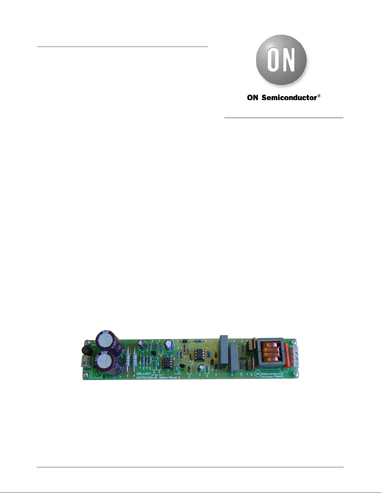
time is built with R2, D2 and C13 (typically 400 ns, see
Figure 2).
CC
© Semiconductor Components Industries, LLC, 2012
November, 2012 − Rev. 1
Figure 1. Evaluation Board Photo
1 Publication Order Number:
EVBUM2154/D
Page 2
NCP5106BA36WGEVB
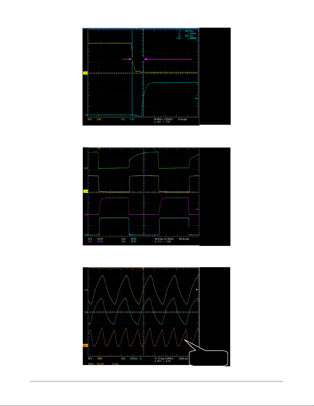
DRV_HI
Dead time 40 0 ns
Figure 2. Dead Time Between the High and Low Side Driver
(5 V/div)
DRV_LO
(5 V/div)
Time
(400 ns/div)
IN_HI
(10 V/div)
Figure 3. Input Output Timing Diagram
DRV_HI
(10 V/div)
IN_LO
(10 V/div)
DRV_LO
(10 V/div)
Time
(4 ms/div)
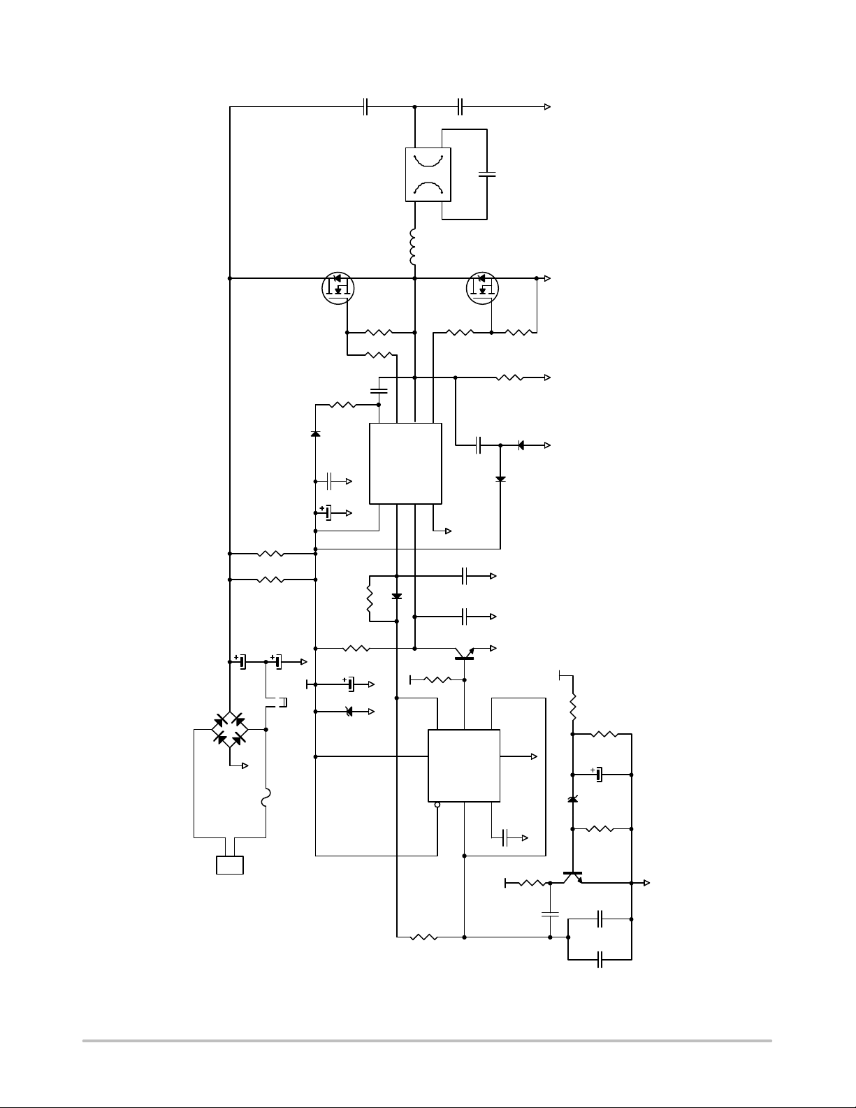
Tube
Voltage
(100 V /div)
Tube
current
(0.5 V/div)
Figure 4. Tube Signals
http://onsemi.com
2
Tube
Power
(50 W/div)
Tube average
power = 32 W
Page 3
NCP5106BA36WGEVB
C7
220nF
400V
B1
L1
Q1
IRF840LC
R8
10k
R6
10R
C6
100nF
R5
10R
D3
1N4936
C5
100nF
C4
4.7uF
R4
82k
2W
R3
82k
2W
C1
47 uF
400 V
SerieM Panasonic
C1
47 uF
400 V
SerieM Panasonic
1
1
PT1
4
J1
2
DF06
2
GND
F1
T500 mA
1
2
CON2
VCC
J2
3
US−jumper
R1
GND
C3
D1
7
8
VBOOT
VCC1IN_HI2IN_LO3GND
GND GND
110k
D2
R2
22k
220uF
15V
1.3W
GND GND
DRV_HI
6
BRIDGE
1N4148
VCC
U1
R10
1.4mH
5
DRV_LO
U2
4
R13
15k
3
Q
VCC8GND
R
TLC555C
4
33k
C8
220nF
400V
C15
BALLAST
R7
10R
C14
NCP5106B
GND
C13
18pF
C12
18pF
Q4
BC547B
7
DIS
TRIG
2
6.8nF
1kV
Q2
IRF840LC
R9
10k
R14
390k
D6
220pF/400V
D5
1N4936
GND GND
GND
6
THR
1
CVolt
5
C11
10nF
VCC
1N4936
GND
R11
47k
C9
GND
220pF
GND
GND
GND
GND
VCC
Q3
R12
D4
BC547B
27k
5V1
R16
C17
R15
C10
C16
68k
100 uF
22k
GND
220pF
NC
Figure 5. Evaluation Board Schematic
http://onsemi.com
3
Page 4

NCP5106BA36WGEVB
Figure 6. PCB Printout: Top and Bottom View
http://onsemi.com
4
Page 5

NCP5106BA36WGEVB
BILL OF MATERIALS
Designator Qty Description Value
B1 2 Connector 2/” - rad5.08mm Weidmuller PM5.08/2/90 Yes Yes
C1, C2 2 Electrolytic
C11 1 Capacitor 10 nF, 100 V 10% radial Murata RPER72A103K2M1B05A Ye s Yes
C12, C13 2 Capacitor 18 pF, 100 V 2% radial BC Comp. 2222-682-10189 Ye s Yes
C14 1 Capacitor 220 pF, 1000 V 10% radial Panasonic PICECKA3A221KBP Ye s Ye s
C15 1 Capacitor 6.8 nF, 1600 V 5% radial BC Comp. 2222 375 30682 Yes Yes
C16 1 Capacitor - - radial - - Yes Yes
C17 1 Electrolytic
C3 1 Electrolytic
C4 1 Electrolytic
C5, C6 2 Capacitor 100 nF, 50 V 10% radial Murata RPER71H104K2M1A05U Ye s Yes
C7, C8 2 Capacitor 220 nF, 400 V 10% radial Vishay MKT1822422405 Yes Yes
C9, C10 2 Capacitor 220 pF, 100 V 5% radial Murata RPE5C2A221J2M1Z05A Ye s Yes
D1 1 Zener Diode 15 V, 1.3 W 5% axial Vishay BZX85C15 Yes Yes
D2 1 High-Speed
D3, D5, D6 3 Rectifier Diode 1 A, 400 V 0% axial ON
D4 1 Zener Diode 5.1 V, 1.3 W 5% axial Vishay BZX85C5V1 Ye s Ye s
F1 1 Fuse 500 mA, 250 V 0% radial Schurter 0034-6612 Ye s Ye s
J1 1 Connector 2/” - rad5.08mm Weidmuller PM5.08/2/90 Ye s Ye s
J2 1 Resistor
L1 1 Inductor 1.4 mH - - Vogt 53-044 No Yes
PT1 1 Diode Bridge 600 V, 1 A 0% dil General
Q1, Q2 2 Power MOSFET
Q3, Q4 2 NPN Transistor 100 mA, 45 V - to92 ON
R1, R15 1 Resistor
R10 1 Resistor
R11 1 Resistor
R12 1 Resistor
R13 1 Resistor
R14 1 Resistor
R16 1 Resistor
R2 1 Resistor
R3, R4 2 Resistor
R5, R6, R7 3 Resistor
R8, R9 2 Resistor
U1 1 CMOS IC analog/timer - dip8 Texas
U2 1 NCP5106B NCP5106B - dip8 ON
Capacitor
Capacitor
Capacitor
Capacitor
Diode
N-Channel
47 uF, 400 V 20% radial Panasonic ECA2GM470 Yes Yes
100 uF, 16 V 20% radial Panasonic ECA1CM101 Yes Ye s
220 uF, 16 V 20% radial BC Comp. 2222-13555221 Yes Yes
4.7 uF, 63 V 20% radial Nippon
0.2 A, 75 V 0% axial Philips
0 W, 0.25 W
8 A, 500 V - to220 International
22 kW, 0.33 W
33 kW, 0.33 W
47 kW, 0.33 W
27 kW, 0.33 W
15 kW, 0.33 W
390 kW, 0.33 W
68 kW, 0.33 W
120 kW, 0.33 W
82 kW, 3 W
10 W, 0.33 W
10 kW, 0.33 W
Toler-
ance
Footprint Manufacturer
Chemi-Con
Semiconductor
Semiconductor
0% axial Multicomp MCF0.25W0R Ye s Ye s
Semiconductor
Rectifier
Semiconductor
5% axial Neohm CFR25J22K Yes Yes
5% axial Neohm CFR25J33K Yes Yes
5% axial Neohm CFR25J45K Yes Yes
5% axial Neohm CFR25J27K Yes Yes
5% axial Neohm CFR25J15K Yes Yes
5% axial Neohm CFR25J390K Yes Yes
5% axial Neohm CFR25J68K Yes Yes
5% axial Neohm CFR25J120K Yes Yes
5% axial BC Comp. 232219514823 Ye s Yes
5% axial Neohm CFR25J10R Ye s Ye s
5% axial Neohm CFR25J10K Yes Yes
Instruments
Semiconductor
Manufacturer Part
Number
SMEVB4.7UF63V Yes Yes
1N4148 Ye s Yes
1N4936G Yes Yes
DF06M Yes Ye s
INF840LC Ye s Ye s
BC547B Ye s Ye s
TLC555CP No Ye s
NCP5106B No Yes
Substi-
tution
Allowed
Lead
Free
http://onsemi.com
5
Page 6

NCP5106BA36WGEVB
TEST PROCEDURE FOR THE NCP5106B EVALUATION BOARD
A
Vac
Required Equipment
V
J2 jumper
Figure 7. Test Setup
• AC power source can be able to deliver 230 Vrms or
110 Vrms
• Two volt−meters
• Two ampere−meters
• 1 resistive load: 200 W / 50 W
• One NCP5106B Evaluation Board
Test Procedure
1. First of all check if you need or not the jumper #2
(J2 on the board close the diode bridge). This
jumper must be removed in case of European
mains (230 Vac input voltage) and have to placed
in case of US mains (110 Vac). This jumper is used
A
V
Rload 200 W
to build a voltage doublers just after the bridge
diode in case of US mains input voltage range.
2. Connect the test setup as shown above:
• AC source
• Voltmeter and Ampere meter on the load
• Load on the output
3. Apply 230 Vac if European mains or 110 Vac for
the US mains on the input connector.
4. Compare Iload and Vload with the following table
according your input mains voltage.
5. If you get the correct output and input voltage, you
can now connect a 36 W fluorescent tube on the
output (see the ballast connection figure).
TEST RESULTS:
Input Mains J2 Vin (Vrms) Iin (Arms) Vload (Vrms) Iload (Arms)
European Removed 230 V 278 mA 303 V 370 mA
US Yes → max input
voltage: 132 Vrms
Input connection
A
Vac
V
100 V 514 mA 263 V 340 mA
36 W
Tube
Output Connection
Figure 8. Ballast Connection
http://onsemi.com
6
Page 7

NCP5106BA36WGEVB
ON Semiconductor and are registered trademarks of Semiconductor Components Industries, LLC (SCILLC). SCILLC owns the rights to a number of patents, trademarks,
copyrights, trade secrets, and other intellectual property. A listing of SCILLC’s product/patent coverage may be accessed at www.onsemi.com/site/pdf/Patent−Marking.pdf. SCILLC
reserves the right to make changes without further notice to any products herein. SCILLC makes no warranty, representation or guarantee regarding the suitability of its products for any
particular purpose, nor does SCILLC assume any liability arising out of the application or use of any product or circuit, and specifically disclaims any and all liability, including without
limitation special, consequential or incidental damages. “Typical” parameters which may be provided in SCILLC data sheets and/or specifications can and do vary in different applications
and actual performance may vary over time. All operating parameters, including “Typicals” must be validated for each customer application by customer’s technical experts. SCILLC
does not convey any license under its patent rights nor the rights of others. SCILLC products are not designed, intended, or authorized for use as components in systems intended for
surgical implant into the body, or other applications intended to support or sustain life, or for any other application in which the failure of the SCILLC product could create a situation where
personal injury or death may occur. Should Buyer purchase or use SCILLC products for any such unintended or unauthorized application, Buyer shall indemnify and hold SCILLC and
its officers, employees, subsidiaries, affiliates, and distributors harmless against all claims, costs, damages, and expenses, and reasonable attorney fees arising out of, directly or indirectly,
any claim of personal injury or death associated with such unintended or unauthorized use, even if such claim alleges that SCILLC was negligent regarding the design or manufacture
of the part. SCILLC is an Equal Opportunity/Affirmative Action Employer. This literature is subject to all applicable copyright laws and is not for resale in any manner.
PUBLICATION ORDERING INFORMATION
LITERATURE FULFILLMENT:
Literature Distribution Center for ON Semiconductor
P.O. Box 5163, Denver, Colorado 80217 USA
Phone: 303−675−2175 or 800−344−3860 Toll Free USA/Canada
Fax: 303−675−2176 or 800−344−3867 Toll Free USA/Canada
Email: orderlit@onsemi.com
N. American Technical Support: 800−282−9855 Toll Free
USA/Canada
Europe, Middle East and Africa Technical Support:
Phone: 421 33 790 2910
Japan Customer Focus Center
Phone: 81−3−5817−1050
http://onsemi.com
ON Semiconductor Website: www.onsemi.com
Order Literature: http://www.onsemi.com/orderlit
For additional information, please contact your local
Sales Representative
EVBUM2154/D
7
 Loading...