

Page 1

EVBUM2520/D
NCP4306 Synchronous
Rectification
Evaluation
Board User'sManual
Description
This evaluation board user’s manual describes a high efficiency
synchronous rectification evaluation board that can easily replace a
secondary side rectification diode in an SMPS.
The NCP4306 is used as synchronous rectification controller. The
evaluation board has very few external components and illustrates
how small and effective such a design can be.
The NCP4306 features a very precise 0 mV turn−off comparator
that supports even very low current flowing through the MOSFET
even when very low RDSON synchronous MOSFETs is used.
NCP4306 can be used in application working in CCM without
external synchronization thanks to very low propagation delay and
strong driver.
Key Features
• Precise Turn−off Comparator
• Wide Input Voltage Range
• High Operation Frequency
• Strong MOSFET Driver
• High Efficiency
• Adjustable Minimum On and Off Times
• Adjustable Light Load Detection Feature
• Capable to Operate in Positive and Negative Branch
• Small Size
www.onsemi.com
EVAL BOARD USER’S MANUAL
Figure 1. Evaluation Board Photo
Table 1.
SMPS Type Supply Voltage Reverse Voltage Effective Resistance
Flyback, QR 3.5 − 35 V 150 V
© Semiconductor Components Industries, LLC, 2017
November, 2017 − Rev. 0
10 mW
1 Publication Order Number:
EVBUM2520/D
Page 2
EVBUM2520/D
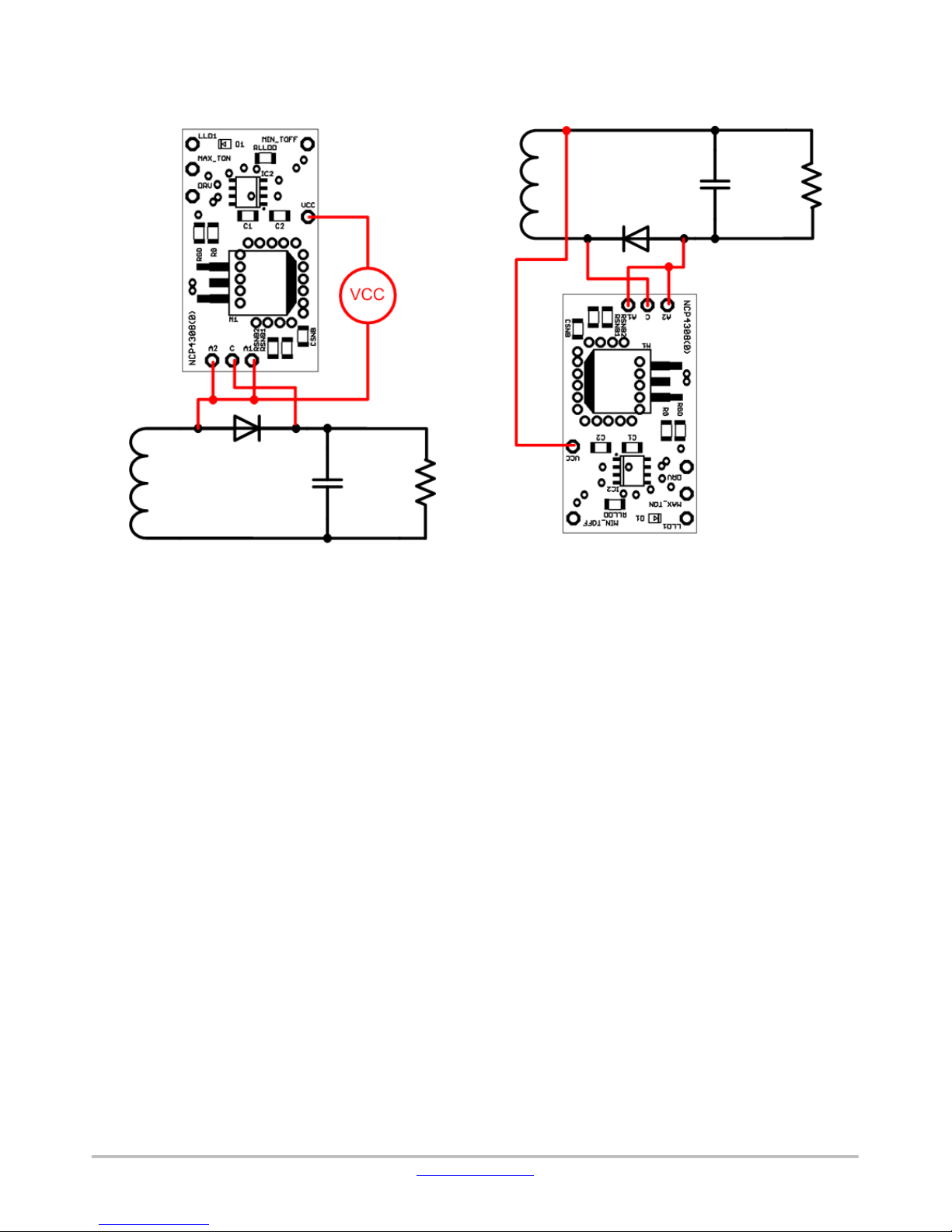
CONNECTION DIAGRAM
a) b)
Figure 2. Possible Connections into Circuit
The evaluation board can be connected in circuit where
the rectification diode is in the positive or negative branch.
When connection to a positive branch is used, it is necessary
to use an external power supply (or auxiliary winding with
rectification) to provide power to the evaluation board. VCC
should be referenced to A1 or A2 points.
www.onsemi.com
2
Page 3
EVBUM2520/D
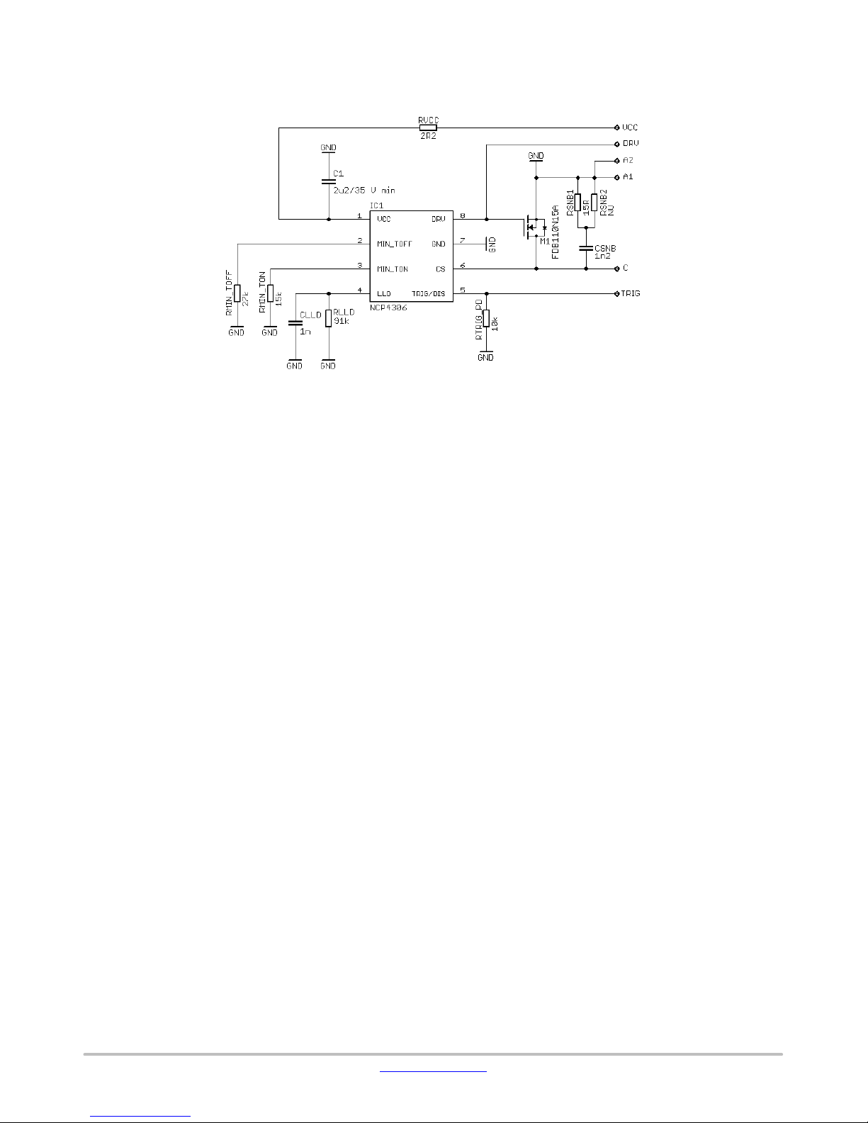
EVALUATION BOARD SCHEMATIC
Figure 3. Schematic of the NCP4306
The evaluation board was designed to support a minimal
external component count implementation. C1 is
decoupling capacitor that should be placed as close as
possible to the VCC and GND pins. Resistors RMIN_TON
and RMIN_TOFF are used to set the protection interval
when the synchronous MOSFET is turned on and off. It may
be needed to adjust them according to used SMPS. RLLD
sets light load detection time and CLLD is optional for LLD
voltage decoupling. Components CSNB, RSNB1 and
RSNB2 form a snubber circuit.
Transistor M1 is 150 V V
capable with R
DS
DSON
of
9.3 mW typ@10 V.
www.onsemi.com
3
Page 4

EVBUM2520/D
CIRCUIT LAYOUT
The PCB consists of a 2 layer FR4 board with 35 mm
copper cladding. All components are surface mount. Critical
component such as blocking capacitor C1 has to be placed
carefully near the IC. The synchronous driver path to the
MOSFET was done with very low resistance and parasitic
inductance to minimize emissions and minimize turn−on
Figure 4. Top Layer
and turn−off times. The same is true for the CS pin. For the
CS pin, a kelvin contact was done to be able to sense the
voltage directly at the drain. Improper connection of the
GND and CS connects can impact the turn−off process
especially when a very low R
MOSFET is used.
DSON
Figure 5. Bottom Layer
www.onsemi.com
4
Page 5

EVBUM2520/D
Figure 6. Top Side Components
Figure 7. Bottom Side Components
www.onsemi.com
5
Page 6

EVBUM2520/D
Figure 8. Evaluation Board Photos
www.onsemi.com
6
Page 7

EVBUM2520/D
BILL OF MATERIAL
Table 2. BILL OF MATERIAL FOR THE NCP4306 PUT−IN BOARD D2PAK 150 V
Designa-
tor
C1 1 Ceramic Capacitor
Qty Description Value Tolerance Footprint Manufacturer
2.2 mF / 50 V
10% 1206 KEMET C1206C225K5RACTU Yes
CLLD 1 Ceramic Capacitor 1n 20% 0805 KEMET C0805C102M5RACTU Yes
CSNB 1 Ceramic Capacitor 1n2 5% 1206 TDK
IC1 1 Secondary Side
M1 1 N−Channel Power
RVCC 1 Resistor SMD
RLLD 1 Resistor SMD
R
MIN_TOFF
R
MIN_TON
R
TRIG_PD
RSNB1 1 Resistor SMD
RSNB2 1 Resistor SMD NU − 1206 − − Yes
Synchronous
Rectification
Controller
MOSFET
1 Resistor SMD
1 Resistor SMD
1 Resistor SMD
NCP4306AAD
ZZZA
− SOIC−08 ON
FDB110N15A − D2PAK ON
2.2 W
91 kW
27 kW
15 kW
10 kW
15 W
1% 0805 YAGEO RC0805FR−072R2L Ye s
1% 0805 YAGEO RC0805FR−0791KL Ye s
1% 0805 YAGEO RC0805FR−0727KL Ye s
1% 0805 YAGEO RC0805FR−0715KL Ye s
1% 0805 YAGEO RC0805FR−0710KL Ye s
1% 1206 YAGEO RC1206FR−0715RL Ye s
Corporation
Semiconductor
Semiconductor
Manufacturer Part
Number
C3216C0G2J122J085
AA
NCP4306AADZZZAD
R2G
FDB110N15A Yes
Substitution
Allowed
Yes
No
NOTE: All components are Pb−Free.
ON Semiconductor and are trademarks of Semiconductor Components Industries, LLC dba ON Semiconductor or its subsidiaries in the United States and/or other countries.
ON Semiconductor owns the rights to a number of patents, trademarks, copyrights, trade secrets, and other intellectual property. A listing of ON Semiconductor’s product/patent
coverage may be accessed at www.onsemi.com/site/pdf/Patent−Marking.pdf
ON Semiconductor makes no warranty, representation or guarantee regarding the suitability of its products for any particular purpose, nor does ON Semiconductor assume any liability
arising out of the application or use of any product or circuit, and specifically disclaims any and all liability, including without limitation special, consequential or incidental damages.
Buyer is responsible for its products and applications using ON Semiconductor products, including compliance with all laws, regulations and safety requirements or standards,
regardless of any support or applications information provided by ON Semiconductor. “Typical” parameters which may be provided in ON Semiconductor data sheets and/or
specifications can and do vary in different applications and actual performance may vary over time. All operating parameters, including “Typicals” must be validated for each customer
application by customer’s technical experts. ON Semiconductor does not convey any license under its patent rights nor the rights of others. ON Semiconductor products are not
designed, intended, or authorized for use as a critical component in life support systems or any FDA Class 3 medical devices or medical devices with a same or similar classification
in a foreign jurisdiction or any devices intended for implantation in the human body. Should Buyer purchase or use ON Semiconductor products for any such unintended or unauthorized
application, Buyer shall indemnify and hold ON Semiconductor and its officers, employees, subsidiaries, affiliates, and distributors harmless against all claims, costs, damages, and
expenses, and reasonable attorney fees arising out of, directly or indirectly, any claim of personal injury or death associated with such unintended or unauthorized use, even if such
claim alleges that ON Semiconductor was negligent regarding the design or manufacture of the part. ON Semiconductor is an Equal Opportunity/Affirmative Action Employer. This
literature is subject to all applicable copyright laws and is not for resale in any manner.
. ON Semiconductor reserves the right to make changes without further notice to any products herein.
PUBLICATION ORDERING INFORMATION
LITERATURE FULFILLMENT:
Literature Distribution Center for ON Semiconductor
19521 E. 32nd Pkwy, Aurora, Colorado 80011 USA
Phone: 303−675−2175 or 800−344−3860 Toll Free USA/Canada
Fax: 303−675−2176 or 800−344−3867 Toll Free USA/Canada
Email: orderlit@onsemi.com
◊
N. American Technical Support: 800−282−9855 Toll Free
USA/Canada
Europe, Middle East and Africa Technical Support:
Phone: 421 33 790 2910
Japan Customer Focus Center
Phone: 81−3−5817−1050
www.onsemi.com
7
ON Semiconductor Website: www.onsemi.com
Order Literature: http://www.onsemi.com/orderlit
For additional information, please contact your local
Sales Representative
EVBUM2520/D
 Loading...