

Page 1
NCP4305DGEVB
NCP4305 Synchronous
Rectification Evaluation
Board User's Manual
Table 1. GENERAL PARAMETERS
Supply
SMPS Type
LLC 5−35 V 40 V
Description
This evaluation board user’s manual describes a high efficiency
synchronous rectification evaluation board that can easily replace
a secondary side rectification diode in an SMPS.
The NCP4305 is used as synchronous rectification controller.
The evaluation board has very few external components and illustrates
how small and effective such a design can be.
The NCP4305 features a very precise 0 mV turn-off comparator that
supports even very low current flowing through the MOSFET even
when very low R
Key Features
Voltage
synchronous MOSFET s is used.
DSON
Reverse
Voltage
Effective
Resistance
0.9 mW
• Precise Turn-off Comparator
• Wide Input Voltage Range
• High Operation Frequency
• Strong MOSFET Driver
• High Efficiency
• Adjustable Minimum On and Off Times
• Light Load Detection Feature
• Capable to Operate in Positive and Negative Branch
• Small size
www.onsemi.com
EVAL BOARD USER’S MANUAL
© Semiconductor Components Industries, LLC, 2016
January , 2016 − Rev. 1
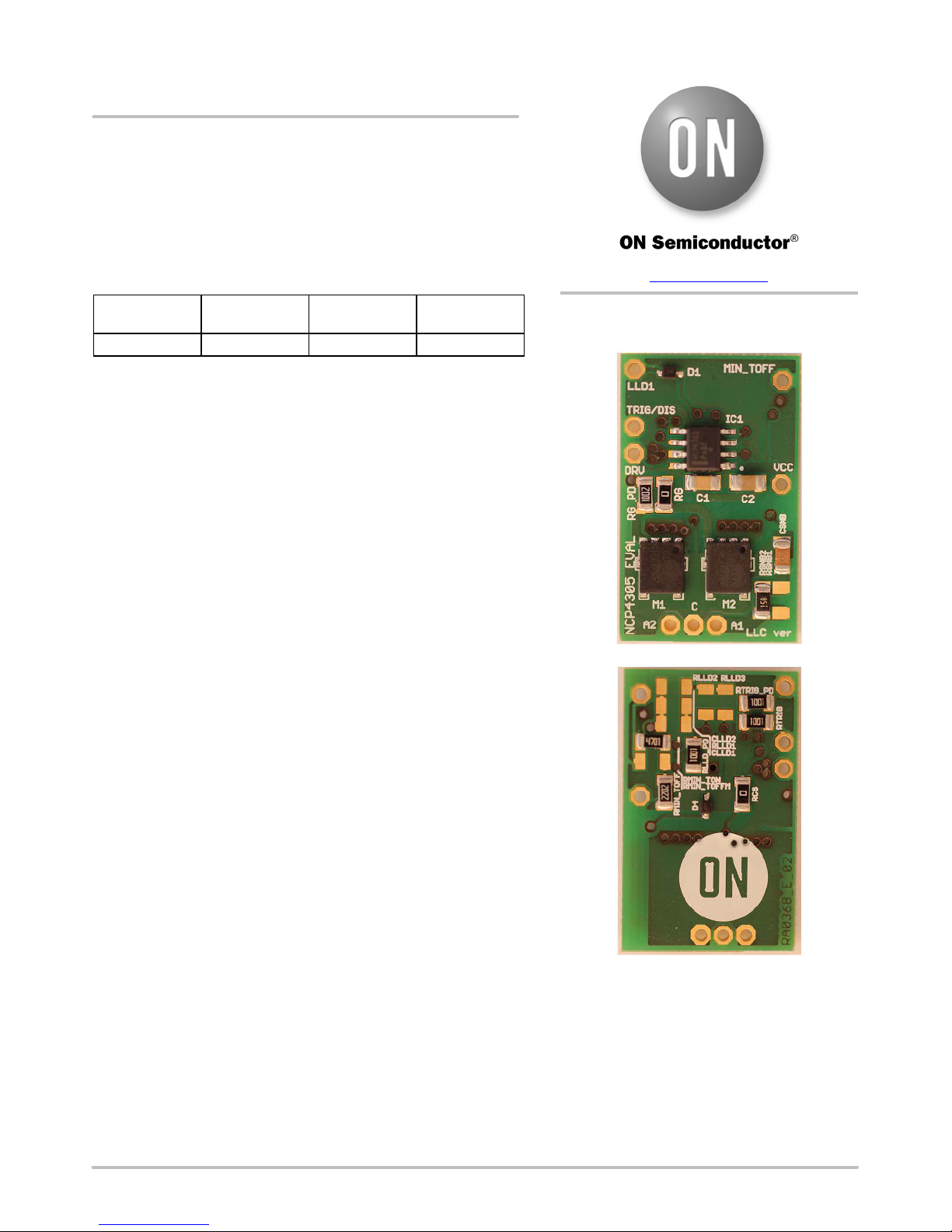
Figure 1. NCP4305 Evaluation Board
1 Publication Order Number:
EVBUM2350/D
Page 2
Connection Diagram
NCP4305DGEVB
VCC
+
+
VCC
A) B)
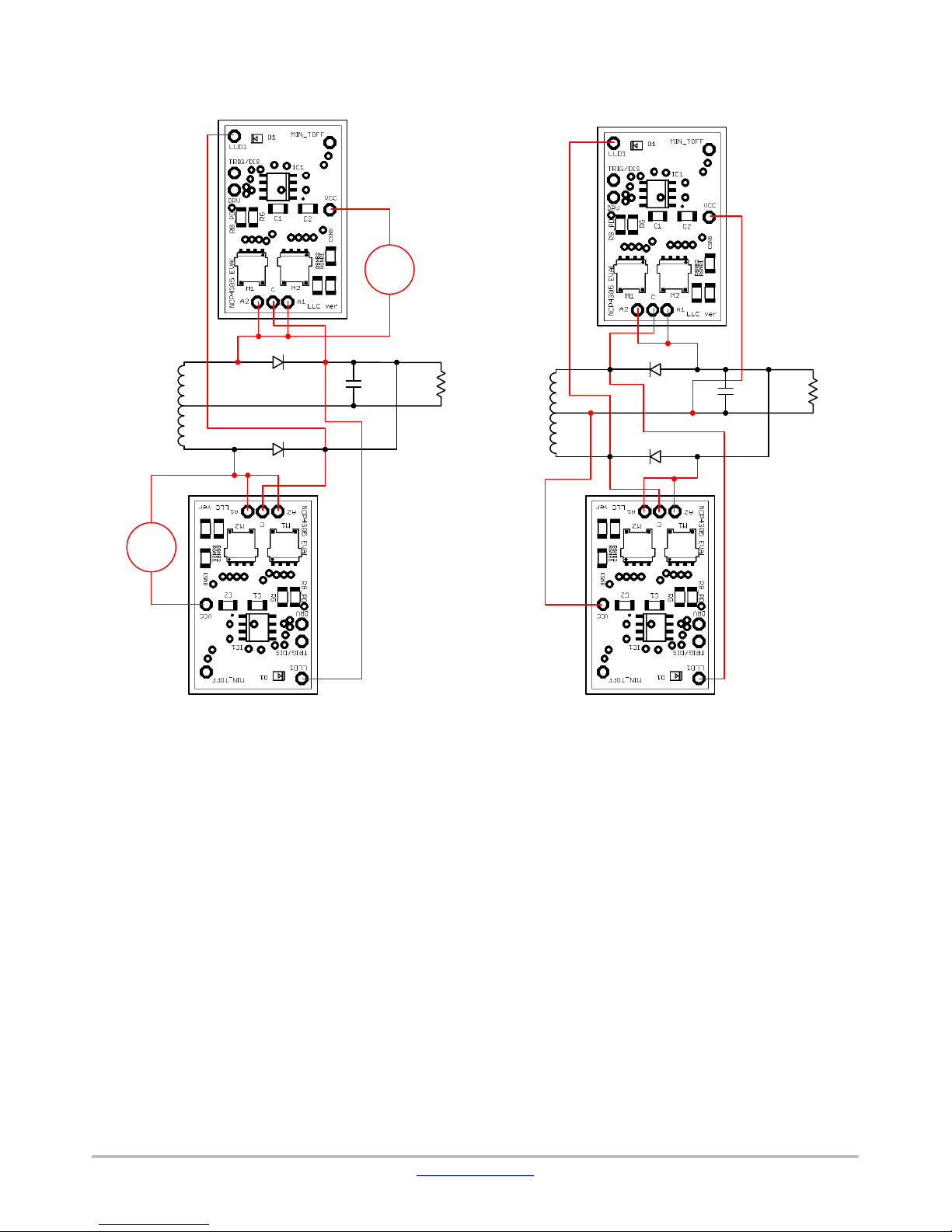
Figure 2. Possible Connections in to Circuit
The evaluation board can be connected in circuit where
the rectification diode is in the positive or negative branch.
When connection to a positive branch is used, it is necessary
to use an external power supply (or auxiliary winding with
rectification) to provide power to the evaluation board. VCC
should be referenced to A1 or A2 points. When LLD
function is used it is needed to connect LLD1 pin with
opposite side rectifier cathode.
www.onsemi.com
2
Page 3

Evaluation Board Schematic
MIN_TOFF
C1
100 nF
R
MIN_TOFFM
NU
22 kW
MIN_TON
R
LLD1
R
LLD2
NU
NU
4.7 kW
R
C
LLD1
NU
MIN_TOFF
R
GND GND
GNDGND
C
NU
R
R
LLD3
NU
LLD2
C2
1 mF/35 V
1
2
3
4
LLDD_PD
10 kW
LLD
NCP4305DGEVB
IC1
VCC
MIN_TOFF
MIN_TON
LLD
NCP4305S08
DRV
GND
CS
TRIG/DIS
GND
D4
BAS20
D1
BAS20
VCC
DRV
GND GND
G_PD
10 kW
R
R
G
TRIG_PD
R
GND
1 kW
GND
0 W
NVMFS5830
R
CS
0 W
M1
R
1 kW
M2
TRIG
8
7
6
5
SNB1
R
15 kW
C
SNB
3.9 nF
A2
A1
SNB2
NU
R
C
TRIG/DIS
LLD1
Figure 3. Schematic of the NCP4305
The evaluation board was designed to support a minimal
external component count implementation. C1 and C2 are
decoupling capacitors. They should be placed as close as
possible to the VCC and GND pins. Resistors R
R
MIN_TOFF
are used to set the protection interval when the
MIN_TON
and
synchronous MOSFET is turned on and off. Resistor
R
MIN_TOFFM
is placed there to support a situation when an
external circuit provides control for minimum off-time
modulation. This is needed only in situations when the
minimum off-time cannot be set across the whole range of
power supply operation. Resistor R
down for TRIG pin and R
A position for a gate resistor R
is only protection resistor.
TRIG
is provided in case there is
G
TRIG_PD
is only pull
a need to slow down the MOSFET switching process. The
turn-off (and also the turn-on) threshold can be lowed when
resistor R
is used. Components C
CS
SNB
, R
SNB1
and R
SNB2
form a snubber circuit.
LLD circuit consists of C
R
and D4. Purpose of circuit is to estimate output
LLD3
LLD1
, C
LLD2
, R
LLD1
, R
LLD2
power. This can be done in two ways. The first is to measure
duty cycle of skip burst. LLD circuit time constant is high
and it filters and averages duty cycle ratio. This is good for
systems which transfer low energy during skip each switch
cycle. When duty cycle of skip bursts is low NCP4305 enters
disable mode to save energy , when it is higher SR controller
starts to operate and SR transistor gate voltage is modulated
according to skip duty cycle. The second option is for system
which transfers lot of energy in few first pulses in skip and
then transferred energy is minimal. In this case LLD circuit
time constant is low and R
resistance is close to 0. LLD
LLD3
pin voltage drops down in first switching pulse in skip mode
and NCP4305 wakes up fast and allows using fully open SR
transistor. When skip burst ends, LLD voltage goes high and
if time between skip bursts is long enough NCP4305 enters
disable mode to save energy.
Circuit Layout
The PCB consists of a 2 layer FR4 board with 35 mm
copper cladding. All components are surface mount and
most of the components that may require adjustment are on
the same side and use 1206 values for easy rework. Critical
component such as blocking capacitors C1 and C2 have to
be placed carefully near the IC. The synchronous driver path
,
to the MOSFETs was done with very low resistance and
parasitic inductance to minimize emissions and minimize
turn-on and turn-off times. The same is true for the CS pin.
For the CS pin, a kelvin contact was done to be able to sense
the voltage directly at the drain. Improper connection of the
GND and CS connects can impact the turn-off process
especially when a very low R
MOSFET s are used.
DSON
www.onsemi.com
3
Page 4

NCP4305DGEVB
Figure 4. Top Layer
Figure 5. Bottom Layer
Figure 6. Top Side Components
www.onsemi.com
4
Page 5

NCP4305DGEVB
Figure 7. Bottom Side Components
Figure 8. Evaluation Board Photo − Top Side
Figure 9. Evaluation Board Photo − Bottom Side
www.onsemi.com
5
Page 6

NCP4305DGEVB
P
al
Table 2. BILL OF MATERIALS FOR NCP4305 PUT-IN BOARD SO-8FL (Note1)
Manufacturer
Parts Qty Description Value Tolerance Footprint Manufacturer
C1 1 Ceramic Capacitor 100 nF 10% 1206 Kemet C1206X104K5RACTU Yes
C2 1 Ceramic Capacitor
C
, C
LLD1
LLD2
C
SNB
D1, D4 2 Switching Diode BAS20HT1G − SOD−323 ON Semiconductor BAS20HT1G Yes
IC1 1 Secondary Side
M1, M2 2 N-Channel Power
RCS, R
R
G_PD
R
LLD_PD
R
TRIG
R
TRIG_PD
R
, R
LLD1
LLD2
R
LLD3
R
SNB2
R
MIN_TOFFML
R
MIN_TOFF
R
MIN_TON
R
SNB1
2 − NU − 1206 − − Yes
1 Ceramic Capacitor 3.9 nF − 1206 Kemet C1206C392K5RACTU Yes
Synchronous
Rectification Controller
MOSFET
2 Resistor SMD
G
1 Resistor SMD
,
3 Resistor SMD
,
,
5 Resistor SMD NU − 1206 − − Yes
,
,
1 Resistor SMD
1 Resistor SMD
1 Resistor SMD
1 mF/50V
NCP4305D − SOIC−08 ON Semiconductor NCP4305DDR2G No
NVMFS5830NL − SO−8FL ON Semiconductor NVMFS5830NLT1G Yes
0 W
10 kW
1kW
22 kW
4.7 kW
15 W
10% 1206 Kemet C1206X105K5RACTU Yes
5% 1206 Yageo RC1206JR−070RL Yes
1% 1206 Yageo RC1206FR−0710KL Yes
1% 1206 Yageo RC1206FR−071KL Yes
1% 1206 Yageo RC1206FR−0722KL Yes
1% 1206 Yageo RC1206FR−074K7L Yes
1% 1206 Yageo RC1206FR−0715RL Yes
1. All parts are Pb-Free
Part Number
Substitution
Allowed
ON Semiconductor and the are registered trademarks of Semiconductor Components Industries, LLC (SCILLC) or its subsidiaries in the United States and/or other countries.
SCILLC owns the rights to a number of patents, trademarks, copyrights, trade secrets, and other intellectual property. A listing of SCILLC’s product/patent coverage may be accessed
at www.onsemi.com/site/pdf/ Patent− Marking.pdf . S CILLC reserves t he right to m ake changes wit hout further notice to any products h erein. SCILLC makes no warranty, representation
or guarantee regarding the suitability of its products for any particular purpose, nor does SCILLC assume any liability arising out of the application or use of any product or circuit, and
specifically disclaims any and all liability, including without limitation special, consequential or incidental damages. “Typical” parameters which may be provided in SCILLC data sheets
and/or specifications can and do vary in different applications and actual performance may vary over time. All operating parameters, including “Typicals” must be validated for each
customer application by customer’s technical e xperts. SCILLC does not convey any license under i ts p atent rights nor the rights of others. S CILLC p roduct s a re n ot d esigned, i nt ended,
or authorized for use as components in systems intended for surgic al i mplant into the body, or other applications intended to support or sustain life, or for any other application in which
the failure of the SCILLC product could create a situation where personal injury or death may occur. Should Buyer purchase or use SCILLC products for any such unintended or
unauthorized application, Buyer shall indemnify and hold SCILLC and its officers, em ployees, subsidiaries, affiliates, and distributors harmless against all claims, costs, damages, and
expenses, and reasonable at torney f ees a r ising o ut o f, d irectly o r indirectly, any claim o f p ersonal i njury o r d eath a ssociated w ith s uch u nint ended o r u nauthorized u se, e ven if such claim
alleges that SCILLC was negligent r egarding the design o r manuf acture o f t he p art. SCILLC is an E qual O pportunity/Af firmat ive A ction E mployer . T his l iterature i s subject to all a pplicable
copyright laws and is not for resale in any manner.
UBLICATION ORDERING INFORMATION
LITERATURE FULFILLMENT:
Literature Distribution Center for ON Semiconductor
19521 E. 32nd Pkwy, Aurora, Colorado 80011 USA
Phone: 303−675−2175 or 800−344−3860 Toll Free USA/Canada
Fax: 303−675−2176 or 800−344−3867 Toll Free USA/Canada
Email: orderlit@onsemi.com
N. American Technical Support: 800−282−9855 Toll Free
USA/Canada
Europe, Middle East and Africa Technical Support:
Phone: 421 33 790 2910
Japan Customer Focus Center
Phone: 81−3−5817−1050
www.onsemi.com
6
ON Semiconductor Website: www.onsemi.com
Order Literature: http://www.onsemi.com/orderlit
For additional information, please contact your loc
Sales Representative
EVBUM2350/D
 Loading...