

Page 1

© Semiconductor Components Industries, LLC, 2011
July, 2011 − Rev. 2
1 Publication Order Number:
EVBUM2010/D
NCP2811AMTTXGEVB
NCP2811AMTTX Evaluation
Board User's Manual
Description
NCP2811 is a dual audio power amplifier designed for portable
communication device applications such as mobile phones. This board
showcases the A version of this part in the WQFN12 package. This
part is capable of delivering 27 mW of continuous average power into
a 16 W load from a 2.7 V power supply with a THD+N of 1%.
Based on the power supply delivered to the device, an internal
power management block generates a symmetrical positive and
negative voltage. Thus, the internal amplifiers provide outputs
referenced to Ground. In this True Ground configuration, the two
external heavy coupling capacitors can be removed. It offers
significant space and cost savings compared to a typical stereo
application.
Figure 1. NCP2811AMTTXGEVB Board Picture
http://onsemi.com
EVAL BOARD USER’S MANUAL
Page 2
NCP2811AMTTXGEVB
http://onsemi.com
2
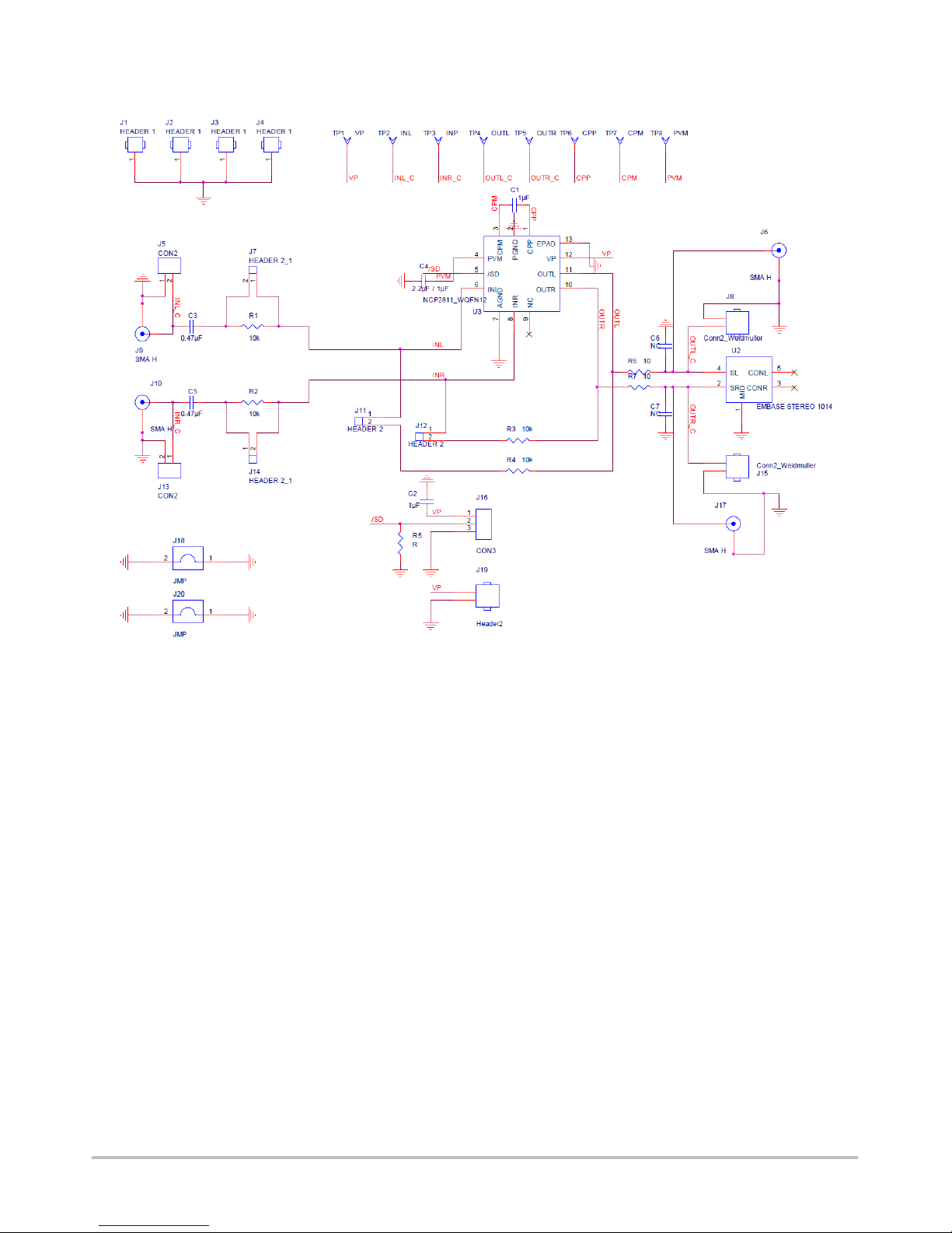
Figure 2. NCP2811AMTTXGEVB Board Schematic
Page 3

NCP2811AMTTXGEVB
http://onsemi.com
3
Figure 3. NCP2811AMTTXGEVB Board Layout (Top View)
Figure 4. NCP2811AMTTXGEVB Board Layout (Bottom View)
Page 4

NCP2811AMTTXGEVB
http://onsemi.com
4
Table 1. BILL OF MATERIALS
Item Part Description Ref. PCB
Footprint
Manufacturer Manufacturer Reference
1 NCP2811 Audio
Amplifier
ON Semiconductor NCP2811
2
SMD Resistor 10KW
R1, R2, R3, R4 0603 Panasonic ERJ−3GEY103V
3 Ceramic Capacitor
1 mF 6.3 V X5R
C1, C2, C3, C4, C5 0603 Murata GRM185R60J105KA01
4 Stereo Connector U2 CUI Inc. SJ1−3515N
5 Jumper Header
Vertical Mount, 2
positions, 100mils
J16 100 mils Tyco Electronics / AMP 5−826629−0
6 I/O Connector, 2
positions
J8, J19, J15 200 mils Phoenix Contact 1757242
7 Jumper Connector J18, J20 400 mils Harwin D3082−B01
8 Not Mounted R5, J9, J10, J6,
J17,C6, C7
9 Shorted R6, R7 0603
NCP2811A OR NCP2811B CONFIGURATION
V.1 NCP2811A
Connect J11, J12. Put 10kohms on R1, R2, R3, R4. Disconnect J7, J14.
V.1 NCP2811B
Connect J7, J14. Disconnect J11, J12, R1, R2, R3, R4.
NCP2811 TEST PROCEDURE
Output Power:
1. Set Vp = 3.6 V to power supply connector (J16).
2. Set an 16 W load (resistance) on the output connectors (J8 and J17).
3. With the function generator, set a single ended signal at 1 kHz and 0.5 Vrms input signal on the left and right inputs.
Apply this signal J5 and J13 connectors.
a. On the NCP2811A, as R1 = R2 = R3 = R4 = 10k, OUTL_C and OUTR_C will see 0.5 Vrms. Place an
oscilloscope probe on each output. You should get 0.5 Vrms output signal with a “perfect sine wave”. That is to
say no clipping at the minima and maxima of the sine wave.
b. On the NCP2811B, the gain is internally set to -1.5 V/V, OUTL_C and OUTR_C will see 0.75 Vrms. Place an
oscilloscope probe on each output. You should get 0.75 Vrms output signal with a “perfect sine wave”. That is
to say no clipping at the minima and maxima of the sine wave.
Quiescent Current:
Check the quiescent current. Place an 16 W load on each output (J8, J17); no input signal. Vp set to 3.6 V and J6 closed. You
should measure around 6 mA.
Page 5

NCP2811AMTTXGEVB
http://onsemi.com
5
ON Semiconductor and are registered trademarks of Semiconductor Components Industries, LLC (SCILLC). SCILLC reserves the right to make changes without further notice
to any products herein. SCILLC makes no warranty, representation or guarantee regarding the suitability of its products for any particular purpose, nor does SCILLC assume any liability
arising out of the application or use of any product or circuit, and specifically disclaims any and all liability, including without limitation special, consequential or incidental damages.
“Typical” parameters which may be provided in SCILLC data sheets and/or specifications can and do vary in different applications and actual performance may vary over time. All
operating parameters, including “Typicals” must be validated for each customer application by customer’s technical experts. SCILLC does not convey any license under its patent rights
nor the rights of others. SCILLC products are not designed, intended, or authorized for use as components in systems intended for surgical implant into the body, or other applications
intended to support or sustain life, or for any other application in which the failure of the SCILLC product could create a situation where personal injury or death may occur. Should
Buyer purchase or use SCILLC products for any such unintended or unauthorized application, Buyer shall indemnify and hold SCILLC and its officers, employees, subsidiaries, affiliates,
and distributors harmless against all claims, costs, damages, and expenses, and reasonable attorney fees arising out of, directly or indirectly, any claim of personal injury or death
associated with such unintended or unauthorized use, even if such claim alleges that SCILLC was negligent regarding the design or manufacture of the part. SCILLC is an Equal
Opportunity/Affirmative Action Employer. This literature is subject to all applicable copyright laws and is not for resale in any manner.
PUBLICATION ORDERING INFORMATION
N. American Technical Support: 800−282−9855 Toll Free
USA/Canada
Europe, Middle East and Africa Technical Support:
Phone: 421 33 790 2910
Japan Customer Focus Center
Phone: 81−3−5773−3850
EVBUM2010/D
LITERATURE FULFILLMENT:
Literature Distribution Center for ON Semiconductor
P.O. Box 5163, Denver, Colorado 80217 USA
Phone: 303−675−2175 or 800−344−3860 Toll Free USA/Canada
Fax: 303−675−2176 or 800−344−3867 Toll Free USA/Canada
Email: orderlit@onsemi.com
ON Semiconductor Website: www.onsemi.com
Order Literature: http://www.onsemi.com/orderlit
For additional information, please contact your local
Sales Representative
 Loading...