

Page 1
NCP1835B
Integrated Li−Ion Charger
NCP1835B is an integrated linear charger specifically designed to
charge 1−cell Li−Ion batteries with a constant current, constant
voltage (CCCV) profile.
Its low input voltage capability, adjustable charge current, ability
to maintain regulation without a battery, and its onboard thermal
foldback make it versatile enough to charge from a variety of wall
adapters. The NCP1835B can charge from a standard wall adapter or
from the USB port. It has been optimized to charge low capacity
batteries such as those found in wireless headsets and flash
memory−based MP3 players.
http://onsemi.com
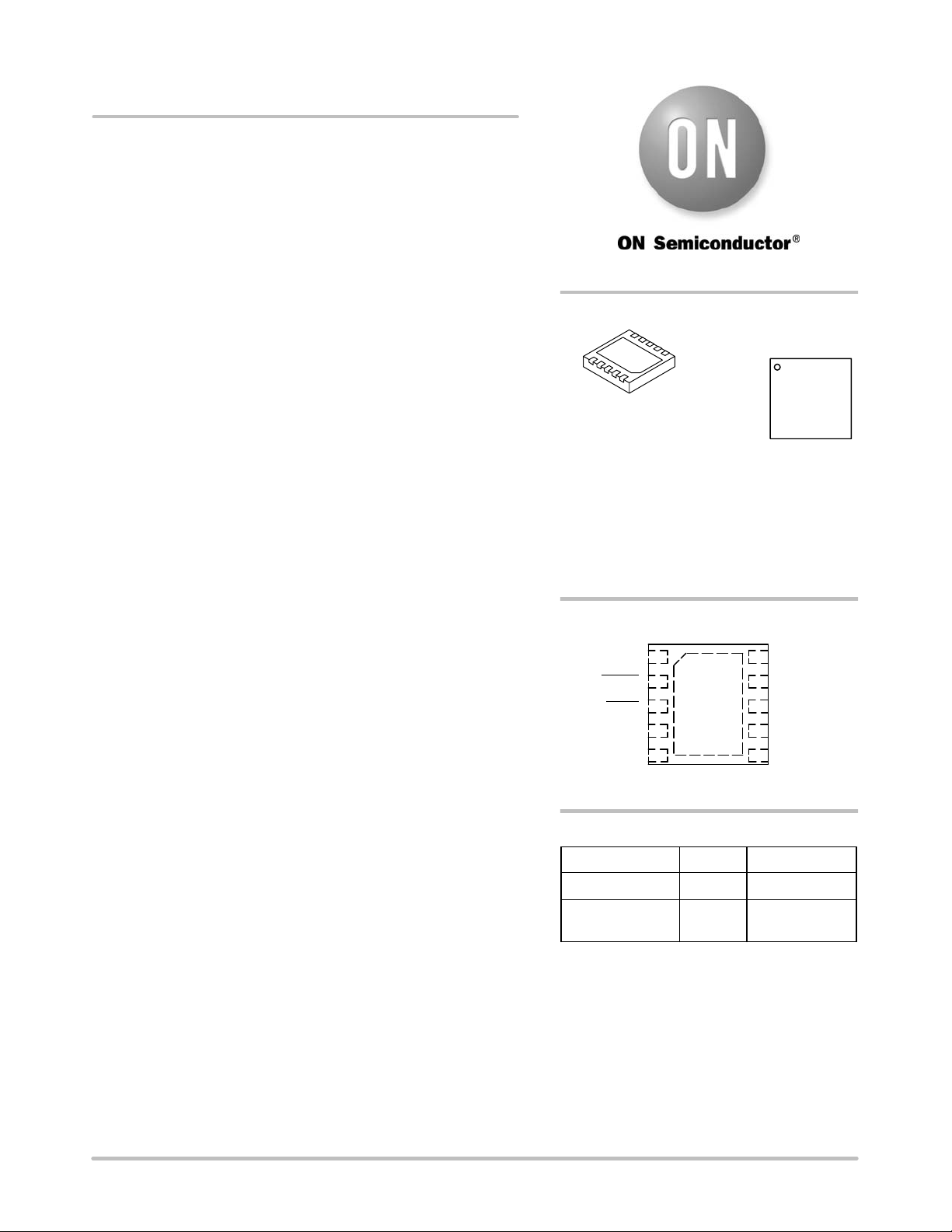
MARKING
DIAGRAM
Features
• Integrated Voltage and Current Regulation
• No External MOSFET, Sense Resistor or Blocking Diode Required
• Charge Current Thermal Foldback
• Integrated Pre−charge Current for Conditioning a Deeply
Discharged Battery
• Integrated End−of−Charge (EOC) Detection
• 1% Voltage Regulation
• 4.2 V Regulated Output Voltage
• Regulation Maintained without a Battery Present
• Programmable Full Charge Current
• Open−Drain Charger Status and Fault Alert Flags
• 2.8 V Output for AC Present Indication and Powering Charging
Subsystems
• Minimum Input Voltage of 2.4 V Allows Use of Current Limited
Adapters
• Automatically Recharging if Battery Voltage Drops after Charging
Cycle is Completed
• Low Profile 3x3 mm DFN Package
• Pb−Free Package is Available
T ypical Applications
• Wireless Headsets
• MP3 Players
• USB Appliances
• Battery Operated Devices
1
1835B
10
9
8
7
6
ALYWG
G
BAT
VSNS
ISEL
V2P8
EN
Shipping
†
1
DFN 3x3
MN SUFFIX
CASE 485C
1835B = Device Code
A = Assembly Location
L = Wafer Lot
Y = Year
W = Work Week
G = Pb−Free Package
(Note: Microdot may be in either location)
PIN CONNECTIONS
V
1
CC
FAULT
CFLG
TIMER
Device
NCP1835BMNR2 DFN−10 3000 Units/Reel
2
DFN 3x3
3
4
GND
5
(Top View)
ORDERING INFORMATION
Package
© Semiconductor Components Industries, LLC, 2006
September, 2006 − Rev . 4
NCP1835BMNR2G DFN−10
(Pb−Free)
†For information on tape and reel specifications,
including part orientation and tape sizes, please
refer to our Tape and Reel Packaging Specification
Brochure, BRD8011/D.
1 Publication Order Number:
3000 Units/Reel
NCP1835B/D
Page 2
NCP1835B
V
in
CFLG
EN
Microprocessor
V2P8
VSNS
NCP1835B
BAT
GND
15 nF
C
T
0.1 mF
C
2p8
4.7 mF
C
out
V
in
4.7 mF
FAULT
V
CC
C
in
ISEL TIMER
1.6 M
R
ISEL
GND
Figure 1. Typical 50 mA Application Circuit
PIN FUNCTION DESCRIPTION
Pin Symbol Description
1 V
CC
2 FAULT An open−drain output indicating fault status. This pin is pulled LOW under any fault conditions. A FAULT condition
3 CFLG An open−drain output indicating charging or end−of−charge states. The CFLG pin is pulled LOW when the charger
4 TIMER Connecting a timing capacitor, C
5 GND Ground pin of the IC. For thermal consideration, it is recommended to solder the exposed metal pad on the back-
6 EN Enable logic input. Connect the EN pin to LOW to disable the charger or leave it floating to enable the charger .
7 V2P8 2.8 V reference voltage output. This pin outputs a 2.8 V voltage source when an adapter is present. The maximum
8 ISEL The full charge current (I
9 VSNS Battery voltage sense pin. Connect this as close as possible to the battery input connection.
10 BAT Charge current output. A minimum 4.7 mF capacitor is needed for stability when the battery is not attached.
Input Supply Voltage. Provides power to the charger. This pin should be bypassed with at least a 4.7 mF ceramic
capacitor to ground.
resets the counter.
is charging a battery. It is forced open when the charge current drops to I
latched until a recharge cycle or a new charge cycle starts.
between this pin and ground to set end−of−charge timeout timer.
TIMEOUT = 14*C
Trickle Charge has a time limit of 1/8 of the TIMEOUT period.
/1.0 nF (minute). The total charge for CC and CV mode is limited to the length of TIMEOUT.
TIME
TIME
. This high impedance mode will be
EOC
side of the package to ground.
loading for this pin is 2.0 mA.
) can be set by connecting a resistor, R
For best accuracy, a resistor with 1% tolerance is recommended.
FCHG
, from the ISEL pin to ground.
ISEL
http://onsemi.com
2
Page 3
NCP1835B
V
CC
V2P8
CFLG
FAULT
Startup,
Control
& Clamp
V2P8
VCC
Resistor
Dividers
Bias Circuits
VREF
Chip
Enable
EN GNDTIMER
Figure 2. Detailed Block Diagram
Control
LOGIC
TIMER
Temp
CC
CV
VREF
Recharge
Comp
Precharge
Comp
Timer
Comp
IREF
Vbat
Resistor
Dividers
VREF
VREF
VREF
BAT
ISEL
VSNS
MAXIMUM RATINGS
Rating Symbol Value Unit
Supply Voltage V
Status Flag Output Pins V
Voltage Range for Other Pins V
Current Out from BAT Pin I
FAULT
CC
, V
O
CFLG
io
Thermal Characteristics
Thermal Resistance, Junction−to−Air (Note 3)
Power Dissipation, TA = 25°C (Note 3)
R
q
JA
P
D
Moisture Sensitivity (Note 4) MSL Level 1
Operating Ambient Temperature T
Storage Temperature T
A
stg
ESD
Human Body Model
Machine Model
HBM
MM
Stresses exceeding Maximum Ratings may damage the device. Maximum Ratings are stress ratings only. Functional operation above the
Recommended Operating Conditions is not implied. Extended exposure to stresses above the Recommended Operating Conditions may affect
device reliability.
1. This device series contains ESD protection and is tested per the following standards:
Human Body Model (HBM) per JEDEC standard: JESD22−A114.
Machine Model (MM) per JEDEC standard: JESD22−A115.
2. Latchup Current Maximum Rating: 150 mA per JEDEC standard: JESD78.
3. Measure on 1 inch sq. of 1 oz. copper area. R
sq. of 1 oz. copper area on 4 layer PCB that has 1 single signal layer with the additional 3 solid ground or power planes. The maximum package
is highly dependent on the PCB heatsink area. For example, R
q
JA
power dissipation limit must not be exceeded:
T
P
+
D
with R
q
4. Moisture Sensitivity Level per IPC/JEDEC standard: J−STD−020A.
JA
* T
J(max)
R
qJA
= 68.5°C/W, T
A
= 100°C, PD = 1.09 W.
J(max)
7.0 V
7.0 V
5.5 V
1.2 A
68.5
1.09
°C/W
W
−20 to 70 °C
−55 to 125 °C
2000
200
can be 38°C/W on 1 inch
q
JA
V
V
http://onsemi.com
3
Page 4
NCP1835B
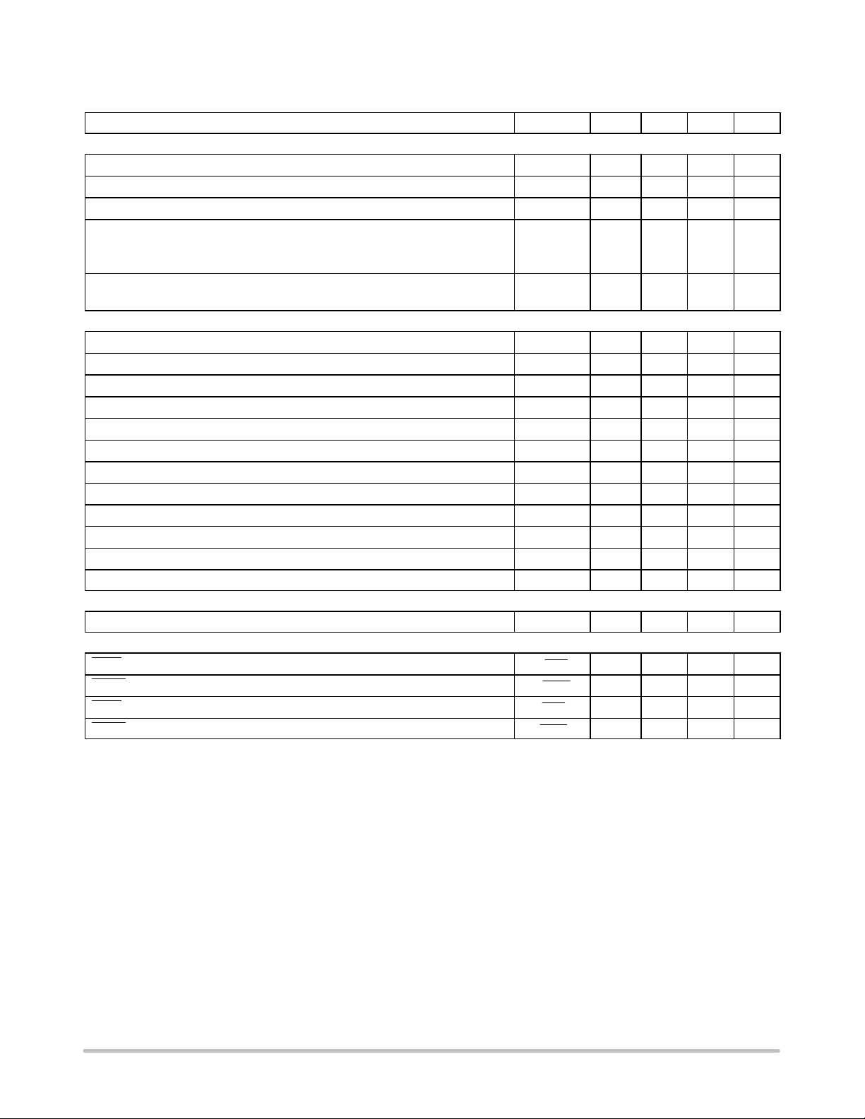
ELECTRICAL CHARACTERISTICS (Typical values are tested at V
= 5.0 V and room temperature, maximum and minimum values
CC
are guaranteed over 0°C to 70°C with a supply voltage in the range of 4.3 V to 6.5 V, unless otherwise noted.)
Characteristic Symbol Min Typ Max Unit
VCC SUPPL Y
Operating Supply Range V
Rising VCC Threshold V
Falling VCC Lockout Threshold V
CC
RISE
FALL
Quiescent VCC Pin Supply Current
Shutdown (EN = Low)
Normal Operation (EN = High)
Battery Drain Current
Manual Shutdown (VCC = 5.0 V , VSNS = 4.0 V, EN = Low)
I
VCC
I
VCC
I
BMS
CHARGING PERFORMANCE
Regulated Output Voltage in Constant Voltage (CV) Mode, I
Dropout Voltage (V
= 3.7 V , I
BAT
= 0.1 A) − − 80 120 mV
CHG
Pre−Charge Threshold Voltage V
Pre−Charge Current (R
Pre−Charge Current (R
= 2.7 MW, V
ISEL
= 270 kW, V
ISEL
= 2.0 V) I
BAT
= 2.0 V) I
BAT
Recommended Full Charge Current I
Full−Charge Current in Constant Current (CC) Mode (R
Full−Charge Current in Constant Current (CC) Mode (R
End−of−Charge Threshold (R
End−of−Charge Threshold (R
= 2.7 MW, V
ISEL
= 270 kW, V
ISEL
BAT
BAT
= V
= V
REG
REG
Recharge Voltage Threshold V
Thermal Foldback Limit (Junction Temperature) (Note 5) T
= 10 mA V
CHG
= 2.7 MW, V
ISEL
= 270 kW, V
ISEL
= 3.7 V) I
BAT
= 3.7 V) I
BAT
) I
) I
REG
PC
PC
PC
FCHG
FCHG
FCHG
EOC
EOC
RECH
LIM
4.158 4.200 4.242 V
OSCILLATOR
Oscillation Period (C
= 15 nF) T
TIME
OSC
STATUS FLAGS
CFLG Pin Recommended Maximum Operating V oltage V
FAULT Pin Recommended Maximum Operating Voltage V
CFLG Pin Sink Current (V
FAULT Pin Sink Current (V
= 0.8 V) I
CFLG
= 0.8 V) I
FAULT
CFLG
FAULT
CFLG
FAULT
5. Guaranteed by design. Not tested in production.
2.8 − 6.5 V
3.0 3.4 3.95 V
2.0 2.4 2.8 V
−
−
30
600
−
−
mA
mA
− − 3.0 mA
2.52 2.8 3.08 V
1.0 20 30 mA
30 50 65 mA
30 − 300 mA
30 45 58 mA
280 310 360 mA
1.0 4.0 11 mA
26 34 42 mA
3.80 4.03 4.155 V
− 100 − °C
2.4 3.0 3.6 ms
− − 6.5 V
− − 6.5 V
5.0 − − mA
5.0 − − mA
http://onsemi.com
4
Page 5
NCP1835B
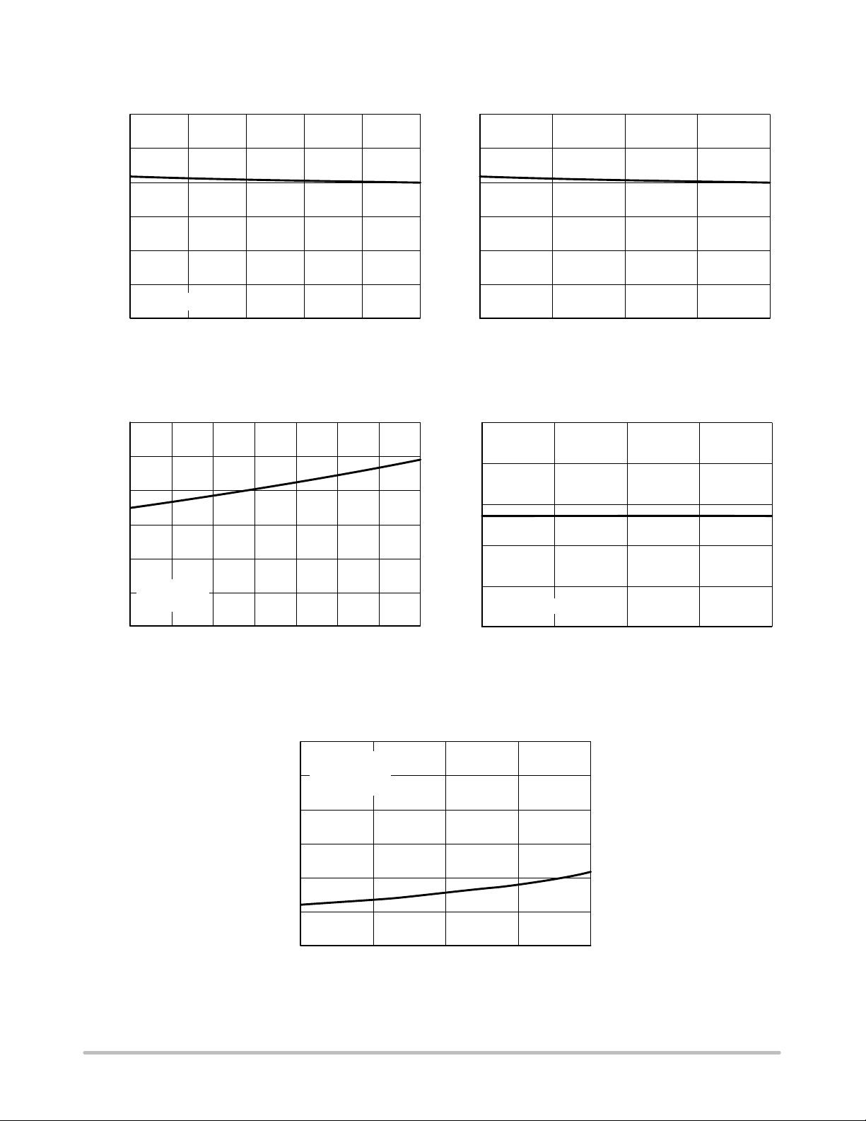
TYPICAL OPERATING CHARACTERISTICS
4.30
4.25
4.20
4.15
4.10
4.05
, REGULATED OUTPUT VOLTAGE (V)
REG
V
VCC = 5 V
4.00
0 0.06 0.12 0.18 0.24 0.3
I
, CHARGE CURRENT (A)
CHG
Figure 3. Regulated Output Voltage vs. Charge
Current
4.30
4.25
4.20
4.15
4.10
VCC = 5 V
4.05
V
floating
, REGULATED OUTPUT VOLTAGE (V)
REG
V
BAT
4.00
−50 −25 0 25 50 75
TA, AMBIENT TEMPERATURE (°C)
100 125
4.30
4.25
4.20
4.15
4.10
4.05
, REGULATED OUTPUT VOLTAGE (V)
4.00
REG
4.5 5 5.5 6 6.5
V
VCC, INPUT VOLTAGE (V)
Figure 4. Regulated Output Voltage (floating) vs.
Input Voltage
0.80
0.78
0.76
0.74
, ISEL VOLTAGE (V)
ISEL
V
0.72
V
= 3.7 V
BAT
0.70
4.5 5.0 5.5 6.0 6.5
VCC, INPUT VOLTAGE (V)
Figure 5. Regulated Output Voltage vs.
Temperature
3.00
V
floating
BAT
R
= 270 k
2.95
ISEL
I
V2P8
= 0
2.90
2.85
2.80
, V2P8 VOLTAGE (V)
2P8
V
2.75
2.70
4.5 5.0 5.5 6.0 6.5
VCC, INPUT VOLTAGE (V)
Figure 7. V2P8 Voltage vs. Input Voltage
http://onsemi.com
Figure 6. ISEL Voltage vs. Input Voltage
5
Page 6
5
V
, V2P8 VOLTAGE (V)
3.0
2.5
5
50
I
, TRICKLE CHARGE CURRENT (mA)
5
V
, RECHARGE VOLTAGE (V)
NCP1835B
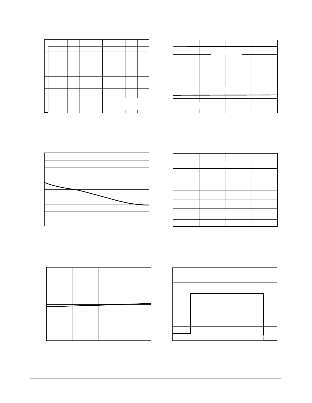
TYPICAL OPERATING CHARACTERISTICS
40
R
ISEL
= 270 kW
2.0
1.5
1.0
2P8
0.5
0.0
4.3 4.5 4.7 4.9 5.1
VCC, INPUT VOLTAGE (V)
Figure 8. V2P8 Voltage vs. Input Voltage Figure 9. Trickle Charge Current vs. Input Voltage
100
90
80
70
60
50
40
30
20
V
= 3.7 V
BAT
10
R
=270 kW
PC
ISEL
0
−50 −25 0 25 50 75
TA, AMBIENT TEMPERATURE (°C)
V
R
BAT
ISEL
= 3.7 V
= 270 kW
5.3 5.53.7 3.9 4.1
100 125
30
20
R
= 2.7 MW
ISEL
10
V
= 2.0 V
, TRICKLE CHARGE CURRENT (mA)
PC
I
BAT
0
4.5 5.0 5.5 6.0 6.
VCC, INPUT VOLTAGE (V)
400
350
R
ISEL
= 270 kW
V
300
250
200
150
100
R
, FULL CHARGE CURRENT (mA)
50
FCHG
I
0
ISEL
= 2.7 MW
4.5 5.0 5.5 6.0 6.
VCC, INPUT VOLTAGE (V)
BAT
= 3.7 V
Figure 10. Trickle Charge Current vs. Temperature Figure 11. Full Charge Current vs. Input Voltage
4.10
4.05
4.00
3.95
RECH
3.90
4.5 5.0 5.5 6.0 6.5
Figure 12. Recharge Voltage vs. Input Voltage
R
VCC, INPUT VOLTAGE (V)
= 270 kW
ISEL
http://onsemi.com
500
400
300
200
, CHARGE CURRENT (mA)
100
CHG
I
0
2.5 3.0 3.5 4.0 4.
Figure 13. Charge Current vs. Battery Voltage
6
VCC = 5 V
V
, BATTERY VOLTAGE (V)
BAT
Page 7

NCP1835B
DETAILED OPERATING DESCRIPTION
Overview
Rechargeable Li−Ion/Polymer batteries are normally
charged with a constant current (CC) until the terminal
voltage reaches a fixed voltage threshold, at which point a
constant voltage (CV) is applied and the current drawn by
the battery decays. The charging rate is determined by the
specific rating of the battery. For example, if the battery is
rated at 800 mA−hours, then the recommended maximum
charge rate is 800 mA. For a severely discharged cell, it
takes approximately 2.5−3.5 hours to recharge the battery
at the maximum rate. So, when one charges at less than the
maximum charge rate, the recharge time increases. Also,
the battery should not be continuously charged or the
battery could age faster than necessary. Because of this,
Li−Ion charging systems need to stop charging within a
prescribed time limit regardless of the charge rate.
The NCP1835B is a fully integrated, stand−alone 1−cell
Li−Ion charger which performs the primary battery
charging functions and includes a timer which will
terminate charging if the battery has not completed
charging within a prescribed time period. The charging rate
is user programmable up to 1.0 A and the end−of−charge
timer is also programmable. The NCP1835B has a thermal
foldback loop which reduces the charge rate if the junction
temperature is exceeded. The device also includes several
outputs which can be used to drive LED indicators or
interface to a microprocessor to provide status information.
The adapter providing power to the charger can be a
standard fixed output voltage such as a 5.0 V wall adapter
or it can be a simple current limited adapter.
The NCP1835B comes in two versions with output
voltage regulation thresholds of 4.2 or 4.242 V depending
on the requirements of the specific battery pack being used.
The user determines the charge current by selecting the
resistor R
and determines the length of the
ISEL
end−of−charge timeout timer by selecting the capacitor,
C
.
TIME
Charging Operation
Figure 13 outlines the charging algorithm of the
NCP1835B and Figure 14 graphically illustrates this.
When the charger is powered up and the input voltage rises
above the power−on, rising threshold (nominally 3.4 V),
the charger initiates the charging cycle.
The NCP1835B first determines the cell voltage. If it is
less than the pre−charge threshold (2.8 V), the IC
recognizes the battery as severely discharged. In this state,
the NCP1835B pre−conditions (trickle charges) the battery
by charging it at 10% of the full charge rate (IPC). This slow
charge prevents the battery from being damaged from high
fast charge currents when it is in a deeply discharged state.
The battery voltage should be trickle charged up to 2.8 V
before 1/8 of the preset end−of−charge time is expired. If
it cannot reach this voltage, than the battery is possibly
shorted or damaged. Therefore, the NCP1835B stops
charging and the pre−charge timeout signal asserts the
FAULT flag.
Once the cell voltage crosses the pre−charge threshold,
the device will transition to normal (full−rate) charging at
100% of the programmed full rate charge current (I
FCHG
As the NCP1835B charges the battery, the cell voltage rises
until it reaches the V
threshold, (4.2 or 4.242 V). At the
REG
maximum charge rate, it normally takes about 1 hour to
reach this point from a fully discharged state, and the
battery will be approximately 70−80% recharged. At this
point, the charge transitions to constant voltage mode
where the IC forces the battery to remain at a constant
voltage, V
current required to maintain V
. During this constant voltage state, the
REG
steadily decreases as the
REG
battery approaches full charge. Charge current eventually
falls to a very low value as the battery approaches a fully
charged condition.
The NCP1835B monitors the current into the battery
until it drops to 10% of the full charge rate. This is the
End−of−Charge (EOC) threshold. Normally it takes
1.5−2.5 hours to reach this point. Once the NCP1835B
reaches end−of−charge it opens the CFLG pin and enters
the EOC state. The IC continues to charge the battery until
it reaches TIMEOUT. At that point, the NCP1835B stops
charging. If the system does not reach EOC during the
TIMEOUT period, the NCP1835B views this as a system
fault and asserts the FAULT flag. If the battery voltage
drops below the recharge threshold (which can occur if the
battery is loaded), the IC reinitializes the charging
sequence and begins a new charge cycle. The recharge
voltage threshold, V
, is nominally 4.03 V.
RECH
In the inhibit state, the NCP1835B continues to monitor
the battery voltage, but does not charge the battery. Again,
if the battery voltage drops below the recharge threshold
the IC reinitializes the charging sequence and begins a new
charge cycle.
).
http://onsemi.com
7
Page 8

NCP1835B
Power Up
VCC > V
POR
Y
POR
Initialization
Reset Counter
Trickle
Charge
Charging Flow Chart
?
N
CC
Charge
CV
Charge
N
Trickle
Charge
Set FAULT Low
Latch Up Charger
V
> VPC?
SNS
N
1/8 TIMEOUT?
Y
EN Toggled?
V
≥ V
SNS
REG
?
Y
Ich < I
EOC
?
Y
Y
N
N
N
N
Constant
Current
Charge
TIMEOUT?
Y
Constant
Voltage
Charge
TIMEOUT?
Y
EOC Indication;
Set CFLG High
Keep FAULT High
Charger Inhibited
Reset Counter
Y
V
< V
SNS
N
TIMEOUT?
RECH
N
?
V
V
RECH
SNS
<
?
N
Y
Y
End−of−Charge
or F AULT
Y
N
Start Recharge
Inhibit
Figure 14. Charging Flow Chart
http://onsemi.com
8
Page 9

NCP1835B
V
BAT
I
charge
Trickle
ChargeCCChargeCVCharge
V
in
V
RISE
End of
Charge Recharging
Inhibit
Time
V
V
REG
REG
V
RECH
V
PC
V
REG
Time
I
CHG
I
CHG
I
PC
I
EOC
Time
CFLG
Time
FAULT
Time
V2P8
2.8 V
Time
0
Figure 15. Typical Charging Diagram
T able 1. Charge Status
Condition CFLG FAULT
Trickle, Constant Current and Constant V oltage Charge Low High
End−of−Charge or Shutdown Mode High High
Timeout Fault, V
< 0.35 V or V
ISEL
> 1.4 V High Low
ISEL
http://onsemi.com
9
Page 10

NCP1835B
Charge Status Indicator (CFLG)
CFLG is an open−drain output that indicates battery
charging or End−of−Charge (EOC) status. It is pulled low
when charging in constant current mode and constant
voltage mode. It will be forced to a high impedance state
when the charge current drops to I
. When the charger
EOC
is in shutdown mode, CFLG will also stay in the high
impedance state.
Fault Indicator (FAULT)
FAULT is an open−drain output that indicates that a
charge fault has occurred. It has two states: low or high
impedance. In a normal charge cycle, it stays in a high
impedance state. At fault conditions, it will be pulled low
and terminate the charge cycle. A timeout fault occurs
when the full charge or pre−charge timeouts are violated,
or if the voltage on ISEL is greater than 1.4 V or lower than
0.35 V. There are two ways to get the charger out of a fault
condition and back to a normal charge cycle. One can either
toggle the EN pin from GND to a floating state or reset the
input power supply.
Adapter Present Indicator (V2P8)
V2P8 is an input power supply presence indicator. When
the input voltage, VCC, is above the power on threshold
(V
, nominally 3.4 V) and is also 100 mV above the
RISE
battery voltage, it provides a 2.8 V reference voltage that
can source up to 2.0 mA. This voltage can also be used to
power a microprocessor I/O.
Enable/Disable (EN)
Pulling the EN pin to GND disables the NCP1835B. In
shutdown mode, the internal reference, oscillator, and
control circuits are all turned off. This reduces the battery
drain current to less than 3.0 mA and the input supply
current to 30 mA. Floating the EN pin enables the charger.
Thermal Foldback
An internal thermal foldback loop reduces the
programmed charge current proportionally if the die
temperature rises above the preset thermal limit (nominally
100°C). This feature provides the charger protection from
over heating or thermal damage. Figure 16 shows the full
charge current reduction due to die temperature increase
across the thermal foldback limit. For a charger with a
1.0 A constant charge current, the charge current starts
decreasing when the die temperature hits 100°C and is
reduced to zero when the die temperature rises to 110°C.
I
FCHG
X−100 mA/C
, CHARGE CURRENT
CHG
I
100°C
TJ, JUNCTION TEMPERATURE
Figure 16. Full Charge Current vs. Junction
Temperature
http://onsemi.com
10
Page 11

NCP1835B
0
70
I
(mA)
0
I
(mA)
600
APPLICATION INFORMATION
Input and Output Capacitor Selection
A 4.7 mF or higher value ceramic capacitor is
recommended for the input bypass capacitor. For the output
capacitor, when there is no battery inserted and the
NCP1835B is used as an LDO with 4.2 V or 4.242 V output
voltage, a 4.7 mF or higher value tantalum capacitor is
recommended for stability. With the battery attached, the
output capacitor can be any type with the value higher than
0.1 mF.
R
Resistor Selection for Programming Charge
ISEL
Current
A single resistor, R
between the ISEL pin and
ISEL,
ground, programs the pre−charge current, full−charge
current, and end−of−charge detection threshold. The
nominal voltage of ISEL is 0.8 V.
60
50
40
PC
30
20
10
C
Selection for Programming Charge Time
TIME
The NCP1835B offers an end−of−charge timeout timer
to prevent the battery from continuously charging which
can cause premature aging or safety issues. The timing
capacitor between TIMER pin and ground, C
TIME
, sets the
end−of−charge time, TIMEOUT, and the pre−charge
timeout. This capacitor is required for proper device
operation.
The internal oscillator charges C
to 1.2 V and then
TIME
discharges it to 0.6 V with 6 mA current in one period.
Therefore, the period of the oscillator is:
T
OSC
+ 2
TIME
c
I
C
+ 0.2 106 C
TIME
(sec)
(eq. 1)
C
dV
A 22−binary counter counts every oscillator period until
it reaches the maximum number corresponding to
end−of−charge time, TIMEOUT.
C
TIMEOUT + 222 T
OSC
+ 14
TIME
1nF
(minute)
(eq. 2)
The NCP1835B will terminate charging and give a
timeout signal if the battery has not completed charging
within the TIMEOUT period. The timeout signal then
forces the FAULT pin low.
The following Table 2 shows the desired TIMEOUT vs.
C
sizes. The C
TIME
is required for proper device
TIME
operation.
0
R
(kW)
ISEL
Figure 17. NCP1835 Pre−charge Current
500
400
300
FC
200
100
0
R
(kW)
ISEL
Figure 18. NCP1835 Full Charge Current
200
180016001400120010008006004002000
Table 2. TIMEOUT vs. C
C
(nF) TIMEOUT (minute)
TIME
0.47 6.6
1 14
5.6 78
8.2 115
10 140
15 210
33 462
56 784
TIME
Size
Thermal Considerations
The NCP1835B is housed in a thermally enhanced
3x3 mm DFN package. In order to deliver the maximum
power dissipation under all conditions, it is very important
that the user solders exposed metal pad under the package
160
1400120010008006004002000
to the ground copper area and then connect this area to a
ground plane through thermal vias. This can greatly reduce
the thermal impedance of the device and further enhance
its power dissipation capability and thus its output current
capability.
http://onsemi.com
11
Page 12

NCP1835B
I
Trickle
CV
Charging with Constant Voltage Adapters or Current
Limited Adapters
The NCP1835B can be powered from two types of
regulated adapters: a traditional constant voltage type or a
current limited type. Figure 19 illustrates the operation of
the linear charger powered with a standard constant voltage
adapter. The power dissipation in the linear charger is:
P
+ (VCC* V
dis
BAT)
I
CHG
(eq. 3)
The maximum power dissipation P1 happens at the
beginning of a full current charge, since this is the point that
the power supply and the battery voltage have the largest
difference. As the battery voltage rises during charging, the
power dissipation drops. After entering the constant
voltage mode, the power dissipation drops further due to
the decreasing charge current. The maximum power that
the linear charger can dissipate is dependent on the thermal
resistance of the device. In case the device can not handle
the maximum power P1, the thermal foldback loop reduces
Trickle
ChargeCCCharge
V
in
V
BAT
charge
V
PC
I
FCHG
CV
Charge Inhibit
V
REG
Time
Time
the charge current which limits the power dissipation to the
sustained level P2. Figure 19 shows this.
Using the adapter’s current limit can provide better
thermal performance than the above example. A current
limited adapter operates as a constant voltage adapter
before the charge current reaches the current limit. I
must be less than the programmed full charge current
I
. Once the current limit is reached, the adapter will
FCHG
source the current limit I
while its output voltage will
LIM
drop to follow the battery voltage. If the application uses
the adapter to power its systems while the battery is being
charged, this drooping voltage can be an issue.
The worst case power dissipation with a current limited
adapter occurs at the beginning of the constant voltage
mode, which is shown at point P3 in Figure 20. If P3 is
higher than P2, the maximum power dissipation that the
charger can handle, then the thermal foldback function will
be activated.
V
I
charge
V
BAT
in
ChargeCCCharge
V
PC
I
FCHG
I
LIM
Charge
V
REG
Inhibit
Time
Time
LIM
I
I
PC
P
dis
P1
P2
0
Figure 19. Typical Charge Curves with a Constant
Voltage Adapter
PCB Layout Recommendations
The recommended footprint for the 3x3 mm DFN
Time
Time
PC
P
dis
P3
0
Figure 20. Typical Charge Curves with a Current
Limited Adapter
Time
Time
package is included on the Package Dimension page. It is
critical that the exposed metal pad is properly soldered to
the ground copper area and then connected to a ground
plane through thermal vias. The maximum recommended
thermal via diameter is 12 mils (0.305 mm). Limited by the
size of the pad, six thermal vias should allow for proper
thermal regulation without sacrificing too much copper
area within the pad. The copper pad is the primary heatsink
and should be connected to as much top layer metal as
GND
possible to minimize the thermal impedance. Figure 21
illustrates graphically the recommended connection for the
Figure 21. Recommended Footprint
exposed pad with vias.
http://onsemi.com
12
Page 13

NCP1835B
V
The following is a NCP1835B Demo Board Schematic and suggested Bill of Materials.
NCP1835B
V
CC
(T8)
GND
(T9)
C5
FAULT
(T5)
R4
D1
CFLG
(T6)
R5
D2
TIMER
(T10)
C4
VCC
FAULT
CFLG
TIMER V2P8
GND
VCC
BAT
VSNS
ISEL
EN
R3
V2P8
(T4)
D3
C3
2
JP2
1
R8
R2
R9
R1
C1
2
JP1
1
+
−
C2
Figure 22. Demo Board Schematic
Table 3. Bill of Materials
Item Qty. Part Description Designators Suppliers Part Number
1 1 NCP1835B Integrated Li−Ion Charger (DFN−10) U1 ON Semiconductor NCP1835B
2 1 Chip Resistor "1% 0 W (0603) R1 Vishay CRCW06030R00F
3 2 Chip Resistor "1% 2.67 MW (0603) R2 Vishay CRCW06032674
4 1 Chip Resistor "1% 100 kW (0603) R3 Vishay CRCW06031003F
5 2 Chip Resistor "1% 1.0 kW (0603) R4, R5 Vishay CRCW06031001F
6 1 Chip Resistor "1% 432 W (0603) R8 Vishay CRCW06034320F
7 1 Chip Resistor "1% 274 kW (0603) R9 Vishay CRCW06032743F
8 1 Chip Capacitor 1.0 mF/16 V, "20% (0805) C1 Panasonic ECJGVB1C105M
9 1 Chip Capacitor 4.7 mF/10 V, "20% (3528−21) C2 Kemet T491A475K016AS
10 1 Chip Capacitor 0.1 mF/10 V, "10% (0402) C3 Panasonic ECJ0EB1A104K
11 1 Chip Capacitor 15 nF/16 V, "10% (0402) C4 Panasonic ECJ0EB1C153K
12 1 Chip Capacitor 4.7 mF/25 V, "20% (0805) C5 Panasonic ECJ2FB1E475M
13 1 SMT Chip LED Red D1 Agilent HSMH−C150
14 1 SMT Chip LED Green D2 Agilent HSMG−C150
15 1 SMT Chip LED Yellow D4 Agilent HSMY−C150
16 5 Test Pin T1, T2, T7,
T8, T9, T10
17 2 Header Pin Pinch = 2.54 mm JP1, JP2 AMP/Tyco 4−103747−0
AMP/Tyco 4−103747−0
BAT
(T1)
VSNS
(T7)
Li−Ion
Battery
GND
(T2)
http://onsemi.com
13
Page 14

MECHANICAL CASE OUTLINE
PACKAGE DIMENSIONS
SCALE 2:1
DFN10, 3x3, 0.5P
CASE 485C
ISSUE E
DATE 11 FEB 2016
2X
2X
10X
PIN ONE
REFERENCE
0.15 C
0.15
0.10 C
0.08 C
DETAIL A
K
PACKAGE
OUTLINE
D
A
B
E
C
TOP VIEW
D2
(A3)
A1
10X
DETAIL B
SIDE VIEW
15
E2
10 6
e
10X
b
BOTTOM VIEW
SOLDERING FOOTPRINT*
2.64
L1
ALTERNATE TERMINAL
A1
A
SEATING
C
PLANE
L
0.10 C
A B
0.05
C
NOTE 3
10X
0.55
L
ALTERNATE A−2ALTERNATE A−1
DETAIL A
CONSTRUCTIONS
CONSTRUCTIONS
A1
WETTABLE FLANK OPTION
CONSTRUCTION
A3
DETAIL B
ALTERNATE
DETAIL B
NOTES:
1. DIMENSIONING AND TOLERANCING PER ASME Y14.5M, 1994.
L
2. CONTROLLING DIMENSION: MILLIMETERS.
3. DIMENSION b APPLIES TO PLATED TERMINAL AND IS
MEASURED BETWEEN 0.25 AND 0.30 MM FROM TERMINAL.
4. COPLANARITY APPLIES TO THE EXPOSED PAD AS WELL AS
THE TERMINALS.
5. TERMINAL b MAY HAVE MOLD COMPOUND MATERIAL ALONG
SIDE EDGE. MOLD FLASHING MAY NOT EXCEED 30 MICRONS
ONTO BOTTOM SURFACE OF TERMINAL b.
6. FOR DEVICE OPN CONTAINING W OPTION, DETAIL A AND B
ALTERNATE CONSTRUCTION ARE NOT APPLICABLE. WETTABLE FLANK CONSTRUCTION IS DETAIL B AS SHOWN ON
SIDE VIEW OF PACKAGE.
MOLD CMPDEXPOSED Cu
ALTERNATE B−2ALTERNATE B−1
A3
MILLIMETERS
DIM MIN MAX
A 0.80 1.00
A1 0.00 0.05
A3 0.20 REF
b 0.18 0.30
D 3.00 BSC
D2 2.40 2.60
E 3.00 BSC
E2 1.70 1.90
e 0.50 BSC
K 0.19 TYP
L 0.35 0.45
L1 0.00 0.03
GENERIC
MARKING DIAGRAM*
XXXXX
XXXXX
ALYWG
G
XXXXX = Specific Device Code
A = Assembly Location
L = Wafer Lot
Y = Year
W = Work Week
G = Pb−Free Package
(Note: Microdot may be in either location)
*This information is generic. Please refer to
device data sheet for actual part marking.
Pb−Free indicator, “G” or microdot “ G”,
may or may not be present.
1.90
0.50
PITCH
DIMENSIONS: MILLIMETERS
10X
0.30
3.30
*For additional information on our Pb−Free strategy and soldering
details, please download the ON Semiconductor Soldering and
Mounting Techniques Reference Manual, SOLDERRM/D.
DOCUMENT NUMBER:
DESCRIPTION:
ON Semiconductor and are trademarks of Semiconductor Components Industries, LLC dba ON Semiconductor or its subsidiaries in the United States and/or other countries.
ON Semiconductor reserves the right to make changes without further notice to any products herein. ON Semiconductor makes no warranty, representation or guarantee regarding
the suitability of its products for any particular purpose, nor does ON Semiconductor assume any liability arising out of the application or use of any product or circuit, and specifically
disclaims any and all liability, including without limitation special, consequential or incidental damages. ON Semiconductor does not convey any license under its patent rights nor the
rights of others.
© Semiconductor Components Industries, LLC, 2019
98AON03161D
DFN10, 3X3 MM, 0.5 MM PITCH
Electronic versions are uncontrolled except when accessed directly from the Document Repository.
Printed versions are uncontrolled except when stamped “CONTROLLED COPY” in red.
PAGE 1 OF 1
www.onsemi.com
Page 15
ON Semiconductor and are trademarks of Semiconductor Components Industries, LLC dba ON Semiconductor or its subsidiaries in the United States and/or other countries.
ON Semiconductor owns the rights to a number of patents, trademarks, copyrights, trade secrets, and other intellectual property. A listing of ON Semiconductor ’s product/patent
coverage may be accessed at www.onsemi.com/site/pdf/Patent−Marking.pdf
ON Semiconductor makes no warranty, representation or guarantee regarding the suitability of its products for any particular purpose, nor does ON Semiconductor assume any liability
arising out of the application or use of any product or circuit, and specifically disclaims any and all liability, including without limitation special, consequential or incidental damages.
Buyer is responsible for its products and applications using ON Semiconductor products, including compliance with all laws, regulations and safety requirements or standards,
regardless of any support or applications information provided by ON Semiconductor. “Typical” parameters which may be provided in ON Semiconductor data sheets and/or
specifications can and do vary in different applications and actual performance may vary over time. All operating parameters, including “Typicals” must be validated for each customer
application by customer’s technical experts. ON Semiconductor does not convey any license under its patent rights nor the rights of others. ON Semiconductor products are not
designed, intended, or authorized for use as a critical component in life support systems or any FDA Class 3 medical devices or medical devices with a same or similar classification
in a foreign jurisdiction or any devices intended for implantation in the human body. Should Buyer purchase or use ON Semiconductor products for any such unintended or unauthorized
application, Buyer shall indemnify and hold ON Semiconductor and its officers, employees, subsidiaries, affiliates, and distributors harmless against all claims, costs, damages, and
expenses, and reasonable attorney fees arising out of, directly or indirectly, any claim of personal injury or death associated with such unintended or unauthorized use, even if such
claim alleges that ON Semiconductor was negligent regarding the design or manufacture of the part. ON Semiconductor is an Equal Opportunity/Affirmative Action Employer. This
literature is subject to all applicable copyright laws and is not for resale in any manner.
. ON Semiconductor reserves the right to make changes without further notice to any products herein.
PUBLICATION ORDERING INFORMATION
LITERATURE FULFILLMENT:
Email Requests to: orderlit@onsemi.com
ON Semiconductor Website: www.onsemi.com
TECHNICAL SUPPORT
North American Technical Support:
Voice Mail: 1 800−282−9855 Toll Free USA/Canada
Phone: 011 421 33 790 2910
Europe, Middle East and Africa Technical Support:
Phone: 00421 33 790 2910
For additional information, please contact your local Sales Representative
◊
www.onsemi.com
1
 Loading...