

Page 1
NCP1568DC48WGEVB
Output Specification
Output Voltage
12 V
Nominal Current
4 A
Max Current
4 A
Min Current
Zero
Avg. Efficiency
>94% @ 12 V / 4 A at board end, 160 &
Ripple
<80 mV
Standby Power
<150 mW
Power Density
48 W/in^3
Protection
Adaptive UVP, OVP, OVP, SCP, OTP
Size
40 mm x 24 mm x 17 mm
Device
Application
Input Voltage
Output Power
Topology
I/O Isolation
NCP1568S02DBR2G
Server AUX power
120 Vdc to
48 W
Flyback
Isolated
48 W Server AUX Power
Supply Solution Evaluation
Board User's Manual
Circuit Description
This design note describes a 48 W, wide range DC input, constant
voltage power supply, NCP1568DC48WGEVB, intended for Server
AUX power supply and others DC input applications requiring fixed
voltage output, low profile, high efficiency and high power density.
The NCP1568DC48WGEVB uses an Active Clamp Flyback (ACF)
topology utilizing ON Semiconductor NCP1568 ACF controller,
NCP51530A half−bridge driver, NCP4306 synchronous rectified
controller and secondary NTMFS6B03 synchronous MOSFET. This
Design Note provides the complete circuit schematic details, PCB and
BOM for the NCP1568 48 W DC input Power adapter solution that
supports fixed 12 V output voltage and 4 A current.
This design uses an ACF topology to implement a Zero Voltage
Switching (ZVS) operation with high switching frequency and
secondary CLC circuitry to implement secondary Zero Current
Switching (ZCS). In order to keep cost low, (2) SJ MOSFETs are used
on the primary side for power switching.
www.onsemi.com
EVAL BOARD USER’S MANUAL
Key Features
• DC Input from 120 V to 400 V
• ACF Topology with ZVS Operation
• High Voltage Startup Current eliminates Startup
Resistor
• High Frequency Operation to allow Low Profile
Transformer: RM7 Transformer
• ACF Operation Frequency Range from 110 kHz to
400 kHz
• Quite Skip and Flyback DCM Operation with
Frequency Foldback at No Load and Light Load
• Rated Output Power: 12 V, 4 A
• Ripple and Noise <80 mV
• Efficiency: >94% at 156 Vdc and 320 Vdc @ Full Load
• Output OVP
• Output OCP, SCP
• Open Loop Protection
• Board Size: 40 mm x 24 mm x 17 mm
• Power Density: 48 W/inch^3
320 Vdc
NCP51530AMNTWG
NCP4306AADZZZAMNTWG
NTMFS6B03NT1G
© Semiconductor Components Industries, LLC, 2019
May, 2020 − Rev. 1
supply and other DC
input applications
400 Vdc
1 Publication Order Number:
EVBUM2661/D
(3 kV)
Page 2
NCP1568DC48WGEVB
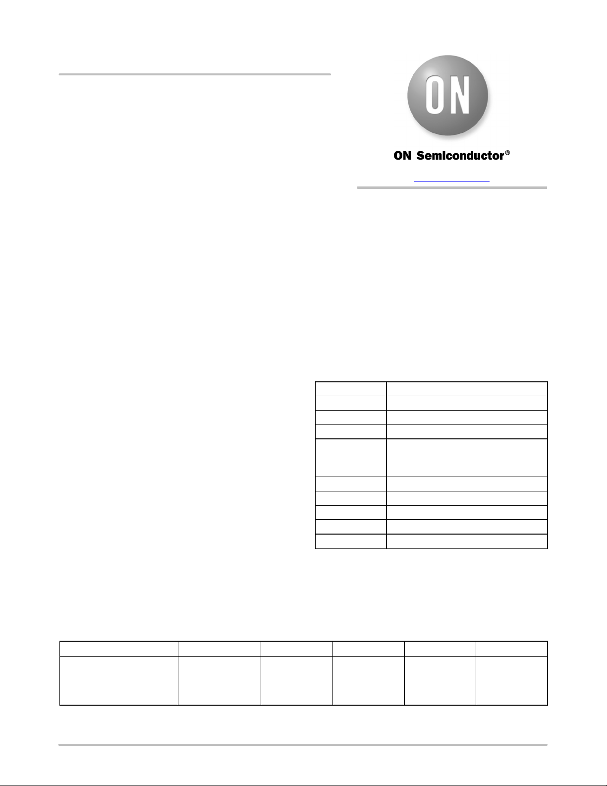
Top View Bottom View
Figure 1. Evaluation Board Photos
CIRCUIT SCHEMATIC
Figure 2. Circuit Schematic
www.onsemi.com
2
Page 3
NCP1568DC48WGEVB
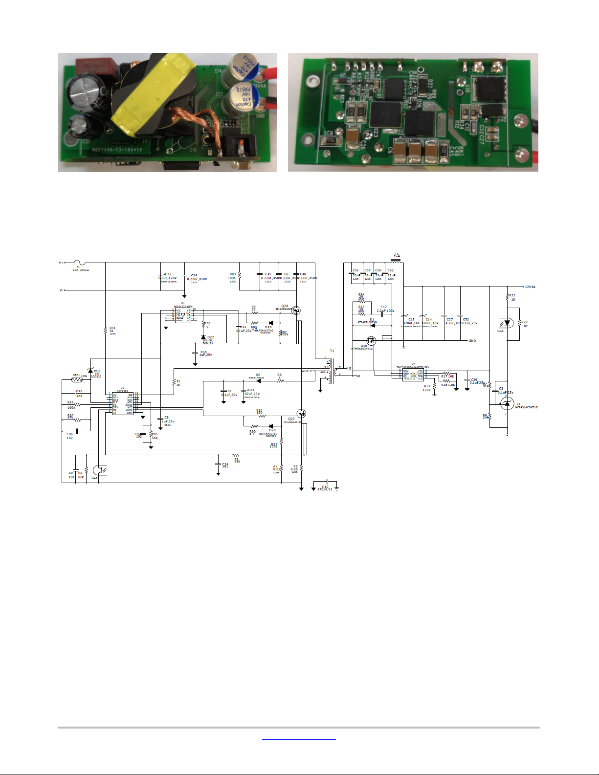
PCB
Figure 3. Top View of Mainboard PCB
Figure 4. Bottom View of Mainboard PCB
www.onsemi.com
3
Page 4
NCP1568DC48WGEVB
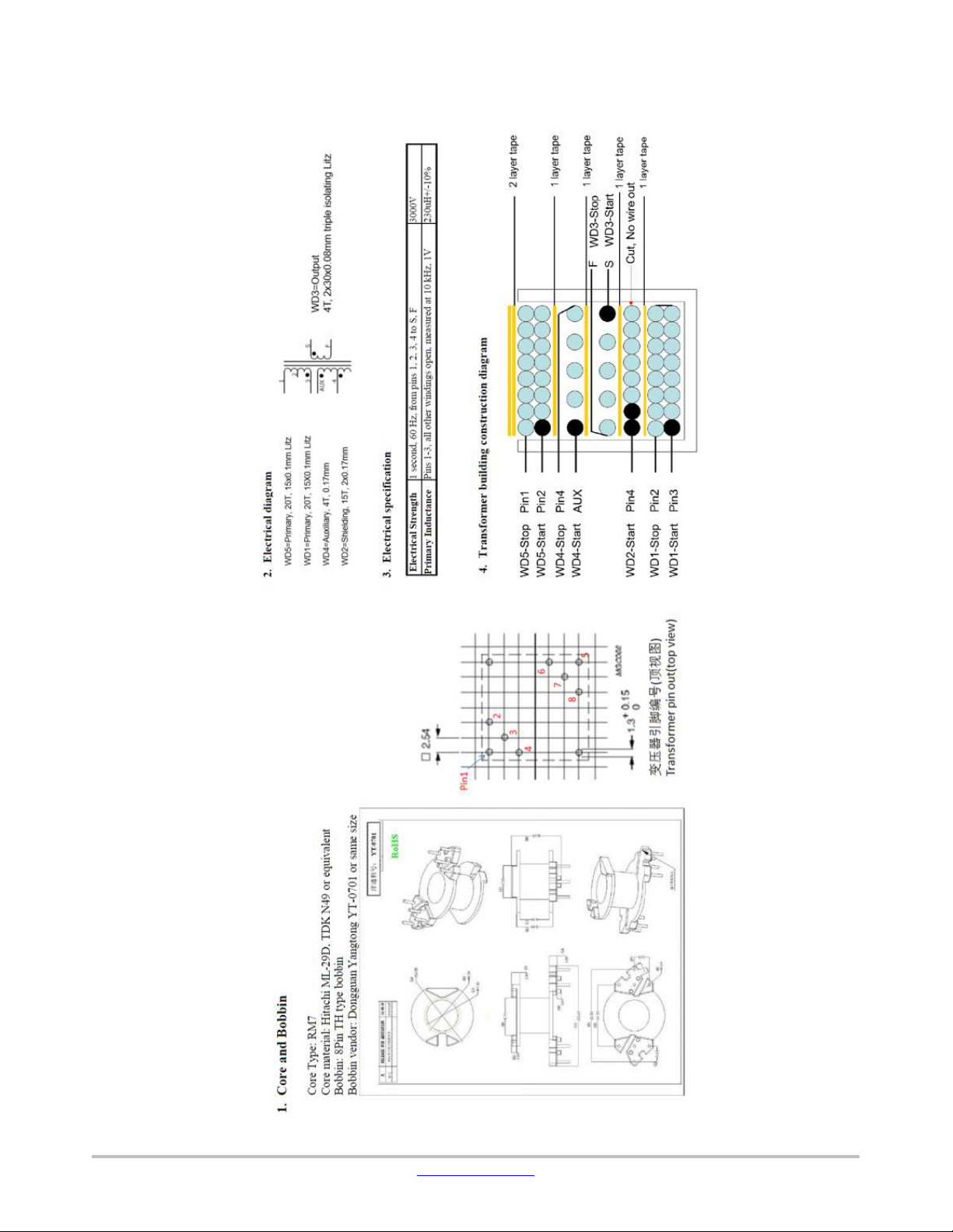
T1 TRANSFORMER DESIGNS
Figure 5.
www.onsemi.com
4
Page 5

NCP1568DC48WGEVB
)
Efficiency
Test Condition: all efficiency are tested at board end
At 75% load At 100% load
95
94
93
92
91
90
89
88
Efficiency(%)
87
86
85
120 160 320 395
Vdc
Figure 6. Efficiency
95
94
93
92
91
90
89
88
Efficiency(%)
87
86
85
120 160 320 395
Vdc
(CH1 Vsw, CH2: Vadrv, CH3: Vsec−drain, CH4: Vsyn−drv)
Figure 7. Startup Waveform at 120 Vdc
120 Vdc (CH1 Vsw, CH2: Vadrv, CH3: Vsec−drain, CH4: Vsyn−drv) 395 Vdc (CH1 Vsw, CH2: Vadrv, CH3: Vsec−drain, CH4: Vsyn−drv
Figure 8. Working Waveform at Full Load
www.onsemi.com
5
Page 6

NCP1568DC48WGEVB
(CH2: Io, CH3: Vsec−drain, CH4: Vo) (CH2: Io, CH3: Vsec−drain, CH4: Vo)
Figure 9. Output Ripple at Full Load
Test condition: 0 − 4 A, 10 ms cycle, 125 mA/ms, 1 m cable,
tested at E−load
Figure 10. Dynamic Test at 160 Vdc
Test condition: 0 − 2 A, 10 ms cycle, 125 mA/ms, 1 m cable,
tested at E−load
www.onsemi.com
6
Page 7

NCP1568DC48WGEVB
(CH2: Io, CH3: Vsec−drain, CH4: Vo) (CH2: Io, CH3: Vsec−drain, CH4: Vo)
395 Vdc input, 500 MHz BW
395 Vdc input, 20 MHz BW
Test condition: 0.1 A − 4.0 A, 10 ms cycle, 125 mA/ms, 1 m cable,
tested at E−load
Figure 11. Dynamic Test at 160 Vdc
(CH2: Vadrv, CH3: Vsec−drain)
Figure 12. Secondary Voltage Stress during DCM to ACF Mode Transition
Test condition: 1 A − 4 A, 10 ms cycle, 125 mA/ms, 1 m cable,
tested at E−load
(CH2: Vadrv, CH3: Vsec−drain)
www.onsemi.com
7
Page 8

NCP1568DC48WGEVB
Table 1. THERMAL IMAGE @ 12 V / 4 A Output
Input
Component Side
Back side
120 Vdc
160 Vdc
www.onsemi.com
8
Page 9

NCP1568DC48WGEVB
320 Vdc
395 Vdc
Table 1. THERMAL IMAGE @ 12 V / 4 A Output (continued)
Input Back sideComponent Side
www.onsemi.com
9
Page 10

NCP1568DC48WGEVB
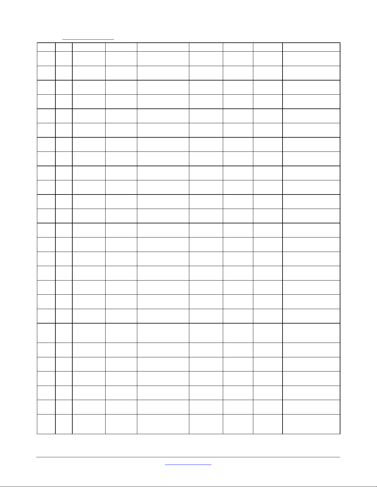
T able 2. BILL OF MATERIAL
Item
Qty
Reference
Type
Part Name
Package
MFR
Value
Description
14C1 C3 C29
Ceramic
/885012105018
402
Wurth
0.1 uF,
Capacitor, Ceramic,
21C52
Ceramic
/885012206071
603
Wurth
0.1 uF,
Capacitor, Ceramic,
34C6 C26
Ceramic
C3225X7T2W224K
1210
TDK
0.22 uF,
Capacitor, Ceramic,
42C9 C34
Ceramic
/885012205055
402
Wurth
101
Capacitor, Ceramic,
51C42
Ceramic
/885012205061
402WE102
Capacitor, Ceramic,
62C46−47
Ceramic
/885012205061
402WE102
Capacitor, Ceramic,
71C8
Ceramic
/885012206076
603
Wurth
1 uF,
Capacitor, Ceramic,
81C43
Ceramic
/885012206076
603WE1 uF,
Capacitor, Ceramic,
91C12
Ceramic
C1608X7R2A222K
603
TDK
2.2 nF,
Capacitor, Ceramic,
104C56−57
Ceramic
C3216X5R1V226M
1206
TDK
22 uF
Capacitor, Ceramic,
111C27
Ceramic
C1608X6S1C475M
603
TDK
4.7 uF,
Capacitor, Ceramic,
121C10
Ceramic
CS65−B2GA101K-
Lead type
TDK
470 pF,
Y Capacitor,safety
131D6
Switching
BAS21HT1G
SOD323
ON
0.2 A,
Swiching diode, 0.2 A,
142D26 D29
Schotty
BAT54XV2T1G
SOD523
ON
0.2 A,
Schotty diode, SMD
151D22
Ultrafast
ES1JFL
SOD123
ON
1 A,
Ultrafast diode, SMD
161D1
Schotty
NTSAF5100T3G
SOD123FL
ON
5 A,
Schotty Rectifier, 5 A,
171F1
Fuse
20T−016H
Axial lead
Hollyfuse
1.6 A,
Micro Fuse, 1.6 A /
181U8
voltage
NCP431ACSNT1G
SOT23
ON
PROGRAMMABLE
191U2
ACF con-
NCP1568S02AD-
TSSOP16
ON
ACF controller
201U7
Syn. recti-
NCP4306AADZZ-
SO8ONSyn. Rectified Con-
211U1
HB driver
NCP51530AMN-
DFN10
ON
HB driver
221NTC1
NTC
SD-
603
Shunlord
100k
replaced by 13k resis-
231U4
Optical
FODM1009
LSOP4
ON
optical coupler, stan-
241L6
SMD In-
/744314200
7050WE2.2 uH
WE−HCI SMD Flat
252R6 R72
Resistor
Std
402
Std1Resistor, Chip, 1/16W,
261R18
Resistor
Std
402
Std
1.8k
Resistor, Chip, 1/16W,
C44
C45 C48
C60 C62
Capacitor
Capacitor
Capcitor
Capacitor
Capacitor
Capacitor
Capacitor
Capacitor
Capacitor
Capcitor
Capacitor
Capcitor
diode
160AC
YNKA
25 V
25 V
450 V
25 V
25 V
100 V
16 V
Y1
250 V
25 V, 10%
25 V, 10%
Chip, 10%
50 V, 10%
50 V, 10%
50 V, 5%
10%
25 V, 10%
SMD, 5%
SMD, 5%
16 V, 10%
standard approved,
10%
250 V
diode
diode
rectifier
reference
troller
fied controller
coupler
ductor
BR2G
ZAMNTWG
TWG
NT1608X104J4250HTF
4X4
30 V
600 V
100 V
250 Vac
100 V
250 V
PRECISION REFERENCE
troller
tor
dard SOP package
Wire High Current Inductor
1%
1%
www.onsemi.com
10
Page 11
T able 2. BILL OF MATERIAL (continued)
273R32
Resistor
Std
402
Std
100k
Resistor, Chip, 1/16W,
281R37
Resistor
Std
402
Std
120k
Resistor, Chip, 1/16W,
291R13
Resistor
Std
402
Std
150
Resistor, Chip, 1/16W,
301R17
Resistor
Std
402
Std
16k
Resistor, Chip, 1/16W,
312R1 R22
Resistor
Std
402
Std1KResistor, Chip, 1/16W,
321R9
Resistor
Std
402
Std22Resistor, Chip, 1/16W,
331R8
Resistor
Std
603
Std
24k
Resistor, Chip, 1/16W,
342R89−90
Resistor
Std
402
Std
4.7
Resistor, Chip, 1/16W,
352R2 R20
Resistor
Std
402
Std
47k
Resistor, Chip, 1/16W,
361R3
Resistor
Std
402
Std
510
Resistor, Chip, 1/16W,
371R45
Resistor
Std
402
Std
56k
Resistor, Chip, 1/16W,
381R7
Resistor
Std
402
Std
91k
Resistor, Chip, 1/16W,
391R29
Resistor
Std
402
StdncResistor, Chip, 1/16W,
401R4
Resistor
ERJ8BQFR062V
1206
Panasonic
0.62
Resistor, Chip, 1/2W,
411R5
Resistor
ERJ8BQFR068V
1206
Panasonic
0.68
Resistor, Chip, 1/2W,
421R31
Resistor
Std
1206
Std1kResistor, Chip, 1/4W,
432R12 R34
Resistor
Std
805
Std20Resistor, Chip, 1/5W,
441R83
Resistor
Std
1206
Std
300K
Resistor, Chip, 1/4W,
451T1
Trans-
RM7
TH type
Wurth
RM7, 8Pin
462C13−14
Electrolyt-
PX471M016E120P
6.3 mm x
CapXon
470 uF,
size: 6.3 mm x 12 mm
471C21
ECAP
KF Series
5 mm x
CapXon
47 uF,
size: 6.3 mm x 11 mm
481C32
ECAP
KF Series
8 mm x
CapXon
6.8 uF,
size: 8 mm x 12 mm
491Q18
MOSFET
NTMFS6B03NT1G
QFN5X6
ON
MOSFET, NChan,
502Q23−24
MOSFET
IPL60R360P6S
ThinkPAK5-
INFINEON
MOSFET, NChan,
511ZD11
zener
MM3Z11VT1G
SOD323
ON
16v
GENERIC ZENER−
52412V4A
connec-
Std
Ø1mm
Std
connection ternimal or
Item DescriptionValueMFRPackagePart NameTypeReferenceQty
NCP1568DC48WGEVB
R91−92
1%
1%
1%
1%
1%,
1%
1%
1%
1%
1%
1%
1%
1%,
GND V+
V−
former
ic solid
capacitor
tion ternimal
12 mm
11 mm
12 mm
X6
1%
1%
1%
1%
1%
16 V
25 V
420 V
100 V
600 V
DIODE
wire
www.onsemi.com
11
Page 12

NCP1568DC48WGEVB
References
ON Semiconductor datasheet for NCP1568, NCP51530, NCP4306, NTMFS6B03
ON Semiconductor Design Notes DN05043
www.onsemi.com
12
Page 13

ON Semiconductor and the ON Semiconductor logo are trademarks of Semiconductor Components Industries, LLC dba ON Semiconductor or its subsidiaries in the United States and/or
other countries. ON Semiconductor owns the rights to a number of patents, trademarks, copyrights, trade secrets, and other intellectual property. A listing of ON Semiconductor’s
product/patent coverage may be accessed at www.onsemi.com/site/pdf/Patent−Marking.pdf
subject to all applicable copyright laws and is not for resale in any manner.
The evaluation board/kit (research and development board/kit) (hereinafter the “board”) is not a finished product and is as such not available for sale to consumers. The board is only intended
for research, development, demonstration and evaluation purposes and should as such only be used in laboratory/development areas by persons with an engineering/technical training
and familiar with the risks associated with handling electrical/mechanical components, systems and subsystems. This person assumes full responsibility/liability for proper and safe handling.
Any other use, resale or redistribution for any other purpose is strictly prohibited.
The board is delivered “AS IS” and without warranty of any kind including, but not limited to, that the board is production−worthy, that the functions contained in the board will meet your
requirements, or that the operation of the board will be uninterrupted or error free. ON Semiconductor expressly disclaims all warranties, express, implied or otherwise, including without
limitation, warranties of fitness for a particular purpose and non−infringement of intellectual property rights.
ON Semiconductor reserves the right to make changes without further notice to any board.
You are responsible for determining whether the board will be suitable for your intended use or application or will achieve your intended results. Prior to using or distributing any systems
that have been evaluated, designed or tested using the board, you agree to test and validate your design to confirm the functionality for your application. Any technical, applications or design
information or advice, quality characterization, reliability data or other services provided by ON Semiconductor shall not constitute any representation or warranty by ON Semiconductor,
and no additional obligations or liabilities shall arise from ON Semiconductor having provided such information or services.
The boards are not designed, intended, or authorized for use in life support systems, or any FDA Class 3 medical devices or medical devices with a similar or equivalent classification in
a foreign jurisdiction, or any devices intended for implantation in the human body. Should you purchase or use the board for any such unintended or unauthorized application, you shall
indemnify and hold ON Semiconductor and its officers, employees, subsidiaries, affiliates, and distributors harmless against all claims, costs, damages, and expenses, and reasonable
attorney fees arising out of, directly or indirectly, any claim of personal injury or death associated with such unintended or unauthorized use, even if such claim alleges that ON Semiconductor
was negligent regarding the design or manufacture of the board.
This evaluation board/kit does not fall within the scope of the European Union directives regarding electromagnetic compatibility, restricted substances (RoHS), recycling (WEEE), FCC,
CE or UL, and may not meet the technical requirements of these or other related directives.
FCC WARNING – This evaluation board/kit is intended for use for engineering development, demonstration, or evaluation purposes only and is not considered by ON Semiconductor to
be a finished end product fit for general consumer use. It may generate, use, or radiate radio frequency energy and has not been tested for compliance with the limits of computing devices
pursuant to part 15 of FCC rules, which are designed to provide reasonable protection against radio frequency interference. Operation of this equipment may cause interference with radio
communications, in which case the user shall be responsible, at its expense, to take whatever measures may be required to correct this interference.
ON Semiconductor does not convey any license under its patent rights nor the rights of others.
LIMITATIONS OF LIABILITY: ON Semiconductor shall not be liable for any special, consequential, incidental, indirect or punitive damages, including, but not limited to the costs of
requalification, delay, loss of profits or goodwill, arising out of or in connection with the board, even if ON Semiconductor is advised of the possibility of such damages. In no event shall
ON Semiconductor’s aggregate liability from any obligation arising out of or in connection with the board, under any theory of liability, exceed the purchase price paid for the board, if any.
For more information and documentation, please visit www.onsemi.com
.
. ON Semiconductor is an Equal Opportunity/Affirmative Action Employer. This literature is
PUBLICATION ORDERING INFORMATION
LITERATURE FULFILLMENT:
Email Requests to: orderlit@onsemi.com
ON Semiconductor Website: www.onsemi.com
TECHNICAL SUPPORT
North American Technical Support:
Voice Mail: 1 800−282−9855 Toll Free USA/Canada
Phone: 011 421 33 790 2910
Europe, Middle East and Africa Technical Support:
Phone: 00421 33 790 2910
For additional information, please contact your local Sales Representative
◊
www.onsemi.com
1
 Loading...