

Page 1
EVBUM2776/D
Specifications
Output Voltage
5, 9, 12, 15, 20 V
Ripple
< 2%
Nominal Current
3 A / 2.25 A @ 20 V
Max Current
3 A / 2.25 A @ 20 V
Min Current
Zero
Device
Application
Input Voltage
Output Power
Topology
I/O Isolation
NCP1568D
PoE to USB−PD
37 Vdc − 57 Vdc
45 W
Active Clamp
Isolated
NCP1568D PoE Input
USB-PD Evaluation Board
User's Manual
Circuit Description
This evaluation board manual describes a 45 W universal
input 5 V, 9 V, 15 V and 20 V output evaluation board for
Power over Ethernet to USB−PD applications. This featured
power supply is an active−clamp flyback topology utilizing
ON Semiconductor’s NCP1568D PWM controller,
NCP51530 HB Driver, NCP4308 SR Controller and
FUSB3307 USB−PD Controller . This design note provides
complete circuit schematic, PCB, BOM and transformer
information of the evaluation board. It also provide
efficiency, transient response, output ripple and thermal data
of the evaluation board.
This design utilized NCP1568 and NCP51530 for the
active clamp flyback topology. Active clamp flyback
topology effectively recycles the leakage energy. Another
feature of this topology is the ZVS operation of the power
MOSFETS. Because of no leakage losses and ZVS
operation, this topology is suited for high frequency
operation which results in size reduction of the transformer.
Hence Active clamp flyback topology is well suited for high
power density sub 100 W power supplies.
NCP1568D is a highly integrated DC−DC PWM
controller designed to implement an active clamp flyback
topology. It features adaptive frequency scheme which
optimizes frequency of operation and hence the efficiency
over all load and input voltages. The NCP1568 features a
HV startup circuit.
NCP51530 is a 700 V high side and low side driver with
2 A current drive capability for DC−DC power supplies and
inverters. NCP51530 offers best in class propagation delay,
low quiescent current and low switching current at high
frequencies of operation. This device is tailored for highly
efficient power supplies operating at high frequencies.
NCP4308 is high performance driver tailored to control a
synchronous rectification MOSFET in switch mode power
supplies.
www.onsemi.com
EVAL BOARD USER’S MANUAL
FUSB3307 is a fully compliant, highly integrated USB
Power Delivery (PD) power source controller that can
control a DC−DC port power regulator or the opto−coupler
in the secondary side of an AC−DC adapter.
Key Features
• PoE Compatible DC−DC Input Voltages (37 V – 57 V)
• High Full Load and Average Efficiency
• Low Standby Power
• Very Low Ripple and Noise
• High Frequency Operation up to 400 kHz
• Thermal and OVP Protection
• Adaptive Frequency Operation based on Input and
Output Load Conditions
• Adaptive ZVS Operation
• Inherent SCP and OCP Protection
• Board Dimensions: 2.23” x 1.34” x 0.58”
NCP51530
NCP4308D
FUSB3307
FDMS86255
FDMS86101
© Semiconductor Components Industries, LLC, 2020
November, 2020 − Rev. 0
Adapter
Flyback
1 Publication Order Number:
EVBUM2776/D
Page 2
EVBUM2776/D
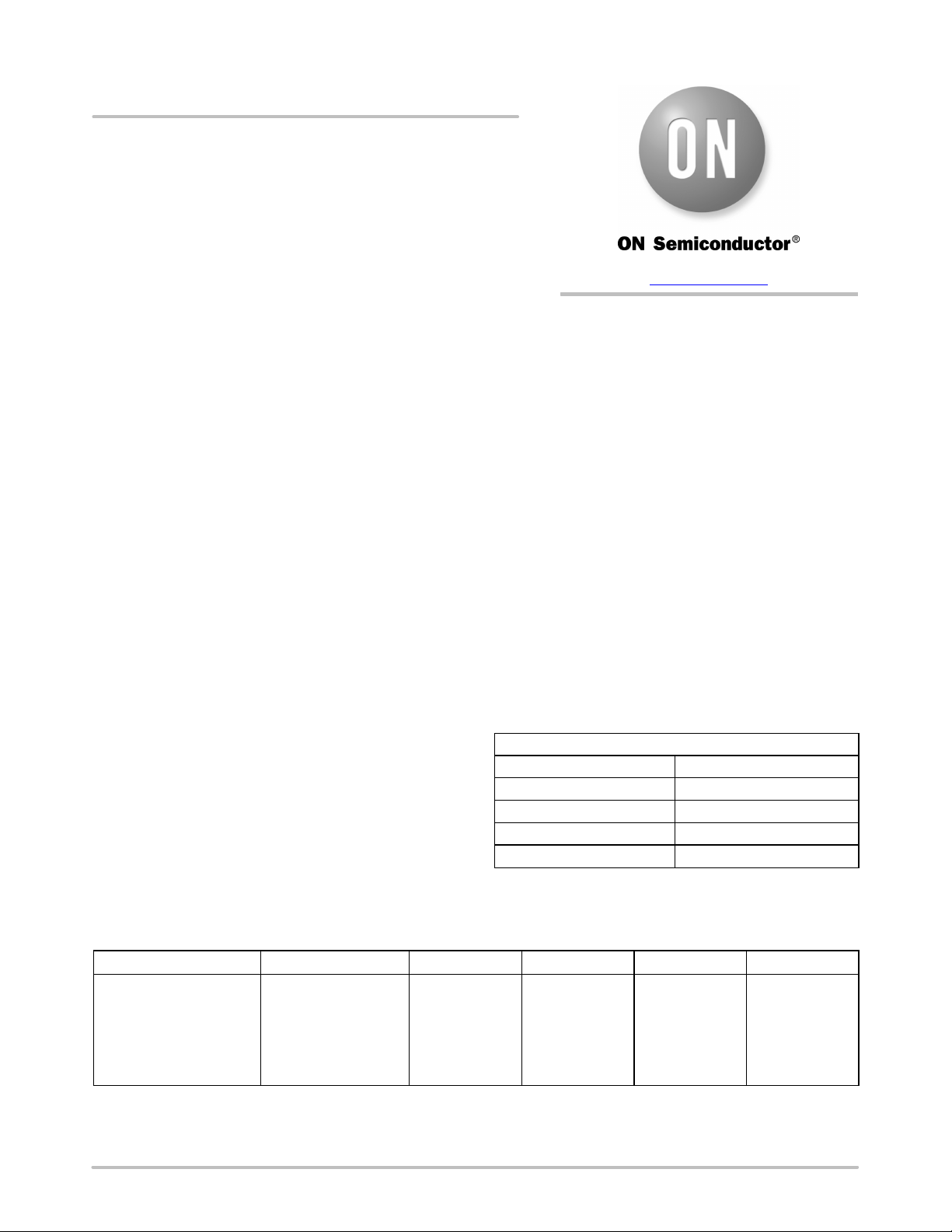
Figure 1. Top View of the Evaluation Board
Figure 2. Full View of the Evaluation Board
Figure 3. View of the Daughter Card
www.onsemi.com
2
Page 3
EVBUM2776/D
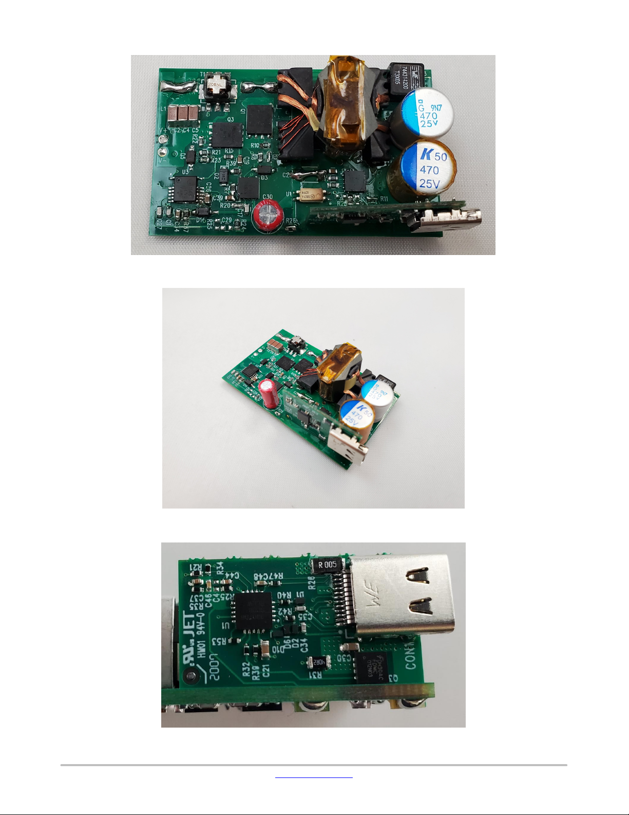
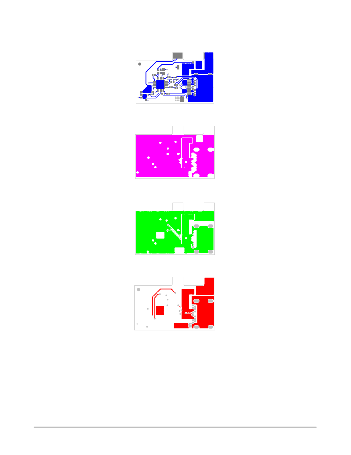
MAIN BOARD LAYOUT
Figure 4. Main Board Top Layer
Figure 5. Main Board Inner Layer 1
www.onsemi.com
3
Page 4
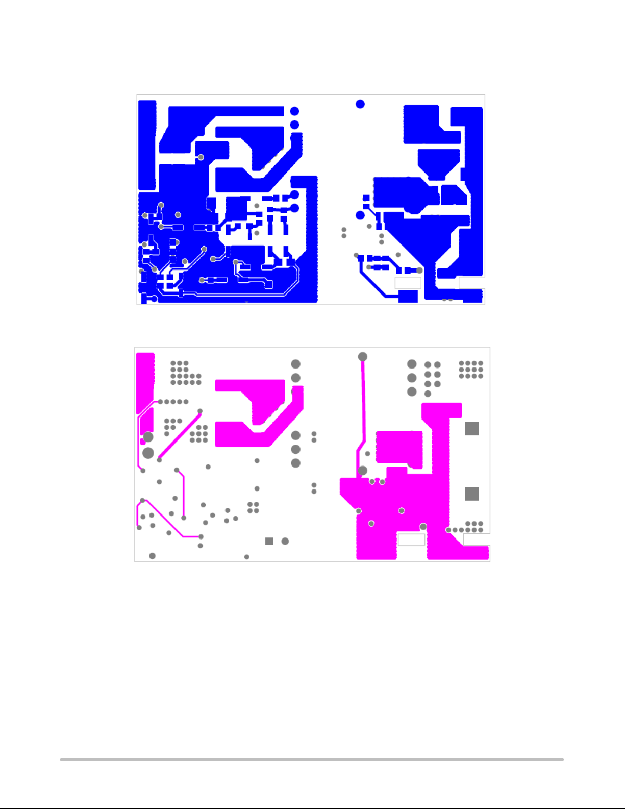
EVBUM2776/D
Figure 6. Main Board Inner Layer 2
Figure 7. Main Board Bottom Layer
www.onsemi.com
4
Page 5
EVBUM2776/D
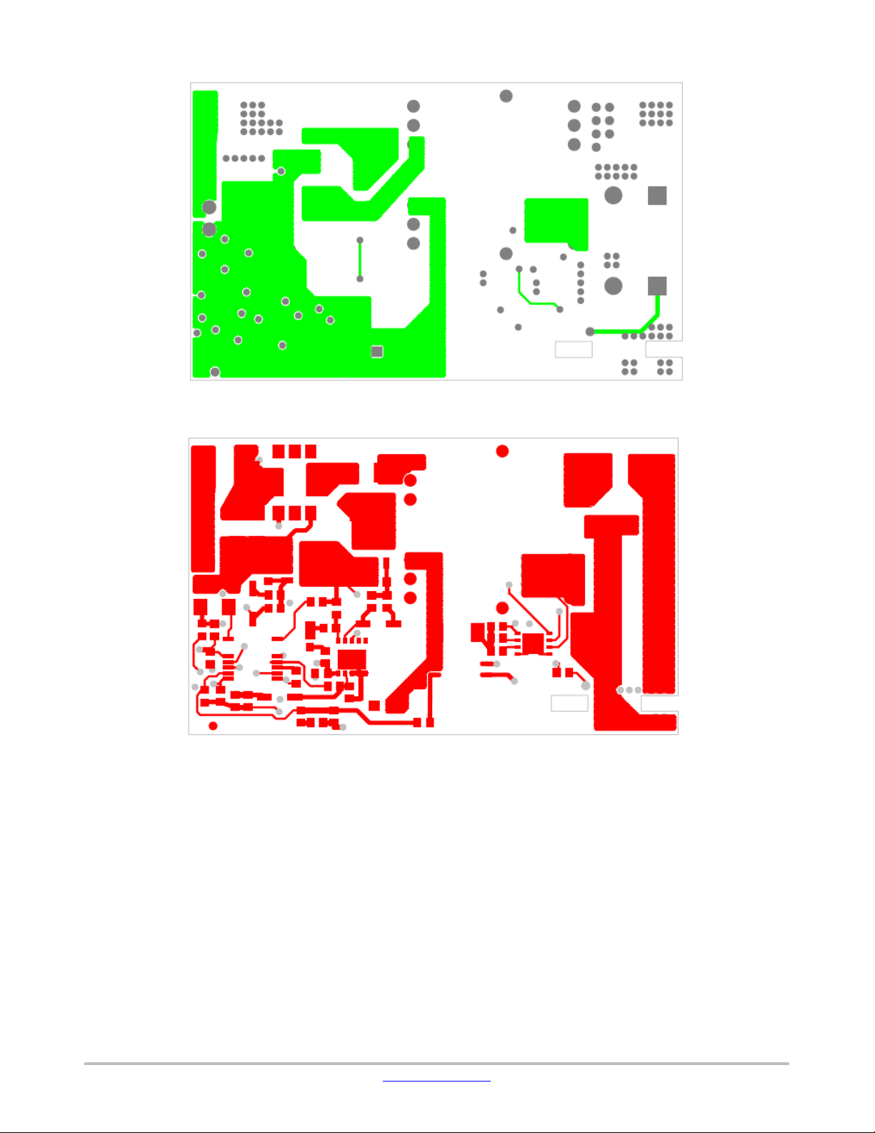
DAUGHTER BOARD LAYOUT
Figure 8. Daughter Card Top Layer
Figure 9. Daughter Card Inner Layer 1
Figure 10. Daughter Card Inner Layer 2
Figure 11. Daughter Card Bottom Layer
www.onsemi.com
5
Page 6
EVBUM2776/D
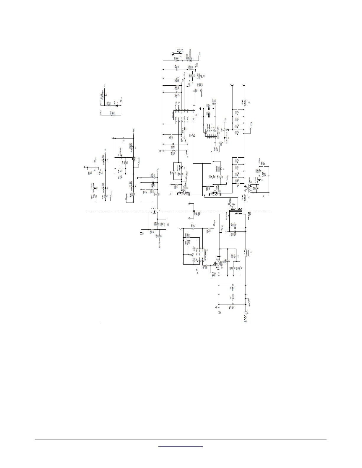
MAIN BOARD SCHEMATIC
Figure 12. Main Board Schematic
www.onsemi.com
6
Page 7
EVBUM2776/D
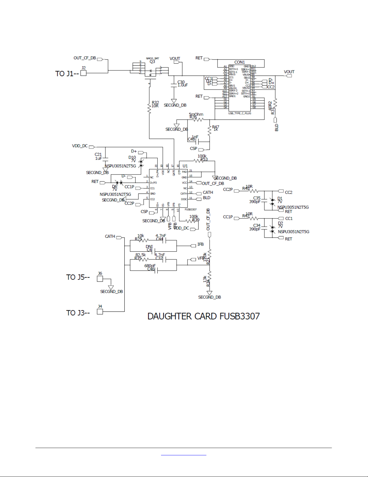
DAUGHTER BOARD SCHEMATIC
Figure 13. Daughter Card Schematic
www.onsemi.com
7
Page 8
EVBUM2776/D
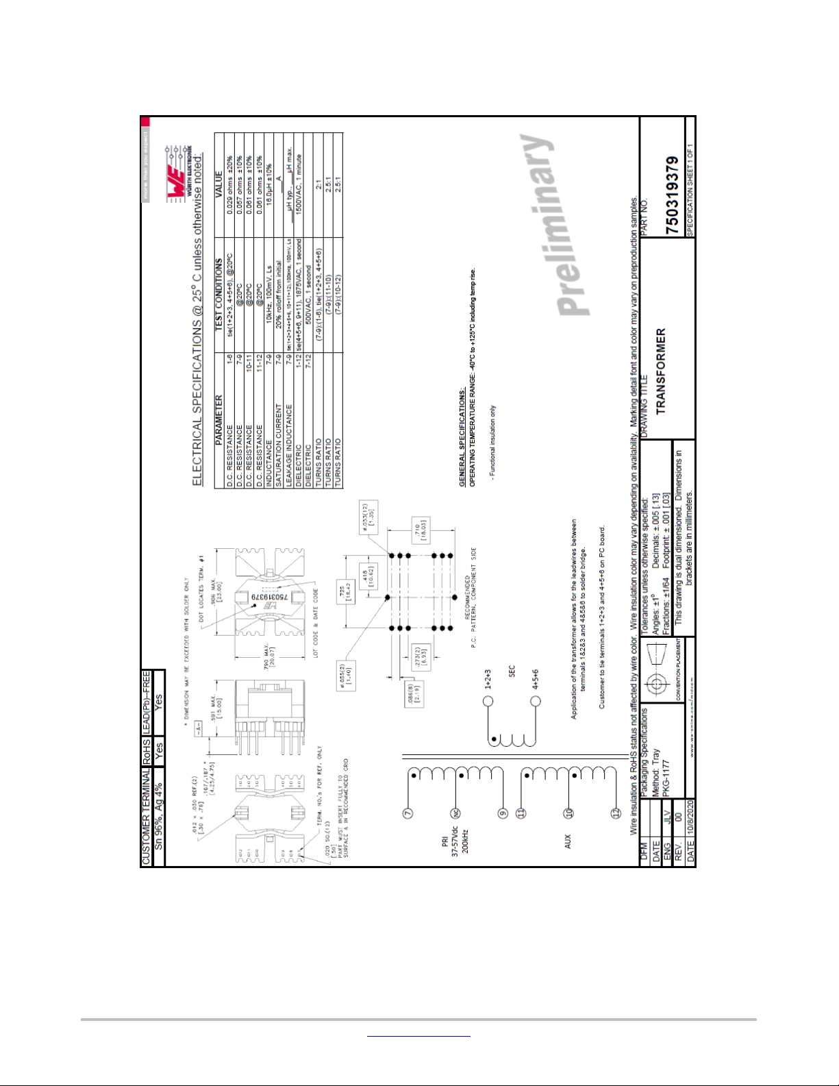
MAGNETIC DESIGN
Figure 14. Transformer Design (Core: Hitachi ML29D)
www.onsemi.com
8
Page 9
Evaluation Board Efficiency Data
Efficiency (%)
15 V Output Efficiency vs. Load
V
V
V
100%
95%
90%
85%
EVBUM2776/D
20 V Output Efficiency vs. Load
Efficiency (%)
100%
80%
75%
70%
65%
60%
0 0.25 0.5 0.75 1 1.25 1.5 1.75 2 2.25
Output Current (A)
Figure 15. 20 V Efficiency Plot
95%
90%
85%
37 V
48 V
57 V
80%
75%
70%
65%
60%
0 0.5 1 1.5 2 2.5 3
Output Current (A)
Figure 16. 15 V Efficiency Plot
www.onsemi.com
9
37
48
57
Page 10
100%
95%
90%
85%
EVBUM2776/D
12 V Output Efficiency vs. Load
Efficiency (%)
100%
80%
75%
70%
65%
60%
0 0.5 1 1.5 2 2.5 3
Output Current (A)
Figure 17. 12 V Efficiency Plot
9 V Output Efficiency vs. Load
95%
90%
85%
37 V
48 V
57 V
Efficiency (%)
80%
75%
70%
65%
60%
0 0.5 1 1.5 2 2.5 3
Output Current (A)
Figure 18. 9 V Efficiency Plot
www.onsemi.com
10
37 V
48 V
57 V
Page 11
100%
95%
90%
85%
EVBUM2776/D
5 V Output Efficiency vs. Load
Efficiency (%)
80%
75%
70%
65%
60%
0 0.5 1 1.5 2 2.5 3
Output Current (A)
Figure 19. 5 V Efficiency Plot
OUTPUT RIPPLE
37 V
48 V
57 V
Figure 20. 37 Vin 5 Vout Output Ripple
www.onsemi.com
11
Page 12

EVBUM2776/D
Figure 21. 48 Vin 5 Vout Output Ripple
Figure 22. 57 Vin 5 Vout Output Ripple
www.onsemi.com
12
Page 13

EVBUM2776/D
Figure 23. 37 Vin 9 Vout Output Ripple
Figure 24. 48 Vin 9 Vout Output Ripple
www.onsemi.com
13
Page 14

EVBUM2776/D
Figure 25. 57 Vin 9 Vout Output Ripple
Figure 26. 37 Vin 12 Vout Output Ripple
www.onsemi.com
14
Page 15

EVBUM2776/D
Figure 27. 48 Vin 12 Vout Output Ripple
Figure 28. 57 Vin 12 Vout Output Ripple
www.onsemi.com
15
Page 16

EVBUM2776/D
Figure 29. 37 Vin 15 Vout Output Ripple
Figure 30. 48 Vin 15 Vout Output Ripple
www.onsemi.com
16
Page 17

EVBUM2776/D
Figure 31. 57 Vin 15 Vout Output Ripple
Figure 32. 37 Vin 20 Vout Output Ripple
www.onsemi.com
17
Page 18

EVBUM2776/D
Figure 33. 48 Vin 20 Vout Output Ripple
Figure 34. 57 Vin 20 Vout Output Ripple
www.onsemi.com
18
Page 19

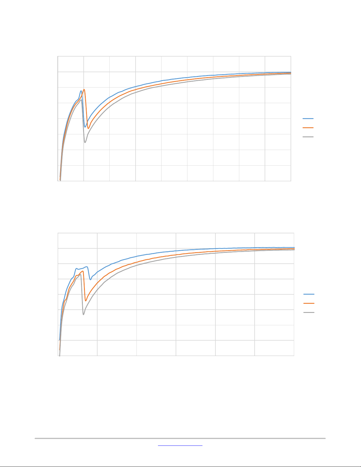
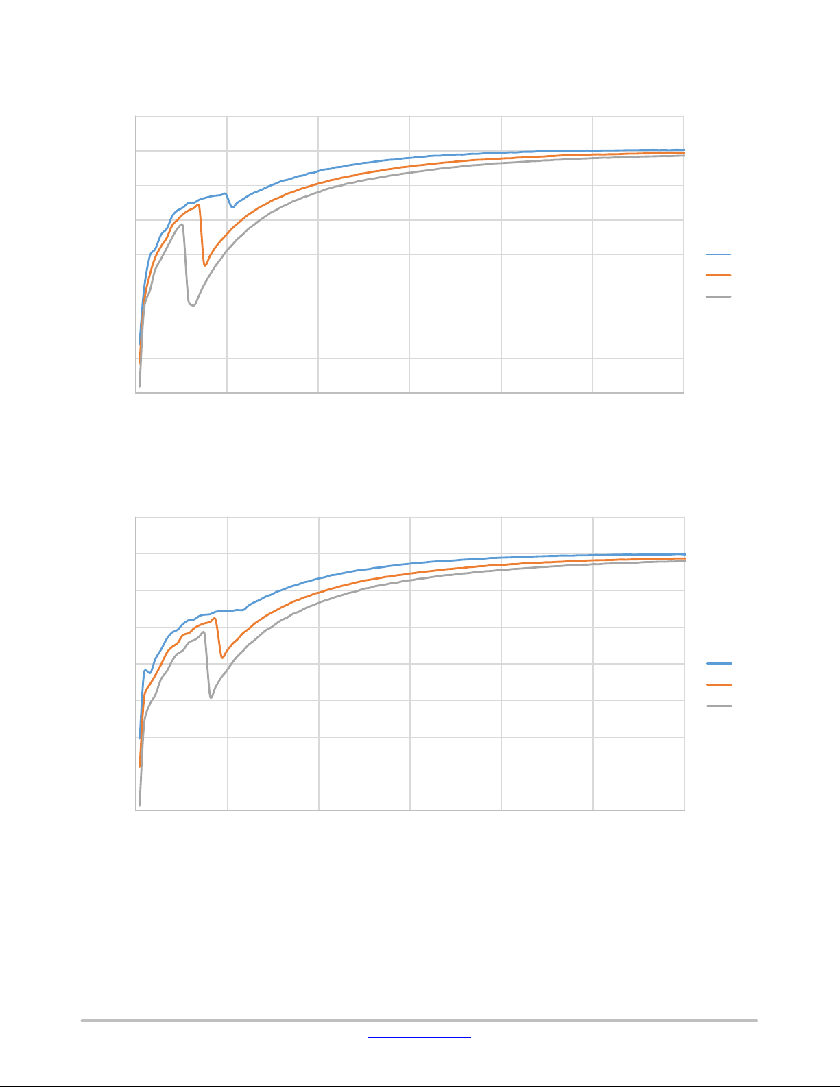
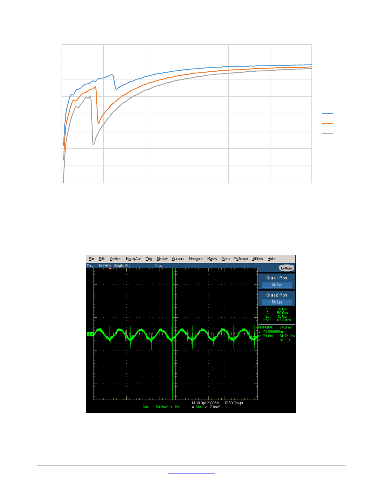
Transient Response
(0.1 A − 3A / 2.25 A, 150 mA/ms, 20 ms)
EVBUM2776/D
Figure 35. 37 Vin 5 Vout Transient Response
Figure 36. 48 Vin 5 Vout Transient Response
www.onsemi.com
19
Page 20

EVBUM2776/D
Figure 37. 57 Vin 5 Vout Transient Response
Figure 38. 37 Vin 9 Vout Transient Response
www.onsemi.com
20
Page 21

EVBUM2776/D
Figure 39. 48 Vin 9 Vout Transient Response
Figure 40. 57 Vin 9 Vout Transient Response
www.onsemi.com
21
Page 22

EVBUM2776/D
Figure 41. 37 Vin 12 Vout Transient Response
Figure 42. 48 Vin 12 Vout Transient Response
www.onsemi.com
22
Page 23

EVBUM2776/D
Figure 43. 57 Vin 12 Vout Transient Response
Figure 44. 37 Vin 15 Vout Transient Response
www.onsemi.com
23
Page 24

EVBUM2776/D
Figure 45. 48 Vin 15 Vout Transient Response
Figure 46. 57 Vin 15 Vout Transient Response
www.onsemi.com
24
Page 25

EVBUM2776/D
Figure 47. 37 Vin 20 Vout Transient Response
Figure 48. 48 Vin 20 Vout Transient Response
www.onsemi.com
25
Page 26

EVBUM2776/D
Thermal Data
All T emperatures shown in °Celsius
Figure 49. 57 Vin 20 Vout Transient Response
SRFET 64.10
Figure 50. 37 Vin 15 Vout Full Load Top
www.onsemi.com
26
Page 27

EVBUM2776/D
Transformer Winding LFET HFET NCP1568 NCP51530 NCP4308
73.83 78.14 52.3 56.48 47.02 47.65 56.74
Figure 51. 37 Vin 15 Vout Full Load Bottom
SRFET 66.17
Figure 52. 48 Vin 15 Vout Full Load Top
www.onsemi.com
27
Page 28

EVBUM2776/D
Transformer Winding LFET HFET NCP1568 NCP51530 NCP4308
77.33 80.71 55.26 59.35 51.57 52.42 58.95
Figure 53. 48 Vin 15 Vout Full Load Bottom
SRFET 66.92
Figure 54. 57 Vin 15 Vout Full Load Top
www.onsemi.com
28
Page 29

EVBUM2776/D
Transformer Winding LFET HFET NCP1568 NCP51530 NCP4308
79.95 82.84 57.88 61.58 54.04 55.69 60.25
Figure 55. 57 Vin 15 Vout Full Load Bottom
SRFET 62.38
Figure 56. 37 Vin 20 Vout Full Load Top
www.onsemi.com
29
Page 30

EVBUM2776/D
Transformer Winding LFET HFET NCP1568 NCP51530 NCP4308
75.15 78.23 54.72 57.96 51.85 51.96 58.93
Figure 57. 37 Vin 20 Vout Full Load Bottom
SRFET 64.47
Figure 58. 48 Vin 20 Vout Full Load Top
www.onsemi.com
30
Page 31

EVBUM2776/D
Transformer Winding LFET HFET NCP1568 NCP51530 NCP4308
79.47 81.8 56.28 60.44 53.95 54.32 61.87
Figure 59. 48 Vin 20 Vout Full Load Bottom
SRFET 66.49
Figure 60. 57 Vin 20 Vout Full Load Top
www.onsemi.com
31
Page 32

EVBUM2776/D
Transformer Winding LFET HFET NCP1568 NCP51530 NCP4308
83.12 84.65 57.74 61.94 55.61 56.19 64.02
Figure 61. 57 Vin 20 Vout Full Load Bottom
www.onsemi.com
32
Page 33

EVBUM2776/D
Table 1. BILL OF MATERIALS MAIN BOARD
Qty
Reference
Manufacturer
Manufacturer Part Number
Voltage
Value
Footprint
1Q4ON Semiconductor
2N7002
60 V
SOT−23
1
C19
Wurth Electronik
885012206095
50 V
0.1 mF
603
3
C21 C26 C39
TDK
CGA3E3X5R1H105K080AB
50 V
1.0 mF
603
2
C24 C34
Wurth Electronik
885012206095
50 V
120 nF
603
1
C27
Wurth Electronik
885012006058
50 V
120 pF
603
1
C23
Wurth Electronik
885012006029
16 V
1 nF
603
1
C28
Wurth Electronik
885012206085
50 V
2.2 nF
603
1
C12
Wurth Electronik
885342006005
250 V
470 pF
603
2
C1 C17
Wurth Electronik
885012006021
16 V
47 pF
603
1
C29
DNI
603
2
C37 C40−41
Wurth Electronik
885012207103
50 V
1 mF
805
1
C38
Taiyo Yuden
GMK325BJ226MM−P
22 mF
1206
7
C2−8
Murata
GRM31CC72A475KE11L
100 V
4.7 mF
1206
1C9Murata
GRM31CC72A475KE11L
DNI
1206
1
C16
STD
100 pF
1210
3
C10−11 C15
Taiyo Yuden
GMK325BJ226MM−P
22 mF
1206
1
C20
Wurth Electronik
8853622100091
470 pF
1808
1
C30
Wurth Electronik
860020673014
50 V
68 mF
(6.3)mm
2
C13 C14
Kemet
A750MS477M1EAAE015
470 mF
TH−10x5mm
3
J19 J30−31NANA
NA
2X3mm
6
D7−8 D10−12
ON Semiconductor
MMSD4148T3G
100 V
SOD−123
1D2Vishay
VS−1EQH02−M3/H
200 V
DO−219AD
5
D1 D3 D5−6
ON Semiconductor
MBR0530
30 V
SOD−123
1D4ON Semiconductor
MMSZ5250BT1G
20 V
SOD 123
1D9ON Semiconductor
MM3Z16VT1G
16 V
SOD−323
1
D13
ON Semiconductor
6.8 V
SOD−323
1U1CEL
FODM8801BV
80 V
1.17 V 50 mA
4−SMD, Gull
1T2Wurth Electronik
7.5E+08
16uH Hitachi
RM6 12pin
3
L1−3
SHORT
1U3ON Semiconductor
NCP1568C
30 V 1 MHz
TSSOP−16_SPE
1U2ON Semiconductor
NCP4308DMNTWG
DFN8−TPAD
1U6ON Semiconductor
NCP51530AMNTWG
NCP51530AM
DGN−10 W/PAD
2
Q1 Q3
ON Semiconductor
FDMS86255
150 V
PWR56
1Q2ON Semiconductor
FDMS86101
100 V
PWR56
2
R9 R26
Vishay
CRCW06030000Z0BC
0
603
2
R12 R20
Vishay
CRCW06030000Z0BC
0
603
2
R7 R11
Vishay
CRCW06031R00JNEA
1
603
1
R23
Vishay
CRCW060310R0JNEA
10
603
1R3Vishay
CRCW0603100RFKEA
100
603
1
R18
Vishay
CRCW0603100KFKEA
100k
603
Rating
D14
D15
Wing
ML29D Core
CIAL
NTWG
www.onsemi.com
33
Page 34

EVBUM2776/D
1
R13
Vishay
CRCW060310K0JNEA
10k
603
1R2Vishay
CRCW060311R0FKEA
11R0
603
1
R21
Yageo
RC0603FR−0715RL
15
603
1
R37
Vishay
CRCW060316K2FKEA
16.2k
603
1
R15
Yageo
RT0603FRE071KL
1k
603
1
R29
Vishay
CRCW06032K00FKEA
2.00k
603
1
R42
Vishay
CRCW06032M49FKEA
2.49M
603
2
R16−17
Vishay
CRCW06032K49FKEAC
2.49k
603
1
R30
Vishay
CRCW060320R0FKEA
20
603
1
R24
Panasonic
ERJ−3EKF4532V
30.9k
6031R1
Vishay
CRCW0603324RFKEA
324R
603
1
R27
Vishay
CRCW060338K3FKEA
38.3k
603
1
R38
Yageo
RC0603FR−074K99L
4.99k
6031R8
Vishay
CRCW060343R0JNEA
43
603
1
R19
Vishay
CRCW060344K2FKEA
44.2k
603
1
R41
Vishay
CRCW0603475KFKEA
475k
603
2
R10 R22
Vishay
CRCW060347K0JNEA
47k
603
3
R31−32 R40
Vishay
??
4R99
603
1
R33
DNI
603
1
R39
Vishay
CRCW06031R00JNEA
DNI
603
2
R34−35
DNI
603
2
R25 R28????
DNI
603
2
R6 R14
Vishay
CRCW1206100RJNEA
100
12061R4
Vishay
20k
1206
1R5Vishay
DNI
1206
1T1Wurth
7.5E+08
1:100
SMD−8.4x7.2mm
Table 1. BILL OF MATERIALS MAIN BOARD (continued)
Voltage
Qty FootprintValue
Manufacturer Part NumberManufacturerReference
Rating
www.onsemi.com
34
Page 35

EVBUM2776/D
Table 2. BILL OF MATERIALS DAUGHTER CARD
Qty
Reference
Manufacturer
Manufacturer Part Number
Voltage Rating
Value
Footprint
1
C46
Kemet
C0402C681G5GACTU
25 V
680 pF
4021C4
25 V
DNI
402
2
C37 C44
TDK
CGA2B2X7R1H472K050BE
50 V
4.7 nF
402
1
C30
Samsung
CL10A105KL8NNNC
35 V
1.0 mF
6031R32
Vishay
CRCW040210R0FKED
10R
402
1
R21
Vishay
CRCW0402120KJNED
120k
4021R34
Vishay
CRCW040213K0JNED
13k
402
2
R40 R42
Vishay
CRCW040210R0FKED
10R
4021R39
Yageo
RC0402FR−07100KL
100k
402
1
R53
Yageo
RC0402FR−07100KL
100k
402
1
R25
Vishay
CRCW040210K0FKEDC
10k
4021R35
Vishay
CRCW040282K5FKEDC
82.5k
402
1
R47
Vishay
CRCW04021K00FKTD
1k
402
3
J2 J4 J6NANA
NA
2x3 mm1U1
ON Semiconductor
FUSB3307
QFNW20
1
C48
Yageo
CC0402JRX7R9BB102
50 V
1 nF
402
2
C34−35
Murata
GRM1555C1H391JA01J
50 V
390 pF
4021Q3
ON Semiconductor
FDMC012N03
Power33
1
R31
Yageo
AC0805FR−0740R2L
40R2
805
4
D1−2 D6 D10
ON Semiconductor
NSPU3051N2T5G
7V
X2DFN2
1
C21
AVX
0603DD105KAT2A
35 V
1 mF
603
1
CON1
Wurth
632723300011
NA
THT/SM
1
R26
Visahy
WSLP12065L000FEA
5 m
1206
W
www.onsemi.com
35
Page 36

ON Semiconductor and the ON Semiconductor logo are trademarks of Semiconductor Components Industries, LLC dba ON Semiconductor or its subsidiaries in the United States and/or
other countries. ON Semiconductor owns the rights to a number of patents, trademarks, copyrights, trade secrets, and other intellectual property. A listing of ON Semiconductor’s
product/patent coverage may be accessed at www.onsemi.com/site/pdf/Patent−Marking.pdf
subject to all applicable copyright laws and is not for resale in any manner.
The evaluation board/kit (research and development board/kit) (hereinafter the “board”) is not a finished product and is as such not available for sale to consumers. The board is only intended
for research, development, demonstration and evaluation purposes and should as such only be used in laboratory/development areas by persons with an engineering/technical training
and familiar with the risks associated with handling electrical/mechanical components, systems and subsystems. This person assumes full responsibility/liability for proper and safe handling.
Any other use, resale or redistribution for any other purpose is strictly prohibited.
The board is delivered “AS IS” and without warranty of any kind including, but not limited to, that the board is production−worthy, that the functions contained in the board will meet your
requirements, or that the operation of the board will be uninterrupted or error free. ON Semiconductor expressly disclaims all warranties, express, implied or otherwise, including without
limitation, warranties of fitness for a particular purpose and non−infringement of intellectual property rights.
ON Semiconductor reserves the right to make changes without further notice to any board.
You are responsible for determining whether the board will be suitable for your intended use or application or will achieve your intended results. Prior to using or distributing any systems
that have been evaluated, designed or tested using the board, you agree to test and validate your design to confirm the functionality for your application. Any technical, applications or design
information or advice, quality characterization, reliability data or other services provided by ON Semiconductor shall not constitute any representation or warranty by ON Semiconductor,
and no additional obligations or liabilities shall arise from ON Semiconductor having provided such information or services.
The boards are not designed, intended, or authorized for use in life support systems, or any FDA Class 3 medical devices or medical devices with a similar or equivalent classification in
a foreign jurisdiction, or any devices intended for implantation in the human body. Should you purchase or use the board for any such unintended or unauthorized application, you shall
indemnify and hold ON Semiconductor and its officers, employees, subsidiaries, affiliates, and distributors harmless against all claims, costs, damages, and expenses, and reasonable
attorney fees arising out of, directly or indirectly, any claim of personal injury or death associated with such unintended or unauthorized use, even if such claim alleges that ON Semiconductor
was negligent regarding the design or manufacture of the board.
This evaluation board/kit does not fall within the scope of the European Union directives regarding electromagnetic compatibility, restricted substances (RoHS), recycling (WEEE), FCC,
CE or UL, and may not meet the technical requirements of these or other related directives.
FCC WARNING – This evaluation board/kit is intended for use for engineering development, demonstration, or evaluation purposes only and is not considered by ON Semiconductor to
be a finished end product fit for general consumer use. It may generate, use, or radiate radio frequency energy and has not been tested for compliance with the limits of computing devices
pursuant to part 15 of FCC rules, which are designed to provide reasonable protection against radio frequency interference. Operation of this equipment may cause interference with radio
communications, in which case the user shall be responsible, at its expense, to take whatever measures may be required to correct this interference.
ON Semiconductor does not convey any license under its patent rights nor the rights of others.
LIMITATIONS OF LIABILITY: ON Semiconductor shall not be liable for any special, consequential, incidental, indirect or punitive damages, including, but not limited to the costs of
requalification, delay, loss of profits or goodwill, arising out of or in connection with the board, even if ON Semiconductor is advised of the possibility of such damages. In no event shall
ON Semiconductor’s aggregate liability from any obligation arising out of or in connection with the board, under any theory of liability, exceed the purchase price paid for the board, if any.
For more information and documentation, please visit www.onsemi.com
.
. ON Semiconductor is an Equal Opportunity/Affirmative Action Employer. This literature is
PUBLICATION ORDERING INFORMATION
LITERATURE FULFILLMENT:
Email Requests to: orderlit@onsemi.com
ON Semiconductor Website: www.onsemi.com
TECHNICAL SUPPORT
North American Technical Support:
Voice Mail: 1 800−282−9855 Toll Free USA/Canada
Phone: 011 421 33 790 2910
Europe, Middle East and Africa Technical Support:
Phone: 00421 33 790 2910
For additional information, please contact your local Sales Representative
◊
www.onsemi.com
1
 Loading...