

Page 1

© Semiconductor Components Industries, LLC, 2005
October, 2005 − Rev. 5
1 Publication Order Number
NCP1239/D
NCP1239
Low−Standby High
Performance PWM Controller
Housed in SO−16 the NCP1239 represents a major leap toward
ultra−compact Switch Mode Power Supplies specifically tailored for
medium to high power off−line applications, e.g. notebook adapters.
The NCP1239 offers everything needed to build a rugged and efficient
power supply, including a dedicated event management to drive a
Power Factor Correction (PFC) front−end circuitry. The circuit
disables the front−end PFC stage while still in fault or standby
conditions by interrupting the PFC controller powering for improved
no−load consumption figures. As soon as normal operating mode
recovers, the NCP1239 feeds back the PFC that wakes−up.
When power demand is low, the IC automatically enters the
so−called skip−cycle mode and provides excellent efficiency at light
loads. Because this occurs at a user adjustable low peak current, no
acoustic noise takes place.
Features
• Current−Mode Operation with Internal Ramp Compensation
• Internal High−Voltage Current Source for loss−less Startup
• Adjustable Skip−Cycle Capability
• Selectable Soft−Start Period
• Internal Frequency Dithering for Improved EMI Signature
• Go−to−Standby Signal for PFC Front−Stage
• Large V
CC
Operation from 12.2 V to 36 V
• 500 mV Overcurrent Limit
• 500 mA/−800 mA Peak Current Capability
• 5 V/10 mA Pinned−out Reference Voltage
• Adjustable Switching Frequency up to 250 kHz.
• Overload Protection Independent of the Auxiliary V
CC
• Adjustable Over Power Compensation (NCP1239F)
• Programmable Maximum Duty Cycle (NCP1239V)
• Pb−Free Packages are A vailable*
Typical Applications
• High Power AC/DC Adapters for Notebooks etc.
• Offline Battery Chargers
• Telecom and PC Power Supplies
• Flyback Applications (NCP1239F) and Forward Applications
(NCP1239V)
*For additional information on our Pb−Free strategy and soldering details, please
download the ON Semiconductor Soldering and Mounting Techniques
Reference Manual, SOLDERRM/D.
NCP1239xD = Device Code
x = F or V
A = Assembly Location
WL = Wafer Lot
Y = Year
WW = Work Week
G = Pb−Free Package
MARKING DIAGRAM
16
SO−16
FD or VD SUFFIX
CASE 751B
NCP1239xDG
AWLYWW
1
1
16
http://onsemi.com
PIN CONNECTIONS
Over Power
Limit
FB
1
16
CSSkip Adjust
GNDSS/Timer
DrvBrown−out
V
CC
Rt
NCFault Detect
NCREF5V
HVGTS
Max Duty−
Cycle
FB
1
16
CSSkip Adjust
GNDSS/Timer
DrvBrown−out
V
CC
Rt
NCFault Detect
NCREF5V
HVGTS
NCP1239F
NCP1239V
See detailed ordering and shipping information in the package
dimensions section on page 5 of this data sheet.
ORDERING INFORMATION
Page 2
NCP1239
http://onsemi.com
2
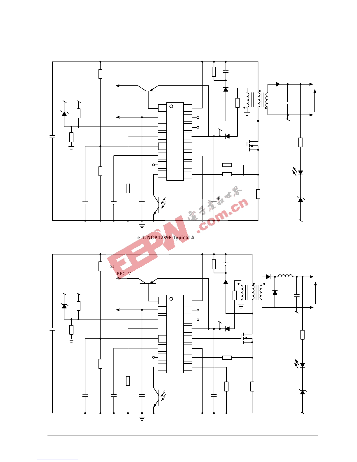
Figure 1. NCP1239F Typical Application Example
Cbulk
Vbulk
+
to PFC_V
CC
BO
1 16
2
3
4
15
14
13
NCP1239F
OVP
+
GND
V
out
Rbo1
GND
Rcomp
Cbo
5 12
6
7
8
11
10
9
Rramp
V
CC
REF5V
+
REF5V (5V/10mA)
Css
Rbo2
Rt
NTC
Thermistor
Figure 2. NCP1239V Typical Application Example
Cbulk
Vbulk
+
to PFC_V
CC
BO
1 16
2
3
4
15
14
13
NCP1239V
OVP
V
out
Rbo1
GND
Rdmax
Cbo
5 12
6
7
8
11
10
9
Rramp
V
CC
REF5V
+
REF5V (5V/10mA)
Css
Rbo2
Rt
NTC
Thermistor
D3
D4
+
GND
L2
Page 3
NCP1239
http://onsemi.com
3
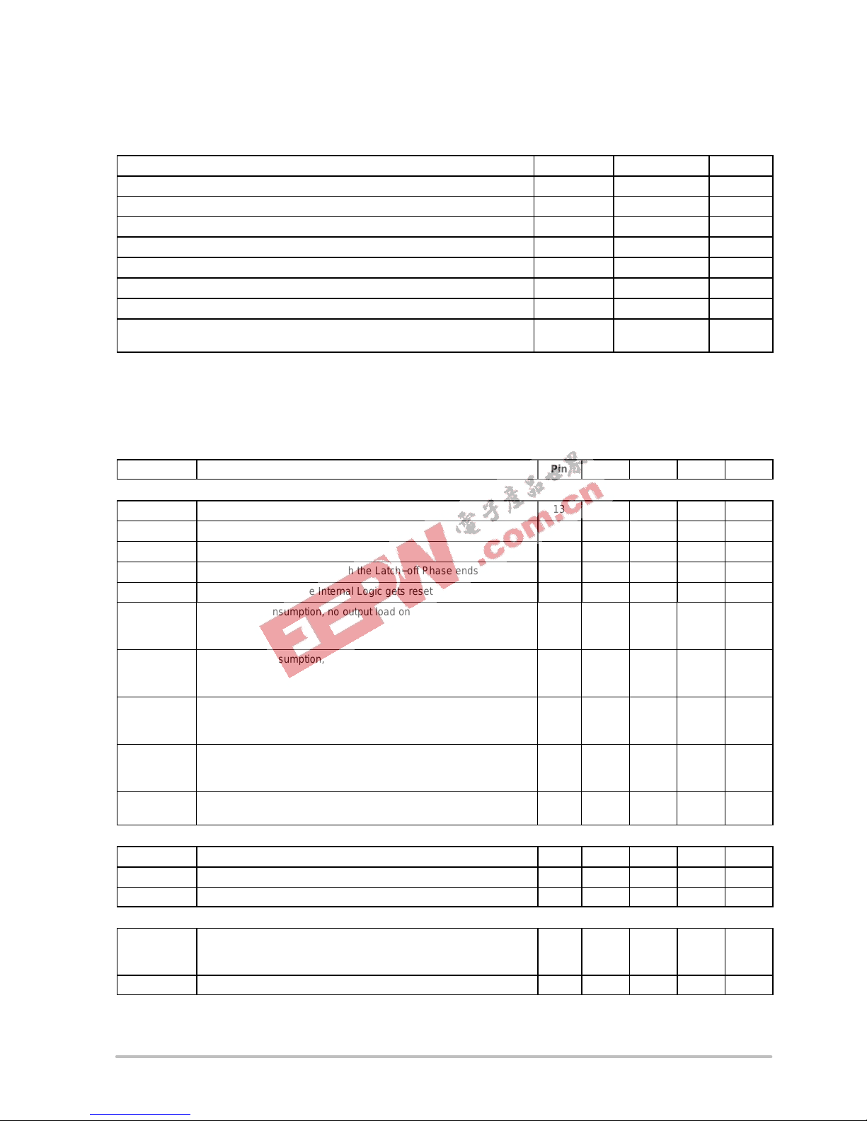
MAXIMUM RATINGS
Rating Symbol Value Unit
Power Supply Voltage V
CC
36 V
Pins 1 to 10 (except Vref Pin) Maximum Voltage −0.3, +10 V
Maximum Voltage on Pin 16 (HV) 500 V
Thermal Resistance, Junction−to−Air, SOIC Version
R
JA
145 °C/W
Maximum Junction Temperature TJ
MAX
150 °C
Storage Temperature Range −60 to +150 °C
ESD Capability, HBM Model (All Pins except HV) 2 kV
ESD Capability Machine Model (All Pins except VCC)
Machine Model (VCC Pin)
200
160
V
Maximum ratings are those values beyond which device damage can occur. Maximum ratings applied to the device are individual stress limit
values (not normal operating conditions) and are not valid simultaneously. If these limits are exceeded, device functional operation is not implied,
damage may occur and reliability may be affected.
ELECTRICAL CHARACTERISTICS (For typical values T
J
= 25°C, for min/max values TJ = 0°C to +125°C, V
pin16
= 48 V,
VCC = 20 V unless otherwise noted.)
Symbol Rating Pin Min Typ Max Unit
Supply Section
V
CCON
Turn−on Threshold Level, VCC Going up 13 15.5 16.4 17.5 V
V
CCOFF
Minimum Operating Voltage after Turn−on 13 10.5 11.2 12.2 V
HYST1 Difference (V
CCON
− V
CCOFF
) 13 4.5 5.1 − V
V
CCLATCH
VCC Decreasing Level at which the Latch−off Phase ends 13 6.5 6.9 7.2 V
V
CCRESET
VCC Level at which the Internal Logic gets reset 13 − 4.0 − V
I
CC1
Internal IC Consumption, no output load on Pin 12 (@I
Rt
= 20 A)
NCP1239F
NCP1239V
13
−
−
2.1
2.6
3.0
4.0
mA
I
CC2a
Internal IC Consumption, 1 nF output load on Pin 12
NCP1239F (65 kHz)
NCP1239V (118 kHz)
13
−
−
3.1
4.2
3.8
6.5
mA
I
CC2b
Internal IC Consumption, 1 nF output load on Pin 12
NCP1239F (100 kHz)
NCP1239V (182 kHz)
13
−
−
3.9
5.5
5.0
8.5
mA
I
CC2c
Internal IC Consumption, 1 nF output load on Pin 12
NCP1239F (130 kHz)
NCP1239V (236 kHz)
13
−
−
4.6
6.7
5.9
9.6
mA
I
CC3
Internal IC Consumption, latchoff phase
(NCP1239F and NCP1239V)
13 −
0.40 0.75
mA
Internal Startup Current Source
I
C1_hv
High−Voltage Current Source (sunk by Pin 16), VCC = 10 V 16 2.0 4.0 5.3 mA
I
C1_VCC
Startup Charge Current flowing out of the VCC Pin, VCC=10 V 13 1.8 3.6 4.5 mA
I
C2
High−Voltage Current Source, VCC = 0 16 − 4.2 − mA
5 V Reference Voltage (REF5V)
REF5V Reference Voltage
@ No load on Pin 2
@ I
pin2
= 5 mA
2
4.7
4.6
5.0
4.9
5.2
5.1
V
Iref Current Capability 2 5.0 10 − mA
Page 4
NCP1239
http://onsemi.com
4
ELECTRICAL CHARACTERISTICS (For typical values T
J
= 25°C, for min/max values TJ = 0°C to +125°C, V
pin16
= 48 V,
VCC = 20 V unless otherwise noted.)
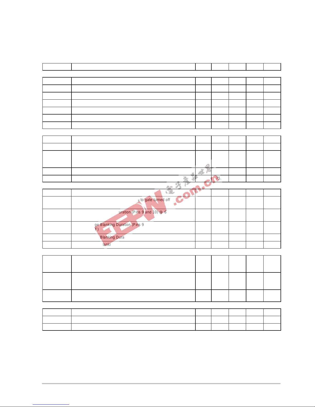
Symbol UnitMaxTypMinPinRating
Drive Output
Vcl Output Voltage Positive Clamp 12 11.5 13.6 16 V
T
rise
Output Voltage Rise−Time @ CL = 1 nF, 10−90% of output signal 12 − 40 − ns
T
fall
Output Voltage Fall−Time @ CL = 1 nF, 10−90% of output signal 12 − 25 − ns
V
source
High State Voltage Drop @ I
pin12
= 3 mA and VCC = 12 V 12 − 2.5 3.3 V
I
source
Source Current Capability (@ V
pin12
= 0 V) 12 − 500 − mA
R
OL
Sink Resistance @ V
pin12
=1 V 12 − 3.8 7.5
I
sink
Sink Current Capability (@ V
pin12
= 10 V) 12 − 800 − mA
Oscillator
fsw Recommended Switching Frequency Range 12 25 − 250 kHz
Vosc
Pin 4 Voltage @ Rt = 100 k
4 − 1.6 − V
Kosc Product (Switching Frequency times the Rt Pin 4 resistance) (Note 1)
@ 65 kHz and 130 kHz (NCP1239F)
@ 118 kHz and 236 kHz (NCP1239V)
6050
11000
6500
11800
6950
12600
kHz*k
fsw
Internal Modulation Swing, in percentage of fsw − ±3.5 − %
Dmax Maximum Duty−Cycle 75.5 80.0 83.0 %
Current Limitation
I
Limit
Maximum Internal Set−Point 10 0.84 0.90 0.95 V
T
DEL_CS
Propagation Delay from V
pin10
> I
Limit
to gate turned off
(Pin 12 loaded by 1 nF)
10 − 130 220 ns
T
LEB−65kHz
Leading Edge Blanking Duration (Pins 9 and 10) @ 65 kHz
(NCP1239F)
9, 10 − 420 − ns
T
LEB−130kHz
Leading Edge Blanking Duration (Pins 9 and 10) @ 130 kHz
(NCP1239F)
9, 10 − 230 − ns
T
LEB−118kHz
Leading Edge Blanking Duration (Pin 10) @ 118 kHz (NCP1239V) 10 − 320 − ns
T
LEB−236kHz
Leading Edge Blanking Duration (Pin 10) @ 236 kHz (NCP1239V) 10 − 170 − ns
Over Power Limit (NCP1239F)
I
ocp
Internal Current Source of the Over Power Limit Pin
@ 1 V on Pin 5 and V
pin9
= 0.5 V
@ 2 V on Pin 5 and V
pin9
= 0.5 V
9
60
120
80
160
100
185
A
V
opl
Over Power Limitation Threshold
@ TJ = 25°C
@ TJ = 0°C to 125°C
9
0.48
0.47
0.50
0.50
0.52
0.52
V
T
DEL_OCP
Propagation Delay from V
pin9
> V
opl
to gate turned off
(Pin 12 loaded by 1 nF)
9 − 130 220 ns
Maximum Duty−Cycle (Dmax) Control (NCP1239V)
I
Dmax
Pin 9 Current Source @ V
pin9
= 1.0 V and V
pin9
= 2.0 V 9 46 55 63
A
D
max
Maximum Duty Cycle @ 118 kHz and V
pin9
= 1.0 V 9 20 24 29 %
K
Dmax
Dmax Coefficient @ 118 kHz and V
pin9
= 1.0 V (Note 2) 9 1.10 1.30 1.53
%/k
1. The nominal switching frequency fsw equals: fsw = K
OSC
/Rt. The implemented jittering makes the switching frequency continuously vary
around this nominal value ($3.5% variation).
2. K
Dmax
is the proportionality coefficient that links the maximum duty−cycle to the Pin 9 resistor: Dmax = K
Dmax*Rpin9
. K
Dmax
is defined in
the “Maximum Duty−Cycle Limitation” section of the operating description.
Page 5

NCP1239
http://onsemi.com
5
ELECTRICAL CHARACTERISTICS (For typical values T
J
= 25°C, for min/max values TJ = 0°C to +125°C, V
pin16
= 48 V,
VCC = 20 V unless otherwise noted.)
Symbol UnitMaxTypMinPinRating
Soft−Start and Timer
I
ch
Soft−Start or Jittering charge current @ V
pin6
= 2.4 V 6 60 95 110
A
I
disch
Jittering Discharge Current @ V
pin6
= 2.4 V 6 77 107 137
A
V
jitter
Jittering Saw−Tooth Lower Threshold 6 1.67 1.80 1.89 V
V
jitter
H Jittering Saw−Tooth Upper Threshold 6 2.85 3.00 3.20 V
V
timer
L Timer Peak Threshold 6 4.0 4.3 4.6 V
I
timerC
Timer Charge Current @ V
pin6
= 3.5 V and Pin 8 open 6 3.9 5.2 6.4
A
I
timerD
Timer Discharge Current @ V
pin6
= 3.5 V and Pin 8 open 6 − 400 −
A
Feedback Section
Rup Internal Pullup Resistor 8 − 20 −
k
Ifb Source Current @ V
pin8
= 0.5 V 8 − 200 −
A
Iratio Pin 8 to current Setpoint division ratio − − 3.0 − −
Internal Ramp Compensation
R
ramp
Internal Resistor 10 − 32 −
k
V
ramp
Internal Saw−Tooth Amplitude 10 − 3.2 − V
Skipping Mode and Standby Management
Rgts Pin 1 output impedance in standby state
(Pin 8 grounded, V
pin6
> 4.5 V) @ VCC = 12.5 V
1 4.0 8.0 18
k
Igts Sink Current Source in Normal Mode
@ V
pin8
= 2 V, Pin 7 open @ V
CC
− V
pin1
=0.7 V
1 0.6 1.0 − mA
FB−skip Default Feedback Level for Skip−Cycle Operation and Standby
Detection
7 380 430 480 mV
FB_stby−out Default Feedback Level to Leave Standby 7 650 740 810 mV
V
stby−out/Vskip
Ratio leave standby Setpoint to skip−cycle Setpoint 1.5 1.7 1.9 −
R
pin7
Internal Pin 7 Impedance 7 − 110 −
k
Pin 7 to Skipping Setpoint ratio − 3.0 − −
Brown−Out Detection
BO
thH
Brown−Out Detection Upper Threshold 5 0.45 0.50 0.55 V
BO
thL
Brown−Out Detection Low Threshold 5 0.20 0.24 0.28 V
BO
hyst
Brown−Out Hysteresis 5 0.20 0.26 0.30 V
Protections
TSD Thermal Shutdown:
Thermal Shutdown Threshold
Hysteresis
140
30
°C
Vfault Fault Detection Threshold 3 2.2 2.4 2.6 V
ORDERING INFORMATION
Device Package Shipping
†
NCP1239FDR2 SOIC−16 2500 / Tape & Reel
NCP1239FDR2G SOIC−16
(Pb−Free)
2500 / Tape & Reel
NCP1239VDR2 SOIC−16 2500 / Tape & Reel
NCP1239VDR2G SOIC−16
(Pb−Free)
2500 / Tape & Reel
†For information on tape and reel specifications, including part orientation and tape sizes, please refer to our Tape and Reel Packaging
Specifications Brochure, BRD8011/D.
Page 6

NCP1239
http://onsemi.com
6
PIN FUNCTION DESCRIPTION
Pin No. Pin Name Function Pin Description
1 GTS Shuts the PFC down in
standby
The standby detection block changes Pin 1 state in accordance to the mode
(standby or normal mode). Pin1 is designed to drive an external pnp transistor that
connects or disconnects the NCP1239’s VCC to the PFC’s.
2 REF5V A 5V reference voltage This pin helps to internally bias the controller but can also be used to power
surrounding logic gates for any purposes. The typical output current is 10 mA. This
voltage source is disabled during the circuit startup and latched−off phases. A
100 nF filtering capacitor must be placed between Pin 2 and ground.
3 Fault Detect Enables to permanently
shutdown the part
If the Pin 3 voltage exceeds 2.4 V, the circuit is permanently shut down. This pin
can be used to monitor the voltage across a thermistor in order to protect the
application from excessive heating and/or to detect an overvoltage condition.
4 Rt Timing resistor Pin 4 resistor allows a precise frequency programming. The circuit is optimized to
operate between 50 kHz and 150 kHz (NCP1239F) and between 100 kHz and
250 kHz (NCP1239V).
5 Brown−Out Brown−Out This pin receives a portion of the bulk capacitor to authorize operation above a
certain level of mains only. It also serves to elaborate an offset voltage on Pin 9
used for Over Power Compensation.
6 SS/Timer Performs soft−start and
fault timeout
During Power on and fault conditions, the capacitor connected to this pin ensures a
soft−start period. When a fault is detected, this pin is internally brought high by a
current source. If 4.3 V are reached, the fault is confirmed and the circuit enters an
auto−recovery burst mode, otherwise the pin goes back to a lower value and
oscillates to perform frequency jittering.
7 Skip Adjust Adjust skip level By adjusting the skip−cycle level, it is possible to fight against noisy transformers
and modify the standby detection thresholds. Keep Pin 7 open to operate with the
default levels (skip threshold setpoint: 140 mV, normal mode recovery setpoint:
250 mV).
8 FB Feedback signal An opto−coupler collector pulls this pin low to regulate
9 Over Power
Limit
(NCP1239F)
Enables a precise peak
current clamp and then an
accurate Over Power
Detection
This pin delivers a current proportional to V
pin5
, an image of the high voltage rail.
Inserting a resistor between Pin 9 and the current sense resistor, an offset
proportional to the input voltage is built. Such offset compensates the circuit and
power switch propagation delays for an accurate power limitation in the whole input
voltage range.
9 Max Duty−
Cycle
(NCP1239V)
Enables to precisely
clamp the maximum
duty−cycle.
This terminal sources a constant current. Connect a resistor between Pin 9 and
Ground to select the maximum duty−cycle.
10 CS The current sense input This pin receives the primary current information via a sense element. By inserting
a resistor in series with this pin, it becomes possible to introduce ramp
compensation.
11 Ground The IC ground −
12 Drv Drives the MOSFET By offering up to +500 mA/−800 mA peak, this pin lets you drive large Qg
MOSFET’s. It is clamped to 16 V maximum not to exceed the maximum
gate−source voltage of most power MOSFET’s.
13 V
CC
Supplies the controller This pin accepts up to 36 V from an auxiliary winding.
14 NC − Creepage distance.
15 NC − Creepage distance.
16 HV The high−voltage startup This pin connects to the bulk capacitor to generate the startup current.
Page 7
NCP1239
http://onsemi.com
7
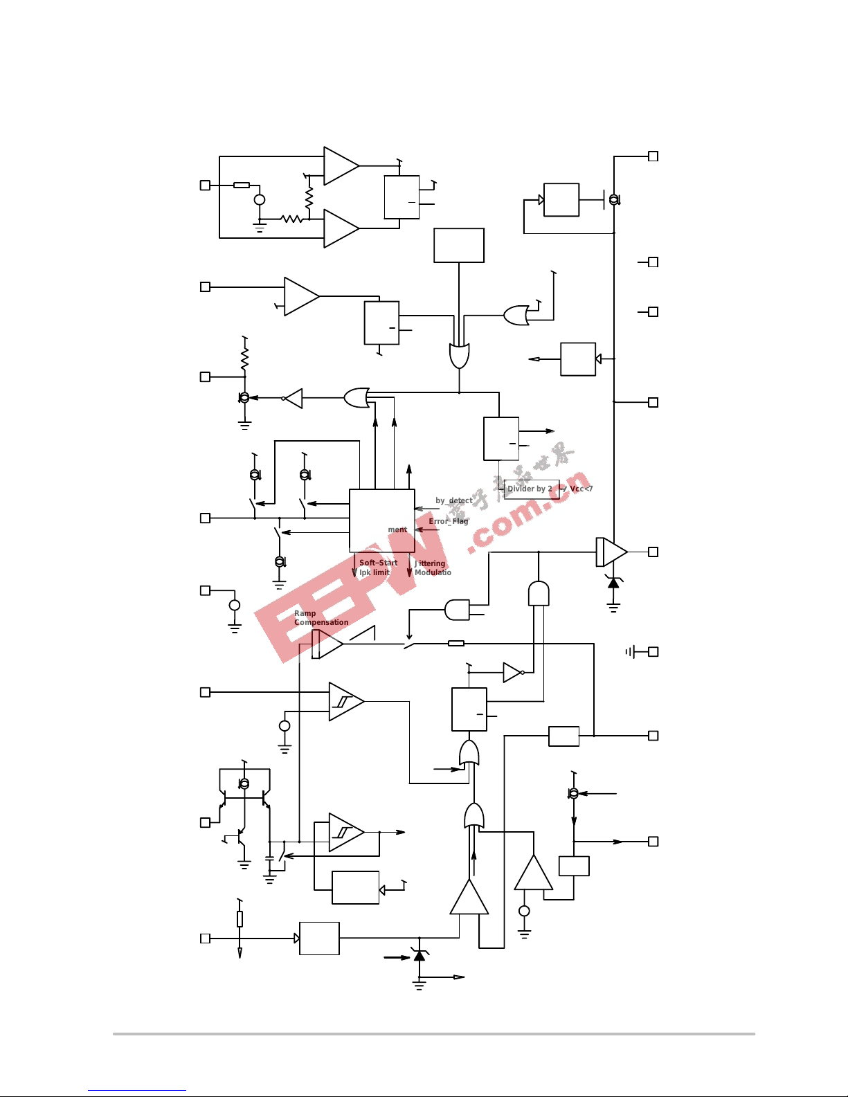
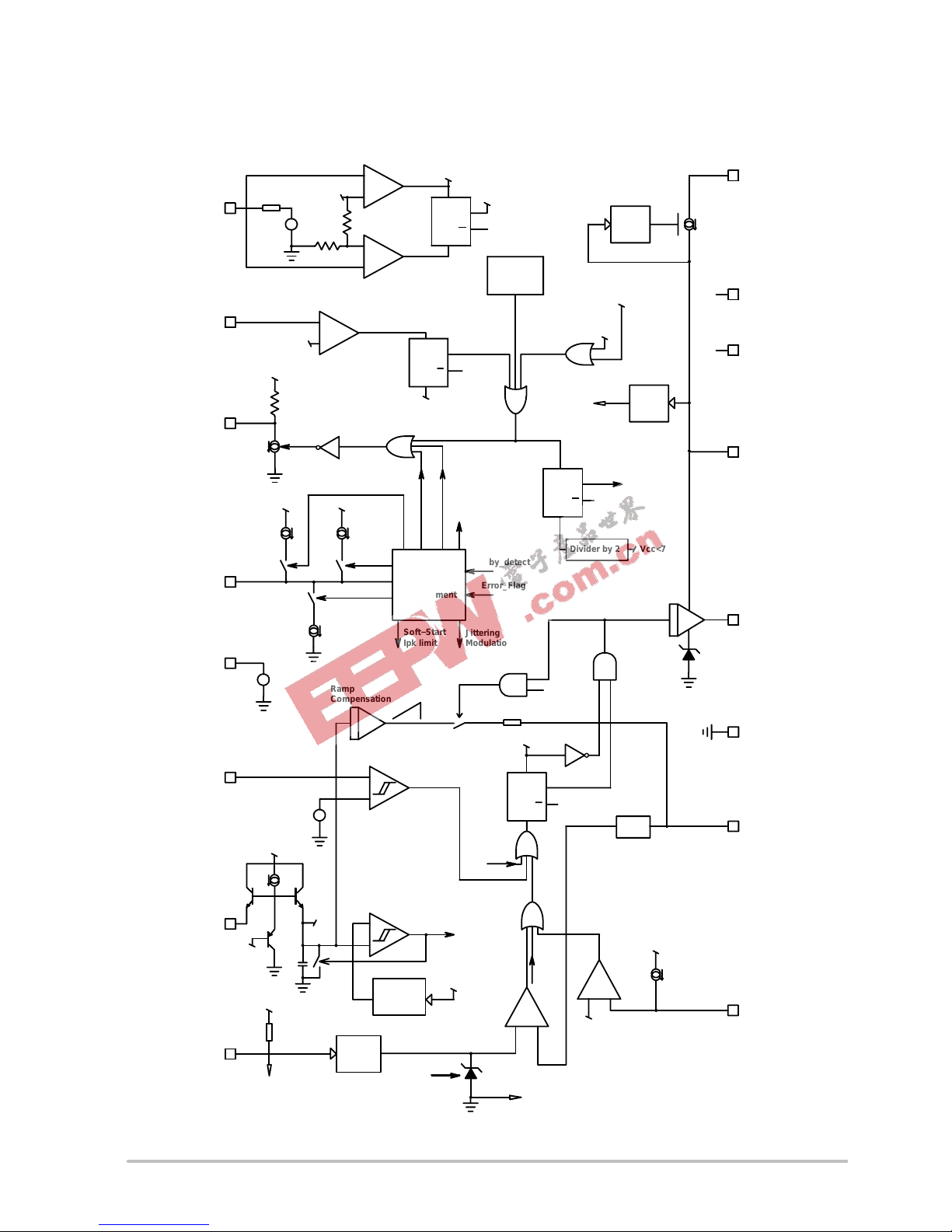
Figure 3. NCP1239F Internal Circuit Architecture
−
+
7
S
R
Q
Q
Vcc < 4V
450mV
5V
0.5V / 0.25V
Rt
BO
REF5V
SS / timer
PFC_Vcc
Fault
detect
Skip
adjust
Vdd
/ 3
to Skip
20k
0.9V
Oscillator
GND
32k
CS
Drv
Vcc
Vdd
Regul
UVLOs
Latch
Reset
Error flag
HV
Over Power
Limit
Vdd
2.5V
Vdd
2.5V
100k
Fault
Vdd Vdd
Soft−Start
and timer
management
Stby_detect
Error_Flag
Stby
OVL
OVL
Vcc<7V
stdwn
Vstop
PWM Latch
Output
Buffer
BO_out
Jittering
Modulation
“Jittered”
Reference
Jittering
Modulation
CLK
CLK
0.5V
BO_in
Soft−Start
Ipk limit
Soft−Start
Ipk limit
Internal
Thermal
Shutdown
TSD
FB
Divider by 2
+
−
Skip
Skip
FB
Startup Phase
(Vcc<VccOFF)
1mA
Vcc
10k
Vstop
regOUT
Stby_detect
25r
15r
S
R
Q
Q
FB<Vpin1 => Skip high
FB>1.6*Vpin1 =>Stby_detect RESET
pfcOFF
pfcON
UVLO
14V
clamp
pfcON
OUTon
Ramp
Compensation
3.2V
BO_in
75 mA/V x V
pin5
LEB
LEB
+
−
+
16
15
14
13
−
+
3
1
S
R
Q
Q
6
2
+
12
11
10
5
+
S
R
Q
Q
9
+
−
+
−
+
−
+
8
4
Page 8
NCP1239
http://onsemi.com
8
Figure 4. NCP1239V Internal Circuit Architecture
−
+
7
S
R
Q
Q
Vcc < 4V
450mV
5V
0.5V / 0.25V
Rt
BO
REF5V
SS / timer
PFC_Vcc
Fault
detect
Skip
adjust
Vdd
/ 3
to Skip
20k
0.9V
Oscillator
GND
32k
CS
Drv
Vcc
Vdd
Regul
UVLOs
Latch
Reset
Error flag
HV
Dmax
Vdd
2.5V
Vdd
2.5V
100k
Fault
Vdd Vdd
Soft−Start
and timer
management
Stby_detect
Error_Flag
Stby
OVL
OVL
Vcc<7V
stdwn
Vstop
PWM Latch
Output
Buffer
BO_out
Jittering
Modulation
“Jittered”
Reference
Jittering
Modulation
CLK
CLK
BO_in
Soft−Start
Ipk limit
Soft−Start
Ipk limit
Internal
Thermal
Shutdown
TSD
FB
Divider by 2
+
−
Skip
Skip
FB
Startup Phase
(Vcc<VccOFF)
1mA
Vcc
10k
Vstop
regOUT
Stby_detect
25r
15r
S
R
Q
Q
FB<Vpin1 => Skip high
FB>1.6*Vpin1 =>Stby_detect RESET
pfcOFF
pfcON
UVLO
14V
clamp
pfcON
OUTon
Ramp
Compensation
3.2V
Idmax
LEB
+
−
+
16
15
14
13
−
+
3
1
S
R
Q
Q
6
2
+
12
11
10
5
+
S
R
Q
Q
9
+
−
−
+
−
+
8
4
OSC
OSC
Page 9

NCP1239
http://onsemi.com
9
Figure 5. High Voltage Current Source
vs. Temperature @ V
CC
= 10 V
Figure 6. Startup Current Sourced by V
CC
Pin
vs. Temperature @ V
CC
= 10 V
TEMPERATURE (°C)
100755025−25
I
C1_VCC
(mA)
TEMPERATURE (°C)
125100755025
6.0
I
C1_HV
, (mA)
5.0
−25
0
4.0
3.0
2.0
1.0
0
5.0
4.5
4.0
3.5
3.0
2.5
2.0
1.5
1.0
0.5
0
TYPICAL PERFORMANCE CHARACTERISTICS
Figure 7. High Voltage Current Source
vs. Temperature @ V
CC
= 0 V
TEMPERATURE (°C)
125100755025−25
I
C2
(mA)
6.0
0
5.0
4.0
3.0
2.0
1.0
0
Figure 8. High Voltage Pin Leakage Current
vs. Temperature
12
5
TEMPERATURE (°C)
12
5
100755025
0
10
20
30
Pin16 Leakage Current (A)
40
50
60
0
Figure 9. VCC Startup Threshold
vs. Temperature
TEMPERATURE (°C)
125100755025
V
CCON
(V)
16.7
0
16.6
16.5
16.4
16.3
16.2
16.1
16.0
15.9
Figure 10. VCC Turn−Off Threshold
vs. Temperature
11.5
TEMPERATURE (°C)
1
25
100755025−25
V
CCOFF
(V)
0
11.4
11.3
11.2
11.1
11.0
10.9
10.8
0
Page 10
NCP1239
http://onsemi.com
10
TEMPERATURE (°C)
125100755025−25
6.75
6.80
6.85
6.90
V
CCLATCH
(V)
6.95
0
TYPICAL PERFORMANCE CHARACTERISTICS
Figure 11. VCC Latched−Off vs. Temperature
TEMPERATURE (°C)
12
5
100755025−25
1.6
2.2
2.8
I
CC1
(mA)
Figure 12. No Load Circuit Consumption
vs. Temperature
1.8
2.0
2.4
2.6
0
TEMPERATURE (°C)
125100755025−25
2.0
2.5
3.0
3.5
4.0
I
CC2
(mA)
Figure 13. NCP1239F Circuit Consumption
(1 nF on driver Pin 12) vs. Temperature
130 kHz
4.5
5.0
100 kHz
65 kHz
0
TEMPERATURE (°C)
12
5
100755025−25
I
CC2
(mA)
Figure 14. NCP1239V Circuit Consumption
(1 nF on driver Pin 12) vs. Temperature
7.3
200 kHz
130 kHz
0
6.9
6.5
6.1
5.7
5.3
4.9
4.5
4.1
3.7
3.3
260 kHz
TEMPERATURE (°C)
125100755025−25
I
CC3
(mA)
Figure 15. Latched−Off Mode Consumption
vs. Temperature
4.70
4.85
4.90
4.95
TEMPERATURE (°C)
12
5
100755025−25
REF5V (V)
4.80
0 mA
5 mA
10 mA
0.6
5.00
5.05
0
4.75
0
0.5
0.4
0.3
0.2
0.1
0
Figure 16. REF5V Voltage Source
vs. Temperature
Page 11

NCP1239
http://onsemi.com
11
TEMPERATURE (°C)
125100755025−25
2.0
3.0
8.0
Vdrop (V)
TEMPERATURE (°C)
12
5
100755025−25
Rsink ()
0
5.0
6.0
4.0
TYPICAL PERFORMANCE CHARACTERISTICS
Figure 17. Driver High State Voltage Drop
vs. Temperature
Figure 18. Driver Sink Resistance
vs. Temperature
3.0
00
12300
TEMPERATURE (°C)
TEMPERATURE (°C)
12
5
100755025−25
79
81
83
125100755025−25
6700
Dmax (%)
K
osc
(kHz*k)
130 kHz
77
78
80
82
Figure 19. Driver Voltage Clamp vs. Temperature Figure 20. Maximum Duty Cycle vs. Temperatur
e
(NCP1239F)
Figure 21. Oscillator K
osc
Parameter vs. Temperature
(K
osc
= fsw * R
pin4
) (NCP1239F)
TEMPERATURE (°C)
125100755025−25
16
Vcl CLAMP VOLTAGE (V)
65 kHz
0 0
0
TEMPERATURE (°C)
12
5
100755025
K
osc
(kHz*k)
K
osc1
@ 130 kHz
Figure 22. Oscillator K
osc
Parameter vs. Temperature
(K
osc
= fsw * R
pin4
) (NCP1239V)
K
osc2
@ 260 kHz
−25
2.9
2.8
2.7
2.6
2.5
2.4
2.3
2.2
2.1
2.0
7.0
1.0
15
14
13
12
10
11
10
6650
6600
6550
6500
6450
6400
12150
12000
11850
11700
11550
11400
11250
0
Page 12

NCP1239
http://onsemi.com
12
TEMPERATURE (°C)
12
5
100755025−25
410
415
420
430
435
FB
skip
(mV)
425
445
450
440
0
125
40
60
80
120
140
180
TEMPERATURE (°C)
100755025−25
I
ocp
(
A)
100
160
BO = 2 V
BO = 1 V
0
TYPICAL PERFORMANCE CHARACTERISTICS
TEMPERATURE (°C)
1
25
100755025−25
0.508
V
opl
(V)
Figure 23. Pin 9 Current vs. Temperature
(@ V
pin9
= 0.5 V) (NCP1239F)
Figure 24. Over Power Limitation Threshold vs
.
Temperature (NCP1239F)
0
0.506
0.504
0.502
0.500
0.498
0.496
0.494
0.492
TEMPERATURE (°C)
12
5
100755025−25
BO_H (V)
0.510
TEMPERATURE (°C)
125100755025−25
FB
stby−out
(mV)
780
0
0
TEMPERATURE (°C)
125100755025−25
0.920
I
Limit
(V)
0
Figure 25. Maximum Current Setpoint vs.
Temperature
Figure 26. Default Feedback Threshold for
Standby Detection vs. Temperature
Figure 27. Default Feedback Level for Normal
Operation Recovery
Figure 28. Brown−Out Upper Threshold vs.
Temperature
0.915
0.910
0.905
0.900
0.895
0.890
0.890
0.885
0.880
770
760
750
740
730
720
710
700
0.505
0.500
0.495
0.490
0.485
0.480
Page 13

NCP1239
http://onsemi.com
13
TYPICAL PERFORMANCE CHARACTERISTICS
TEMPERATURE (°C)
125100755025−25
0.245
BO_L (V)
0
TEMPERATURE (°C)
12
5
100755025−25
2.51
V
fault
(V)
0
Figure 29. Brown−Out Low Threshold vs.
Temperature
Figure 30. Fault Detect Threshold vs. Temperature
TEMPERATURE (°C)
125100755025
Dmax (%)
24.5
0
Figure 31. Maximum Duty−Cycle vs.
Temperature @ V
pin9
= 1 V (NCP1239V)
Figure 32. Kdmax Coefficient vs.
Temperature @ V
pin9
= 1 V (NCP1239V)
TEMPERATURE (°C)
12
5
100755025
1.35
Kdmax (%/k)
0
1.33
1.31
1.29
1.27
1.26
0.244
0.243
0.242
0.241
0.240
0.239
0.238
0.237
0.236
0.235
2.49
2.47
2.45
2.43
2.41
2.39
2.37
2.35
24.3
24.1
23.9
23.7
23.5
Page 14

NCP1239
http://onsemi.com
14
Figure 33. Fault Management
10ms* Jittering
100ms*
fmax
fmin
0.9 V
Error flag
16.4V
11.2V
Fb is ok
Fault occurs here
6.9V
OVL signal
(Over−Load)
DRV
Vcc
Reset at UVLO
Fault not confirmed
PFC off
PFC on
1.8V
3.0V
4.3V
PFC off
100ms*
Fault confirmed
New Startup
attempt
SS / timer pin
0.9 V
Error flag
0.9 V
Error flag
Fault Management
*This time is programmed by the Pin 6 capacitor. C
pin6
= 390 nF nearly sets the following intervals:
− Soft−Start Time (Tss):7.5 ms
− Jittering Period (T
jittering
): 10 ms
− Fault Detection Delay (T
delay
): 100 ms
More generally, the times approximately depend on C
pin6
as follows:
−Tss = 7.5 ms * C
pin6
/ 390 nF
−T
jittering
=10 ms * C
pin6
/ 390 nF
−T
delay
=100 ms * C
pin6
/ 390 nF
Page 15

NCP1239
http://onsemi.com
15
Figure 34. Standby Detection
Jittering 10ms*
Vpin6
(SS/timer)
Fb is ok
Drv
FB
PFC running
Standby is entered Standby is left
PFC is down
Skip activity
Standby is not confirmed
Standby is confirmed,
No delay
Stby_detect latch is armed
Stby_detect latch is reset
100ms*
100ms*
delay
FB−skip (Vpin7)
FB−stby−out (1.7*Vpin7)
4.3V
3.0V
1.8V
Bunches of pulses
Standby Detection
*This time is programmed by the Pin 6 capacitor. C
pin6
= 390 nF nearly sets the following intervals:
− Soft−Start Time (Tss):7.5 ms
− Jittering Period (T
jittering
): 10 ms
− Fault Detection Delay (T
delay
): 100 ms
More generally, the times approximately depend on C
pin6
as follows:
−Tss = 7.5 ms * C
pin6
/ 390 nF
−T
jittering
=10 ms * C
pin6
/ 390 nF
−T
delay
=100 ms * C
pin6
/ 390 nF
Page 16

NCP1239
http://onsemi.com
16
APPLICATION INFORMATION
The NCP1239 includes all necessary features to help
building a rugged and safe switch−mode power supply. The
following details the major benefits brought by
implementing the NCP1239 controller:
Current−mode operation with internal ramp
compensation: implementing peak current mode control,
the NCP1239 offers an internal ramp compensation signal
that can easily be summed up to the sensed current.
Subharmonic oscillations can thus be fought via the
inclusion of a simple resistor,
500 mV Current Sense threshold for Over Power Limit
(NCP1239F): the NCP1239 operating in current mode, the
circuit Pin 10 monitors the current to modulate its level
according to the power demand. Due to the ramp
compensation, one must generally note that the Pin 10
voltage is not the exact image of the inductor current. A
precise current limitation being essential, the NCP1239
features a separate current sense pin (Pin 9) for an accurate
overcurrent detection. The low threshold of this protection
(500 mV) avoids excessive losses in the current sense
resistor and improves the efficiency. In addition, Pin 9
sources a current that proportional to the high−voltage rail,
compensates the current−sense and turn off delays at high
line. A resistor inserted between Pin 9 and the sensing
resistor offsets the Pin 9 current−sense information to build
a precise overload protection, independent of the mains
input.
Large VCC operation: the NCP1239 offers an extended
VCC range up to 36 V, bringing greater flexibility in Flyback
or Forward applications.
Internal high−voltage startup switch: reaching low
levels of standby power represents a difficult exercise when
the controller requires an external, lossy, resistor connected
to the bulk capacitor. Due to an internal logic, the controller
disables the high−voltage current source after startup which
no longer hampers the consumption in no−load situations.
Skip−cycle capability: a continuous flow of pulses is not
compatible with no−load standby power requirements.
Slicing the switching pattern in bunch of pulses drastically
reduces overall losses but can, in certain cases, bring
acoustic noise in the transformer. Due to a skip operation
taking place at low peak currents only, no mechanical noise
appears in the transformer. Furthermore, the skip threshold
is made programmable to allow the best trade−off between
noise and efficiency.
Standby Detect/Shutdown of the PFC front−stage: The
NCP1239 incorporates an internal logic that is able to detect
a standby situation. Pin1 state changes in accordance to the
detected mode (standby or normal mode). Simply connect a
pnp transistor between the NCP1239 VCC and the PFC
controller one and drive it using Pin 1, to enable the PFC
stage in normal mode and disable it in standby.
Soft−Start: the capacitor connected to Pin 6 provides a
soft−start sequence that precludes the main power switch
from being stressed upon startup. The same voltage is also
used to perform frequency jittering and timing for the fault
condition detection.
Major Fault Detection: the circuit detects when Pin 3
voltage exceeds 2.4 V. When this occurs, the NCP1239
considers that a major fault is present and as a consequence,
the circuit gets permanently latched−off. In this mode, the
circuit needs the VCC to go down below 4.0 V to reset, for
instance when the user un−plugs the SMPS. This capability
is mainly intended to detect an overvoltage condition or/and
an over−heating of the application that would be sensed by
a thermistor.
Brown−out detection: by monitoring the level on Pin 5
during normal operation, the controller protects the SMPS
against low mains conditions. When the Pin 5 voltage falls
below 250 mV, the controllers stops pulsing until this level
goes back to 500 mV to prevent any instability.
Short−circuit protection: short−circuit and especially
overload protections are difficult to implement when a
strong leakage inductance affects the transformer (the
auxiliary winding level does not properly collapse…). Here,
every time the feedback pin is at its maximum (higher than
5.0 V practically), an error flag is asserted and the circuit
activates a timer that is programmed by the Pin 6 capacitor.
If Pin 6 reaches 4.3 V while the error flag is still present, the
controller stops the pulses and goes into a latch−off phase,
operating in a low−frequency burst−mode. As soon as the
fault disappears, the SMPS resumes its operation. The
latch−off phase can also be initiated, more classically, when
VCC drops below UVLO (11.2 V typical).
Adjustable frequency and Internal dithering for
improved EMI signature: Pin 4 offers a means to precisely
adjust the switching frequency through a simple resistor to
ground. Frequency operation is allowed up to 250 kHz. By
modulating the internal switching frequency with the Pin 6
saw−tooth (100 Hz with 390 nF), natural energy spread
appears and softens the controller’s EMI signature.
5.0 V reference voltage: a 5.0 V regulator is provided to
help biasing any external circuitry in the vicinity of the
controller. This reference voltage can typically supply up to
10 mA.
Page 17

NCP1239
http://onsemi.com
17
Startup Sequence
When the power supply is first connected to the mains
outlet, the internal current source (typically 3.6 mA) is
biased and charges up the VCC capacitor. When the voltage
on this VCC capacitor reaches the V
CCON
level (typically
16.4 V), the current source turns off and no longer wastes
any power. At this time, the energy stored by the V
CC
capacitor serves to supply the controller and the auxiliary
supply is supposed to take over before VCC collapses below
V
CCOFF
. Figure 35 shows the internal arrangement of this
structure:
Figure 35.
The current source brings V
CC
above 16.4 V and then turns o
ff
16
13
10
3.6 mA/0
CV
CC
Aux
HV
16.4 V /
11.2 V
−
+
As soon as VCC reaches 16.4 V, driving pulses are
delivered on Pin 12 and the auxiliary winding grows up the
VCC pin. Because the output voltage is below the target (the
SMPS is starting up), the feedback pin is at its maximum
voltage. A resistor divider outputs the third of the feedback
voltage that forms the current setpoint. This setpoint is
clamped and the limitation level slowly increases until it
reaches 0.9V during the soft start time. In nominal operation,
the setpoint clamp keeps equal to 0.9 V (refer to Figure 36).
As soon as the feedback voltage is high enough to activate
the 0.9 V setpoint clamp (during the startup period but also
anytime an overload occurs), an internal error flag is
asserted, testifying that the system is pushed to the
maximum power. At that moment, a 100 ms time period
(typically, with C
pin6
=390 nF that also corresponds to 7.5 ms
soft −start) starts while a logic block observes this error flag.
If the error flag keeps asserted all along the 100ms period,
then the controller assumes that the power supply really
undergoes a fault condition and immediately stops all pulses
to enter a safe burst operation. The 100 ms timer enables to
distinguish a startup phase (shorter than 100 ms) from an
overload condition. If the error flag is released before the
100 ms period has elapsed, the controller concludes that no
error is present and resets the timer to use it for other
purposes (e.g. frequency dithering).
Figure 36. Current Control
Pin 10 monitors the power switch current and compares it to the current setpoint (one third of the feedback voltage). The
current setpoint is limited by the soft−start during the power−on sequence and permanently clamped to 0.9 V In the
NCP1239F, a second pin (Pin 9) monitors the current to clamp the power.
−
+
CLK
Current Sense
Comparator
8
10
Current Sense
Over Power
Comparator
Feedback
Rramp
Rsense
Vdd
0.9 V
Vin
Overcurrents Compensation
to
Standby Management
(Skipping, GTS)
S
R
Q
Q
LEB
PWM Latch
+
−
Rcomp
+
9
Over Power
Limit
500 mV
LEB
Pin 5 (Brown−Out)
/ 3
Ramp Compensation
oscillator
Soft−Start
20k
Page 18

NCP1239
http://onsemi.com
18
Figure 37 depicts the VCC evolution during a proper startup sequence, showing the state of the error flag:
*This time is programmed by the Pin 6 capacitor. C
pin6
= 390 nF nearly sets the following intervals:
− Soft−Start Time (Tss):7.5 ms
− Jittering Period (T
jittering
): 10 ms
− Fault Detection Delay (T
delay
): 100 ms
More generally, the times approximately depend on C
pin6
as follows:
−Tss = 7.5 ms * C
pin6
/ 390 nF
−T
jittering
=10 ms * C
pin6
/ 390 nF
−T
delay
=100 ms * C
pin6
/ 390 nF
Figure 37.
7.5ms*
SS
Ip max
FB
Error
Flag
Timer
Full power
Skip level
VccON
VccOFF
Vcc
Latch−off phase level
Logic reset level
regulation
No error has
been confirmed
User
Powers up!
Feedback loop
reacts...
Page 19

NCP1239
http://onsemi.com
19
PFC Startup Sequence
To ensure an adequate startup sequence of both PWM
section and the PFC stage, some logic and timing need to be
included as shown on the internal diagram. The key point
here is the fact that the PFC always starts after the PWM
section. As a result, the SMPS must be designed to cope with
transient universal mains operation. Why this? Because of
the light−to−heavy load transition where a case exists when
the PFC is off, the PWM in standby and the load is suddenly
applied. In this scenario, the PWM section must sustain the
entire transient period that lasts until the PFC re−starts since
it has been deactivated for standby.
The standby detection block generates an internal signal
“pfcON” that controls Pin 1 in accordance to the operation
mode:
− “pfcON” is high in normal mode and a current source
draws 1 mA from Pin 1,
− “pfcON” is low in standby to disable the 1 mA current
source. A 10 k resistor pulls up Pin 1 to VCC.
This configuration makes it ideal to drive a pnp transistor
that connects or disconnects the NCP1239 VCC to the PFC
controller one (refer to Figure 39). The “pfcON” signal is
activated following Figure 38 diagram. Let’s split this
drawing in different time periods to clearly depict signal
assertions:
Power on: during this time, VCC rises up, the V
CC
capacitor being charged by the 3.6 mA current source. When
VCC exceeds V
CCON
(16.4 V typ.), driving pulses are
delivered to the MOSFET in an attempt to crank the power
supply. VCC collapses (because the VCC capacitor alone
delivers the energy) until sufficient auxiliary voltage is built
up in order to take over the startup sequence and thus
self−supply the controller. As long as the output voltage has
not reached its wished value, the controller pushes for the
maximum peak current. During the soft−start (7.5 ms with
390 nF on Pin 6), the maximum permissible current linearly
increases till the maximum peak setpoint is reached, the
internal 0.9 V Zener diode actively clamping the current
amplitude to (0.9 V/Rsense). During this time, the NCP1239
asserts an error flag. A maximum current condition being
observed, the circuit determines if this state results from
either a normal response (startup or a transient period) or a
fault condition. To make the difference, each time the error
flag is asserted, a 100 ms timer starts to count down. If the
error flag keeps asserted for the 100 ms period, there is a
fault and the PWM controller enters a safe, auto−recovery,
burst mode to limit the dissipated heat (see below for more
details). During the Power−on sequence, “pfcON” keeps
low to pullup Pin 1 to VCC until the error flag is down. When
the error flag is down, the power supply has entered
regulation, its auxiliary voltage is stable, then Pin 1 can turn
low (1 mA sink current) to safely allow PFC operation.
Entering Standby: when skip−cycle starts to activate, a
100 ms countdown takes place and the logic observes the
skip activity. I f the skip activity is still there at the end of the
100 ms, then standby is confirmed and the NCP1239 pulls
up Pin 1 to VCC to shut down the PFC.
Leaving standby: in this case, as soon as the skip−cycle
activity disappears, the circuit immediately re−activates the
1 mA sinking current source of Pin 1, to enable the PFC:
there is no reaction delay in this situation.
Short−circuit condition: a short circuit is detected on the
primary side by measuring the time the error flag is asserted.
As explained, if this flag is asserted longer than 100 ms, then
the PWM stops oscillating and enters a safe burst mode. In
this case, Pin 1 is pulled up to VCC and the PFC is s hut down.
During the burst, it is not activated (PFC is off) until the fault
goes away and the power supply resumes operation. The
PFC being shut off in short−circuit conditions, it naturally
reduces the main MOSFET stress.
Latch−off mode: if the controller is permanently
latched−off due to a major fault (Pin 3 detection of an OVP
or an excessive external temperature), the PFC is kept off
(Pin 1 being tied to VCC).
Page 20

NCP1239
http://onsemi.com
20
*This time is programmed by the Pin 6 capacitor. C
pin6
= 390 nF nearly sets the following intervals:
− Soft−Start Time (Tss):7.5 ms
− Jittering Period (T
jittering
): 10 ms
− Fault Detection Delay (T
delay
): 100 ms
More generally, the times approximately depend on C
pin6
as follows:
−Tss = 7.5 ms * C
pin6
/ 390 nF
−T
jittering
=10 ms * C
pin6
/ 390 nF
−T
delay
=100 ms * C
pin6
/ 390 nF
Figure 38.
Vcc
PWM
Timer
0.9V
flag
PFC
Vcc
regulation
100ms*
16.4V
11.2V
6.9V
100ms* 100ms* 100ms*
7.5ms*
SS
Short−circuit
Stby stby is left
Standby
is confirmed
Nom
Pout
Short−circuit
One Vcc cycle is skipped to
lower the burst mode duty
cycle to typically 5% in
fault conditions.
If the fault had disappeared
the SMPS would recover
normal operation
Page 21

NCP1239
http://onsemi.com
21
The PFC controller connection is really straightforward as
testified by Figure 39: simply connect to Pin 1, the base of
a pnp transistor that connects the PFC’s VCC to the NCP1239
one (perhaps add a small decoupling capacitor like a 0.1 F
on the PFC) and this is all! The PFC startup network goes
away as it is fully supplied by the PWM auxiliary winding
and even high quiescent current devices do not hamper the
standby power since they are completely disconnected in
standby.
Figure 39.
The NCP1239 turns off the pnp Q1 during the standby so that the PFC controller is no longer supplied in this mode.
1 16
2
3
4
15
14
13
NCP1239
5 12
6
7
8
11
10
9
1 8
2
3
4
7
6
5
PFC Controller
PFC_V
CC
V
CC
+
+
PFC stage
Q1
Rectified
AC line
Short−Circuit or Overload Condition
The NCP1239 differs from other controllers in the sense
that a fault condition is detected independently of the
auxiliary voltage level. In auxiliary supply−based power
supplies, it is necessary that the (isolated) secondary output
conditions properly reflects on the (non−isolated) auxiliary
winding in order to instruct the controller on what is
happening on the other side of the transformer. For the
following reasons, it sometimes becomes extremely
difficult to build an efficient short−circuit protection
circuitry and even more difficult to implement over power
detection (e.g. the output load is 25% above the nominal
value but Vout is still present).
The primary leakage inductance is high: this is probably
the main reason why building efficient short−circuit
detection is difficult. When the power switch opens, the
leakage inductance superimposes a large overvoltage spike
on the drain voltage. This spike is seen on the secondary side
but also on the auxiliary winding. Unfortunately, since the
VCC capacitor and the auxiliary diode form a peak rectifier,
the auxiliary VCC often depends on this peak value rather
than the true plateau which corresponds to the output level.
Page 22

NCP1239
http://onsemi.com
22
Figure 40.
236U 240U 244U 248U 252U
−
15.0
−
5.00
5.00
15.0
25.0
Leakage effect:
Vpeak = 24.2V
”clean” plateau
V = 13.4V
0V
The leakage effect seen on the auxiliary side pulls−up the final level peak−rectified by the diode
On Figure 40’s example, one can clearly observe the
difference between the peak and the real plateau DC level.
The delta is around 10 V, which obviously degrades the
auxiliary image of the secondary side. When a short−circuit
occurs, the leakage can be so strong that the whole plateau
has dropped to a few volts, but the leakage contribution
becomes so energetic (Ip = Ip max.) that even a few s
duration is enough to prevent VCC auxiliary from collapsing
and thus stopping the pulses. Needless to say that over power
detection is simply impossible.
Low standby power requirement decreases VCC at
no−load: this is particularly true if you try to reach less than
100 mW at high line. Due to skip−cycle, the continuous flow
of pulses turns into bunches of pulses (sometimes 1−2 pulses
only) that can be spaced by 50ms or more in certain cases.
The energy content in each bunch of pulses does not suffer
any attenuation. For instance, to lower Figure 40’s peak, you
could think of inserting a resistor with the auxiliary diode to
form a low pass filter with the VCC capacitor. Unfortunately,
it would drastically reduce the VCC capacitor refueling
current and VCC could not be maintained. To compensate
that effect, a solution could be to increase the turn ratio, but
then the peak rectification problem comes back again.
As one can see, a short−circuit protection free of the V
CC
level would be the best solution. This is exactly what the
NCP1239 delivers with the internal 100 ms timer (390 nF
being connected to Pin 6). As soon as the internal 0.9 V error
flag is asserted high, a 100 ms timer gets started. If the error
flag keeps asserted during the 100 ms period, then the
controller detects a true fault condition and stops pulsing the
output. If this is a simple transient overload, e.g. the error
flag goes back to a normal level before the 100 ms period has
elapsed, nothing happens and the controller continues
working normally.
When a fault is detected, we have seen that the controller
stops delivering pulses. At this time, VCC starts to drop
because the power supply is locked off. When the VCC drops
below V
CCOFF
(11.2 V typical), it enters a so−called
latch−off phase where the internal consumption is reduced
down to about 400 A. The VCC capacitor continues to
deplete, but at a lower rate. When VCC finally reaches the
latch−off level (around 6.9 V), the startup current source
turns on and pulls VCC above V
CCON
, exactly as a startup
sequence would do. When VCC exceeds V
CCON
(16.4 V),
pulses are delivered and can last 100 ms maximum if there
is enough voltage or can be prematurely interrupted if V
CC
falls bel o w V
CCOFF
. Figure 41 shows the difference between
these two cases. As already explained, in short−circuit
bursts, the PFC section is not validated.
The short−circuit protection features a so−called
auto−recovery circuitry. That is to say, during the 100 ms
period, the power supply attempts to startup. If the fault has
gone, then the controller resumes from the fault and the
power supply operates again. If the fault is still present, the
pulses are stopped at the end of the 100 ms section (Tpulse)
for a given time period Tfault. At the end of Tfault, a new
100 ms attempt is made and so on. To avoid any thermal
runaway, a burst duty−cycle defined by Tpulse/(Tfault+
Tpulse) below 10% is desirable ((Tfault+Tpulse) is the burst
period). If the 100 ms is made by an internal timer in
conjunction with the Pin 6 capacitor, the Tfault duration
builds on the VCC capacitor which is charged/discharged
two times. Figure 42 on the following page portrays this
behavior.
Page 23

NCP1239
http://onsemi.com
23
Figure 41.
Drv
100ms < 100ms
Bunch length given by timer Bunch length given by VccOFF
C
pin6
= 390 nF
When VCC drops faster than the timer, it prematurely interrupts the pulses flow.
The 100 ms delay could be shortened or lengthened by changing the Pin 6 capacitor.
V
CCOFF
V
CC
V
CCON
Figure 42.
Drv
100ms 100ms
t1
t2
t3
t’1
t’2
Latch−off phase level
Logic reset level
The burst period is ensured by the VCC capacitor charge/discharge cycle
The 100 ms delay could be shortened or lengthened by changing the Pin 6 capacitor.
C
pin6
=390 nF
V
CCOFF
V
CC
V
CCON
Page 24

NCP1239
http://onsemi.com
24
If by design we have selected a 47 F VCC capacitor, it
becomes easy to evaluate the burst period and its duty−cycle.
This can be done by properly identifying all time events on
Figure 42 and applying the classical formula: t = C * DV / i.
To simplify, let’s consider t1 starts while VCC = V
CCOFF
.
Then:
• t1: I = I
CC
3 = 400 A, V= 11.2 – 6.9 = 3 V
t1 = 505 ms
• t2: I = 3.6 mA, V= 16.4 – 6.9 = 9.5 V t2 = 124 ms
• t3: I = 400 A, V= 16.4 – 11.2 = 5.2 V t3 = 611 ms
• t’1 = t1= 505 ms
• t’2 = t2 = 124 ms
The total period duration is thus the sum of all these events
which leads to Tfault = 1793 ms. If Tpulse = 100 ms, then
our burst duty−cycle equals 100/(1869 + 100) ≈ 5%, which
is excellent.
In fact, the calculation assumption, t1 starts while
VCC = V
CCOFF
, gives the worse case since the duty cycle is
calculated in the case where Tpulse exactly equals the active
phase duration (switching period when VCC decreases from
V
CCON
to V
CCOFF
).
In fact, Tpulse is generally:
− shorter than the switching phase period. In this
case, t1 is longer since the latched off phase starts
earlier (at a VCC higher than V
CCOFF
). As a
consequence, the final duty cycle is lower than
previously estimated,
− longer than the switching phase period. In this case,
the circuit detects an overload condition simply
because VCC drops below V
CCOFF
(11.2 V) before
the fault timer has elapsed. Tpulse is lower than 100
ms and as a result the duty cycle is also lower.
(Major) Fault Detection and Latched Off Mode
The NCP1239 features a fast comparator that
permanently monitors the “Fault Detect” pin level. If for any
reason this level exceeds 2.4 V (typical), the part
immediately stops oscillating and stays latched off until the
user cycles down the power supply. This enables the SMPS
designer to externally shut down the part in particular when
a major default occurs, e.g. an Overvoltage Protection
(OVP). Figure 43 shows what happens when the part is
latched:
V
CCOFF
Figure 43.
Drv
Latch−off phase level
Logic reset level
Pin 3
Stop!
2.4 V
When Vpin3 exceeds 2.4 V, NCP1239 permanently latches−off the output pulses0until its VCC goes below 4 V. The figure can
illustrate a case where a thermistor supplied by REF5V is connected to Pin 3 to detect excessive temperatures of the application
(refer to application schematic).
The user has unplugged, reset!
V
CC
V
CCON
Page 25

NCP1239
http://onsemi.com
25
Pin 3 can serve to build an Overvoltage Protection by
placing a Zener between the voltage to measure (e.g., VCC)
and Pin 3 (refer to application schematic). If a 15 V Zener is
applied, the Pin 3 comparator will switch when (V
CC
− 15 V)
exceeds the 2.4 V internal reference, that is, when VCC is
higher than 17.5 V.
This pin can also monitor the temperature using an
external thermistor (refer to application schematic).
Thermistors can be of Negative Temperature Coefficient
(NTC) type (the resistance decreases versus the
temperature) or of Positive Temperature Coefficient (PTC)
type (the resistance increases versus the temperature). Let’s
assume that a NTC thermistor is used (as in the application
schematic). Placing it between the 5 V reference voltage
(REF5V) and Pin 3, and a classical resistance between Pin 3
and ground, the Pin 3 voltage equals:
V
pin3
+
R
R ) R
thermistor
@ 5V
where R and R
thermistor
are respectively the resistor and the
thermistor resistance.
R
thermistor
decreasing versus the temperature, the Pin 3
voltage (V
pin3
) increases when the temperature grows up.
For instance, the thermistor resistance can be in the range
of 500 k at 25°C and as low as 5 k at 130°C that as an
example, one can take as the temperature limit the
application must not exceed. Choosing R equal to 5k, the
Pin 3 voltage at 130°C that equates:
V
pin3
(130°C) +
ƪ
5k
5k) 5k
ƫ
@ 5V+ 2.5 V
triggers the fault comparator.
This example illustrates that one must just select the
bottom resistor so that it exhibits the same resistance as the
thermistor at the temperature to be detected.
If the thermistor is a PTC, it must be placed between Pin 3
and ground. One must place a resistor between the 5 V
reference voltage and Pin 3. Similarly, the resistor must be
selected so that its resistance equals the thermistor one at the
temperature to be detected.
Brown−Out and Over Power Limitation
SMPS are designed for a given input range. When the
input voltage is too low (brown−out), the SMPS tends to
compensate by sinking an increased current from the line.
As a result the power components may suffer from an
excessive heating and ultimately the SMPS may be
destroyed. T o avoid such a risk, the NCP1239 incorporates
a brown−out detection that monitors the portion of the input
voltage that is applied to Pin 5.
Figure 44.
V
pin5
CMP
240 mV 500 mV
An hysteresis comparator monitors the SMPS input voltage
−
+
Rupper
CMP
HV
Driver is off
as long as
CMP is low
5
+
Driver
Rlower
500 mV if CMP is low
240 mV if CMP is high
Also called “Bulk OK” signal (BOK), the Brown−Out
(BO) protection prevents the power supply from being
adversely destroyed in case the mains drops to a very low
value. When it detects such a situation, the NCP1239 no
longer pulses but waits until the bulk voltage goes back to its
normal level. A certain amount of hysteresis needs to be
provided since the bulk capacitor is affected by some ripple,
especially at low input levels. For that reason, when the BO
comparator toggles, the internal reference voltage changes
from 500 mV to 240 mV. This ef fect is not latched: that is to
say, when the bulk capacitor is below the target, the
controller does not deliver pulses. As soon as the input
voltage grows−up and reaches the level imposed by the
resistive divider, pulses are passed to the internal driver and
activate the MOSFET.
Page 26

NCP1239
http://onsemi.com
26
Figure 45 offers a way to connect the elements around Pin 5 to create a Brown−Out detection:
Figure 45.
AC line
Preconverter
PFC
Cbulk
+
Cfil
Rupper
Rlower
5
to converter
Input
Filtering
Capacitor
Example where the voltage of the bulk capacitor is used for the brown−out Protection
The calculation procedure for Rupper and Rlower is easy.
The first level transition is always clean: the SMPS is not
working during the startup sequence and there exists no
ripple superimposed on Cbulk. Supposed we want to start
the operation at Vbulk = Vtrip = 120 VDC (i.e., VinAC =
85 V).
1. Fix a bridge current Ib compatible with your
standby requirements, for instance an Ib of 50 A.
2. Then evaluate Rlower by: Rlower = 0.5/Ib =
10 k
3. Calculate Rupper by: (Vtrip – 0.5 V)/Ib =
(120 – 0.5)/50 A = 2.39 M
The second threshold, the level at which the power supply
stops (VBO), depends on the capacitor Cfil but also on the
selected bulk capacitor. Furthermore, when the load varies,
the ripple also does and increases as Vin drops. If Cfil allows
a too high ripple, chances exist to prematurely stop the
converter. By increasing Cfil, you have the ability to select
the amount of hysteresis you want to apply. The less ripple
appears on a P i n 5 , t h e l a rger the gap between Vtrip and VBO
(the maximum being VBO = Vtrip/2). The best way to assess
the right value of Cfil, is to use a simple simulation sketch
as the one depicted by Figure 46. A behavioral source loads
the rectified DC line and adjusts itself to draw a given
amount of power, actually the power of your converter
(35 W in our example). The equation associated to Bload
instructs the simulator not to draw current until the
Brown−Out converter gives the order, just like what the real
converter will do. As a result, Vbulk is free of ripple until the
node CMP goes high, giving the green light to switch pulses.
The input line is modulated by the “timing” node which
ramps up and down to simulate a slow startup/turn−off
sequence. Then, by adjusting the Cfil value, it becomes
possible to select the right turn−off AC voltage. Figure 47
portrays the typical signal you can expect from the
simulator. We measured a turn−on voltage of 85 VAC
whereas the turn−off voltage is 72 VAC. Further increasing
Cfil lowers this level (for instance, a 1 F capacitor gives
VBO = 65 VAC in the example).
As we have seen, the load variations will modify this
turn−off level. To remove the dependency between VBO
and the load, it is possible to directly sense the rectified input
line present at the PFC stage input, as shown in Figure 48.
In that case, there still exists the input line ripple, but this
ripple is independent of the load. By adjusting Cfil
capacitance and the divider section, you can build a
brown−out detection independent of the load.
Page 27

NCP1239
http://onsemi.com
27
Figure 46.
+
−
IN
2
3
Cbulk
47uF
IC = 40
Bload
Current
VBulk
V(CMP) > 3, 35/V (bulk) : 0
bulk
Rupper
2.4Meg
Rlower
10k
Cfil
220n
+
−
5
Bbrown
Voltage
cmp
BrownOut
V(CMP) > 3, 250m : 500m
V1
B1
Voltage
line
V2
timing
V(line)*V(timing)
Vline
bulk
V2 timing 0 PWL 0 0.2 3s 1 7s 1 10s 0.2
V1 line 0 SIN 0 150 50
PSpice:
EBbrown Value = { IF ( V(CMP) > 3, 250m, 0) }
PSpice:
EBload Value = { IF ( V(CMP)>3, 35/V(bulk), 0
) }
A simple simulation configuration helps to tailor the right value for Cfil
Figure 47.
Typical signals obtained from the simulator
8.156 8.175 8.195 8.215 8.235
0
4.0
8.0
12.0
16.0
−200
−100
0
100
200
Turn−off voltage occurs at:
VinRMS = 72.3 volts
Vbrown−out
Page 28

NCP1239
http://onsemi.com
28
Figure 48.
ac line
Preconverter
PFC
Cbulk
+
Cfil
Rupper
Rlower
5
to converter
Rectified AC Line Sensing
Input
filtering
Capacitor
A second option to directly sense the mains
This second option that directly senses the input voltage
(see Figure 48), enables a more direct under−mains
detection. Even in a brown−out conditions, the PFC
pre−converter may be able to maintain a sufficient bulk
voltage, possibly at the price of some excessive stress.
Measuring the rectified AC line instead of the bulk voltage,
the NCP1239 more surely protects the PFC stage in
brown−out conditions.
Using:
− Rlower = 10 k,
− Rupper = 2. 39 M,
− Cfil = 1 F,
One obtains the following voltage thresholds:
− Vtrip = 85 Vrms,
− VBO = 65 Vrms.
Over Power Limit (NCP1239F)
Overload conditions may push the converter to draw an
excessive power (which generally increases versus the input
voltage). One must avoid such a behavior:
a) not to have to dimension the converter for a power
higher than the nominal one,
b) to meet SMPS specifications that often request the
power not to exceed a given level.
In addition, it is not recommended to provide the output
with more power than normally necessary. To the light of
these statements, it becomes interesting to accurately limit
the amount of power drawn from the AC line in fault
conditions. The easiest way to do so consists of clamping the
peak current since in a discontinuous mode flyback
converter, the input power (Pin) can be calculated as
follows: Pin = 1/2 * Lp * Ip
pk
2
* fs w, where Lp is the primary
inductor, Ippk is the inductor peak current and fsw is the
switching frequency.
Practically, a sense resistor converts the primary current
into a voltage that is compared to a voltage reference. When
the voltage representative of the current exceeds the voltage
reference, the controller turns off the power switch. The
theoretical maximum peak current is then: Imax =
Vocp/Rsense, where Vocp is the reference voltage (or
overcurrent protection threshold) and Rsense is the sense
resistor.
Unfortunately, the controller cannot turn off the power
switch immediately when it detects that the current exceeds
its maximum permissible level. Internal propagation delays
differ the drive turn low. In addition, the power switch needs
some time to turn off. Finally, the real current stop can be
250ns or more delayed. During this time, the current
continues ramping up so that an overcurrent is obtained.
Page 29

NCP1239
http://onsemi.com
29
t
Actual Peak Current
High Input
Voltage
Low Input
Voltage
Vopl/Rsense
Wished Maximum
Peak Current
I
HL
I
LL
Figure 49.
The propagation delay (Dt) produces overcurrents (DI
LL
at low line, DIHL at high line in the figure) that are proportional to the input
voltage. As a consequence, the actual maximum current and then the power limit gets higher when the AC line increases.
t
Imax +
Vocp
Rsense
)
Vin@ t
Lp
, where Vin is the converter
input voltage and t is the total delay in turning off the
power switch.
The NCP1239 enables the compensation of the second
term in the Imax equation for a precise limitation of the peak
current. A current source (I
pin9
) proportional to the Pin 5
voltage flows out of Pin 9. Since Pin 5 receives a voltage
proportional to the input voltage for brown−out detection,
I
pin9
is proportional to the input voltage too. An external
resistor Rcomp can be connected between Pin 9 and the
positive terminal of Rsense, so that Pin 9 monitors the
following voltage:
V
pin9
+ [Rsense@ (Ip ) I
pin9
)] ) (Rcomp @ I
pin9
)
I
pin9
being small compared to the inductor current, the Pin 9
voltage simplifies as follows:
V
pin9
+ (Rsense @ Ip) ) (Rcomp @ I
pin9
)
I
pin9
is proportional to the Pin 5 voltage (80 A/V*V
pin5
–
see parameters specification table) and V
pin5
is a portion of
the input voltage (V
pin5
= k
BO
*Vin). Finally,
I
pin9
+ 80 AńV @ kBO@ Vin
The voltage V
pin9
is compared to the internal reference
Vocp. When V
pin9
reaches Vocp, the corresponding
threshold current (Ipth) is deducted from:
Vopl + (Rsense@ Ipth) ) (Rcomp @ 80 AńV @ kBO@ Vin)
Then,
Ipth +
Vopl * (Rcomp @ 80 AńV @ kBO@ Vin)
Rsense
Taking into account the overcurrent resulting from the
propagation delays, the maximum current is finally:
Imax +
Vocp
Rsense
*
Rcomp @ 80 AńV @ kBO@ Vin
Rsense
)
Vin@ t
Lp
Choosing Rcomp so that
Rcomp @ 80 AńV @ k
BO
Rsense
)
t
Lp
,
the current limit is made constant in the whole input voltage
range (Imax = Vocp/Rsense).
As an example, let’s assume that:
− the minimum input voltage for operation is 100 V =>
kBO=0.5/100=0.005,
− Rsense is 0.25 ,
− Lp=500 H,
− The total propagation delays are t = 350 ns,
Then, the Rcomp resistor should be:
Rcomp +
t @ Rsense
80 @ kBO@ Lp
+
350 n @ 0.25
80 @ 0.005@ 500 m
[ 438
.
Page 30

NCP1239
http://onsemi.com
30
Figure 50. NCP1239F
An (averaged) portion of the input voltage is applied to the brown−out pin. A current sour c e proportional to this voltage, flows through an
external resistor Rcomp to form an offset pr oportional to the (average) input voltage. Rcomp should be selected so that the offset compensates the overcurrent sensed by the current sensing resistor Rsense.
+
−
CLK
to
Current Sense
Comparator
Rcomp
+
5
9
10
Current Sense
to Brown−Out
Comparator
Brown−Out
Over Power
Limit
Rramp
Rsense
V
comp
0.5V
Vdd
V
pin5
Vin
Rbo1
Rbo2
Cbo
V
comp
= k*R
comp*Vpin5
80A/V*V
pin5
S
R
Q
Q
LEB
PWM Latch
Maximum Duty Cycle Limitation (NCP1239V)
Pin 9 sources a 55 A current. By placing a resistor
between this pin and ground, one builds a voltage that forces
the maximum on−time. Practically the Pin 9 voltage is
compared to the positive ramp of the internal oscillator and
the power switch is allowed to be on, only when the ramp is
below V
pin9
.
Then the maximum on−time is given by:
(ton)max +
Cosc@ V
pin9
Iosc
where Cosc and Iosc are respectively the capacitor and the
charging current of the oscillator.
V
pin9
being the product of the Pin 9 current by the Pin 9
resistance (R
pin9
– external resistor connected to Pin 9),
results in:
(ton)max +
Cosc@ I
Dmax
Iosc
@ R
pin9
, where I
Dmax
is the
Pin 9 current source.
One can deduct the maximum duty cycle (Dmax) by
dividing by the period T:
Dmax +
Cosc @ I
Dmax
Iosc@ T
@ R
pin9
+ K
Dmax
@ R
pin9
where
K
Dmax
+
Cosc @ I
Dmax
Iosc @ T
.
K
Dmax
is specified within the parameters’ table. Please
note that Cosc and Iosc are the internal capacitor and current
(respectively), that set the switching period (T). Hence,
ƪ
ǒ
Cosc
Iosc@ T
Ǔ
ƫ
is a constant and K
Dmax
is independent of the
switching frequency.
In the NCP1239F, the maximum duty−cycle is fixed (80%
typically).
Page 31

NCP1239
http://onsemi.com
31
Soft−Start
The NCP1239 features an internal soft−start activated
during the Power On sequence (PON). As soon as V
CC
reaches 16.4 V, the current setpoint is gradually increased
from nearly zero up to the maximum clamping level (e.g.
0.9 V/Rsense). This situation lasts a programmable time that
is adjusted by the Pin 6 capacitor (7.5 ms typically with
C
pin6
= 390 nF). Further to that time period, the current
setpoint is blocked to 0.9 V/Rsense until the supply enters
regulation. The soft−start is also activated at each start of the
active phase of fault burst operation. Every restart attempt
is followed by a soft−start activation.
Generally speaking, the soft−start will be activated when
VCC ramps up either from zero (fresh power−on sequence)
or 6.9 V, the latch−off threshold after an overload detection
(OVL) for instance. Figure 51 shows the soft−start behavior.
The time scales are purposely shifted to offer a better zoom
portion.
Figure 51.
Soft−start is activated during a startup sequence or an OVL condition
16.4V
6.9V
Internal Ramp Compensation
Ramp compensation is a known mean to cure
sub−harmonic oscillations. These oscillations take place at
half the switching frequency and occur only during
Continuous Conduction Mode (CCM) with a duty−cycle
greater than 50%. T o lower the current loop gain, one usually
injects between 50 and 100% of the inductor down−slope.
Figure 52 depicts how internally the ramp is generated:
Figure 52.
Inserting a resistor in series with the current sense
information brings ramp compensation
+
−
CS
LEB
32k
Rramp
Rsense
from
setpoint
3.2V
0V
Page 32

NCP1239
http://onsemi.com
32
In the NCP1239, the ramp features a swing of 3.2 V.
Suppose we select a 65 kHz version. Over a 65 kHz
frequency, it corresponds to a 130 mV/ms ramp. In our
FLYBACK design, let’s assume that our primary inductance
Lp is 350 mH, and the SMPS delivers 12 V with a Np:Ns
ratio of 1:0.1. The OFF time slope of the primary current is:
(Vout ) Vf) @
Ns
Np
Lp
that is, 371 mA/ms or 37 mV/ms, once
projected over a 0.1 Rsense for instance. If we select 75%
of the down−slope as the required amount of ramp
compensation, then we shall inject 27 mV/ms. Our internal
compensation being of 208 mV/ms, the divider ratio
(divratio) between R
ramp
and the 32 k is 0.178. A few lines
of algebra to determine R
ramp
:
R
ramp
+
19 k @ divratio
(1 * divratio)
+ 6.92 k
.
The ramp is disabled during standby (i.e., when pfcON is
low). This inhibition avoids that the ramp compensation
modifies the setpoint above which the NCP1239 enables
PFC.
Frequency Jittering
Frequency jittering is a method used to soften the EMI
signature by spreading the energy in the vicinity of the main
switching component. NCP1239 offers a +3.5% deviation of
the nominal switching frequency. The sweep saw−tooth is
internally generated and modulates the clock up and down
with a period depending on the Pin 6 capacitor (10 ms
typically with 390 nF, 10 mS * Cpin6 / 390 nF in general).
Again, if one selects a 65 kHz version, the frequency will
equal 65 kHz in the middle of the ripple and will increase as
V
pin6
rises or decrease as V
pin6
ramps down. Figure 53
portrays the behavior we have adopted:
65kHz
67.6kHz
62.4kHz
Internal
ramp
Internal
sawtooth
10ms
Figure 53.
The V
pin6
ramp is used to introduce frequency jittering on the oscillator saw−tooth
Page 33

NCP1239
http://onsemi.com
33
Skipping Cycle Mode
The NCP1239 automatically skips switching cycles when
the output power demand drops below a given level. This is
accomplished by monitoring the FB pin. In normal
operation, Pin 8 imposes a current setpoint accordingly to
the load value. If the load demand decreases, the internal
loop asks for less peak current. When this setpoint reaches
a fixed determined level, the IC prevents the current from
decreasing further down and starts to blank the output
pulses: the IC enters the so−called skip−cycle mode, also
named controlled burst operation. The default skip−cycle
current is internally frozen to 30% of the maximum peak
current which is 0.5 V/Rsense The power transfer now
depends upon the width of the pulse bunches (Figure 54).
Suppose we have the following component values:
Lp, primary inductance = 350 H
fsw , switching frequency = 65 kHz
Ip skip = 600 mA (or 140 mV/Rsense)
The theoretical power transfer is therefore:
1/2 * Lp * Ip2 * fsw = 4 W
If this IC enters skip−cycle mode with a bunch length of
10 ms over a recurrent period of 100 ms, then the total power
transfer is:
4 W * 10 ms/100 ms = 400 mW
To better understand how this skip−cycle mode takes
place, a look at the operation mode versus the FB level
immediately gives the necessary insight:
4.3 V, FB Pin open
2.7 V upper dynamic range
Normal current mode operation
0.43 V
Skip−cycle operation
Ip
MIN
= 150 mV/Rsense
FB Pin Voltage
Figure 54.
When FB is below the skip−cycle threshold (0.43 V by
default), the circuit skips the switching cycle. When the IC
enters the skip−cycle mode, the peak current cannot go
below (0.43 V/3)/Rsense or 140 mV/Rsense. Figure 55
shows dif ferent values of pulse widths when t he S MP S st a rt s
to skip−cycles at different power levels:
Power P1
Power P2
Power P3
Figure 55.
Output pulses at various power levels (X = 5ms/div) P1 < P2 < P3
Page 34

NCP1239
http://onsemi.com
34
315.4U 882.7U 1.450M 2.017M 2.585M
300.0M
200.0M
100.0M
0
25% of max Ip
Max peak
current
Figure 56.
The skip−cycle takes place at low peak currents which guaranties noise free operation
PFC Inhibition in Standby
The circuit detects a light load condition by permanently
monitoring the skip−cycle comparator activity: in normal
load condition this comparator keeps quiet. As soon as the
load strongly decreases, this comparator starts to toggle at a
low frequency rate: we are entering skip−cycle and the
opto−coupler operates in a digital manner, ON/OFF.
Figure 56 shows the way skip−cycle is detected. In skip
mode, the feedback voltage oscillates around V
pin7
(If no
voltage is applied to the Pin 7, a 430 mV voltage source
supplies a default value through a high impedance resistor).
In these conditions, the skip comparator (“COMP1”) that
turns on and off (to adjust the skip mode bunches of pulses),
sets the standby detection latch. A second comparator
(“COMP2”) compares the feedback voltage (FB or V
pin8
) to
1.7*V
pin7
.
As long as the load keeps light, FB does not exceed
1.7*V
pin7
(i.e., 0.74 V typical if no voltage is forced to
Pin 7). A timer counts down and if COMP2 keeps high for
100 ms (typically with 390 nF on Pin 6), the NCP1239
considers that the system runs in the standby mode. Pin 1
turns high, a 10 k resistor tying the pin to VCC. If as shown
in Figure 39, Pin 1 directly drives a pnp transistor that is
connected between VCC and the PFC VCC, this switch turns
off in standby. As a result, this transistor stops feeding the
PFC VCC and ultimately shuts the PFC down.
As soon as FB exceeds 1.7*V
pin7
, the circuit leaves the
standby mode without any delay by forcing a 1 mA sinking
current source on Pin 1, that re−activates the pnp transistor
and then the PFC stage.
One can note that there is a 1/3 ratio between the actual
current setpoint and the feedback value FB. Therefore the
default thresholds for standby detection and normal mode
recovery (0.43 V, 0.74 V) actually corresponds to the
140 mV and 250 mV setpoints.
Figure 57.
A delay is inserted to avoid false tripping of the GTS signal
70%
Page 35

NCP1239
http://onsemi.com
35
Figure 58.
One clearly sees that the GTS signal does not react to the fugitive low FB Pin condition during startup
Figure 59.
Internal Go−T o−Standby signal elaboration
+
−
Skip
+
0.43V
S
R
Q
Q
FB < V
pin7
=> Skip high
+
−
7
COMP1
COMP2
Stby_detect
GTS
pin1
100 ms timer (*)
(SS and timer block)
FB
15r
25r
100k
Skip
Adjust
REF5V
R1
R2
FB > 1.7 * V
pin7
=> Stby_detect RESET
(*) the 100 ms delay is programmed by the Pin 6 capacitor
Suppose our Flyback controller is built with a transformer
primary inductance of 250 H. To pass 120 W, we assume
that a peak current of 4.2 A was needed. Due to these
numbers, we can easily now when the GTS signal will be
asserted:
Lp, primary inductance = 250 H
= 85%
fsw, switching frequency = 65 kHz
Ip +
2 @ P
out
@ Lp @ fsw
Ǹ
+ 4.2 A
Ip skip = 30% of Ip max = 1.26 A
The theoretical region at which the SMPS will enter
standby is: 1/2 * Lp * Ip * fsw * 11 W. This number
can vary depending on the line level since the propagation
delay becomes a sensitive parameter, and on the efficiency
that is difficult to precisely predict in light load conditions.
The peak current at which the SMPS will leave standby is
48% of the peak current which means that a power of 28 W
is necessary to re−trigger the PFC.
Page 36

NCP1239
http://onsemi.com
36
INFORMATIVE WAVEFORMS
The following plots were obtained using a 150 W application (output 19 V/7 A).
Figure 60. Startup Sequence
The NCP1239 enables the PFC VCC as soon as the FB pin voltage has gone below a threshold (about 2.7 V), that is when the
internal error flag stops being asserted.
Figure 61. Overload Conditions
The feedback voltage goes high and asserts the internal error flag. The Pin 6 timer counts for about 100 ms (C
pin6
= 390 ns)
before shutting down the SMPS. One “VCC cycle over two is skipped” to limit the duty cycle in overload.
Page 37

NCP1239
http://onsemi.com
37
Figure 62. Transition Normal to Standby
When the load current falls to a low level (CH4), the FB pin voltage diminishes to take into account the decay of the power
demand. As a consequence, the FB pin voltage goes below the “Vskip” thr eshold and the soft start timer counts about 100 ms
(if C
pin6
= 330 nF). When the 100 ms time has elapsed, the PFC V
CC
stops being fed.
Figure 63. Transition Standby to Normal
When the load current incr eases from 1A to 5A, the FB pin increases too so that the supplied power matches the new demand.
The normal mode is recovered without delay.
Page 38

NCP1239
http://onsemi.com
38
PACKAGE DIMENSIONS
SO−16
FD SUFFIX
CASE 751B−05
ISSUE J
NOTES:
1. DIMENSIONING AND TOLERANCING PER ANSI
Y14.5M, 1982.
2. CONTROLLING DIMENSION: MILLIMETER.
3. DIMENSIONS A AND B DO NOT INCLUDE
MOLD PROTRUSION.
4. MAXIMUM MOLD PROTRUSION 0.15 (0.006)
PER SIDE.
5. DIMENSION D DOES NOT INCLUDE DAMBAR
PROTRUSION. ALLOWABLE DAMBAR
PROTRUSION SHALL BE 0.127 (0.005) TOTAL
IN EXCESS OF THE D DIMENSION AT
MAXIMUM MATERIAL CONDITION.
18
16 9
SEATING
PLANE
F
J
M
R X 45
_
G
8 PLP
−B−
−A−
M
0.25 (0.010) B
S
−T−
D
K
C
16 PL
S
B
M
0.25 (0.010) A
S
T
DIM MIN MAX MIN MAX
INCHESMILLIMETERS
A 9.80 10.00 0.386 0.393
B 3.80 4.00 0.150 0.157
C 1.35 1.75 0.054 0.068
D 0.35 0.49 0.014 0.019
F 0.40 1.25 0.016 0.049
G 1.27 BSC 0.050 BSC
J 0.19 0.25 0.008 0.009
K 0.10 0.25 0.004 0.009
M 0 7 0 7
P 5.80 6.20 0.229 0.244
R 0.25 0.50 0.010 0.019
____
ON Semiconductor and are registered trademarks of Semiconductor Components Industries, LLC (SCILLC). SCILLC reserves the right to make changes without further notice
to any products herein. SCILLC makes no warranty, representation or guarantee regarding the suitability of its products for any particular purpose, nor does SCILLC assume any liability
arising out of the application or use of any product or circuit, and specifically disclaims any and all liability, including without limitation special, consequential or incidental damages.
“Typical” parameters which may be provided in SCILLC data sheets and/or specifications can and do vary in different applications and actual performance may vary over time. All
operating parameters, including “Typicals” must be validated for each customer application by customer’s technical experts. SCILLC does not convey any license under its patent rights
nor the rights of others. SCILLC products are not designed, intended, or authorized for use as components in systems intended for surgical implant into the body, or other applications
intended to support or sustain life, or for any other application in which the failure of the SCILLC product could create a situation where personal injury or death may occur. Should
Buyer purchase or use SCILLC products for any such unintended or unauthorized application, Buyer shall indemnify and hold SCILLC and its officers, employees, subsidiaries, affiliates,
and distributors harmless against all claims, costs, damages, and expenses, and reasonable attorney fees arising out of, directly or indirectly, any claim of personal injury or death
associated with such unintended or unauthorized use, even if such claim alleges that SCILLC was negligent regarding the design or manufacture of the part. SCILLC is an Equal
Opportunity/Affirmative Action Employer. This literature is subject to all applicable copyright laws and is not for resale in any manner.
PUBLICATION ORDERING INFORMATION
N. American Technical Support: 800−282−9855 Toll Free
USA/Canada
Japan: ON Semiconductor, Japan Customer Focus Center
2−9−1 Kamimeguro, Meguro−ku, Tokyo, Japan 153−0051
Phone: 81−3−5773−3850
NCP1239/D
The product described herein (NCP1239), may be covered by one or more of the following U.S. patents: 6,362,067, 6,385,060, 6,429,709. There may be
other patents pending.
LITERATURE FULFILLMENT:
Literature Distribution Center for ON Semiconductor
P.O. Box 61312, Phoenix, Arizona 85082−1312 USA
Phone: 480−829−7710 or 800−344−3860 Toll Free USA/Canada
Fax: 480−829−7709 or 800−344−3867 Toll Free USA/Canada
Email: orderlit@onsemi.com
ON Semiconductor Website: http://onsemi.com
Order Literature: http://www.onsemi.com/litorder
For additional information, please contact your
local Sales Representative.
 Loading...