

Page 1
© Semiconductor Components Industries, LLC, 2006
February, 2006 − Rev. 4
1 Publication Order Number:
NCP1201/D
NCP1201
PWM Current−Mode
Controller for Universal
Off−Line Supplies Featuring
Low Standby Power with
Fault Protection Modes
Housed in SOIC−8 or PDIP−8 package, the NCP1201 enhances the
previous NCP1200 series by offering a reduced optocoupler current with
additional Brownout Detection Protection (BOK). Similarly, the circuit
allows the implementation of complete off−line AC−DC a dapters, battery
chargers or Switchmode P ower Supplies ( SMPS) w here s tandby p ower i s
a key parameter.
The NCP1201 features efficient protection circuitry. When in the
presence of a fault (e.g. failed optocoupler, overcurrent condition, etc.)
the control permanently disables the output pulses to avoid subsequent
damage to the system. The IC only restarts when the user cycles the
mains power supply.
With the low power internal structure, operating at a fixed
60 or 100 kHz, the controller supplies itself from the high−voltage rail,
avoiding the need of an auxiliary winding. This feature naturally eases
the designer’s task in battery charger applications. Finally, current−mode
control provides an excellent audio−susceptibility and inherent
pulse−by−pulse control.
When the load current falls down to a pre−defined setpoint (V
SKIP
)
value, e.g. the output power demand diminishes, the IC automatically
enters the skip cycle mode and can provide excellent efficiency under
light load conditions. The skip mode is designed to operate at relatively
lower peak current so that acoustic noise that commonly takes place will
not happen with NCP1201.
Features
• AC Line Brownout Detect Protection, BOK Function
• Latchoff Mode Fault Protection
• No Auxiliary Winding Operation
• Internal Output Short−Circuit Protection
• Extremely Low No−Load Standby Power
• Current−Mode with Skip−Cycle Capability
• Internal Overtemperature Shutdown
• Internal Leading Edge Blanking
• 250 mA Gate Peak Current Driving Capability
• Internally Fixed Switching Frequency at 60 or 100 kHz
• Built−in Frequency Jittering for EMI Reduction
• Direct Optocoupler Connection
• Pb−Free Packages are Available
Typical Applications
• AC−DC Adapters
• Offline Battery Chargers
• Auxiliary Power Supplies (USB, Appliances, TVs, etc.)
18
5
3
4
(Top View)
BOK
CS
HV
PIN CONNECTIONS
7
6
2
NC
FB
GND
DRV
VCC
x = Device Code: 6 for 60 kHz
y 1 for 100 kHz
y = Device Code: 6 for 60 kHz
xx 10 for 100 kHz
A = Assembly Location
L = Wafer Lot
Y, YY = Year
W, WW = Work Week
G or G = Pb−Free Package
See detailed ordering and shipping information in the package
dimensions section on page 17 of this data sheet.
ORDERING INFORMATION
http://onsemi.com
SOIC−8
D SUFFIX
CASE 751
1
8
MARKING
DIAGRAMS
PDIP−8
P SUFFIX
CASE 626
1
8
1
8
1201Py0
AWL
YYWWG
201Dx
ALYW
G
1
8
Page 2
NCP1201
http://onsemi.com
2
Figure 1. Typical Application Example
NCP1201
U1
11
2
3
4
8
6
5
DF06S
BR1
9
0X264
Vac
12
+
−
4 3
C1
4.7 m
400 V
+
470 mH
0.2 A
L1
C2
4.7 m
400 V
+
R1
195.7 k
R2
4.3 k
C3
470 p
250 V
R3
100 k
1.0 W
1N4937
D1
Q1
MTD1N60E
+
C4
10 mF
T1
D2
1N5819
47 mH
1.0 A
L3
6.5 V, 600 mA
+
C6
10 m
+
+
C5
10 m
C7
1.0 n
250 VAC Y1
1
2
4
3
U2
R4
2.7
0.5 W
SFH6156−2
D3
470 mH
0.2 A
L2
5V1
*
* Please refer to the application information section.
Page 3
NCP1201
http://onsemi.com
3
4
3
2
1
CS
FB
BOK
GND
DR
V
V
CC
NC
HV
8
7
6
5
Figure 2. Simplified Functional Block Diagram
50 mA
I
ref
−
+
Output
80 K
−
+
−+−
+
Output
1.07 V
Reset
Reset
Q
Set
Enable
Skip Cycle
Comparator
60 or 100 kHz Clock
Oscillator
−+−
+
+
−
10.5 V/12.5 V
Output
Internal
Regulator
V
ref
Overload
Startup
Blanking
+
−
Output
250 ns
L.E.B.
0.9 V
57 k
25 k
+
−
V
ref
24 K
Maximum 83%
Duty Cycle
250 mA
−
+
−
+
1.92 V
+
−
20 k
HV Current
Source
Reset
TSD
Page 4
NCP1201
http://onsemi.com
4
БББББББББББББББББББББББББББББББ
Á
PIN FUNCTION DESCRIPTION
Pin No.
Pin Name
Function
Description
1 BOK Bulk OK This pin detects the input line voltage by sensing the bulk capacitor, and
disables the PWM when line voltage is lower than normal.
2 FB Sets the Peak Current Setpoint By connecting an optocoupler to this pin, the peak current setpoint is ad-
justed according to the output power demand. Internal monitoring of this
pin level triggers the fault management circuitry.
3 CS Current Sense Input This pin senses the primary inductor current and routes it to the internal
comparator via an LEB circuit.
4 GND The IC Ground −
5 DRV Driving Pulses The driver’s output to an external MOSFET.
6 VCC Supplies the IC
This pin is connected to an external bulk capacitor of typically 10 mF.
7 NC No Connection This unconnected pin ensures adequate creepage distance between High
Voltage pin to other pins.
8 HV Generates the VCC from the Line Connected to the high−voltage rail, this pin injects a constant current into
the V
CC
capacitor.
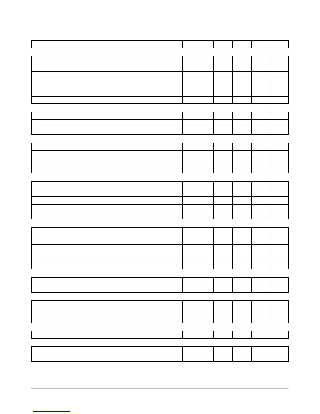
MAXIMUM RATINGS (T
J
= 25°C unless otherwise noted)
Rating
Symbol
Value
Unit
Power Supply Voltage, Pin 6 V
CC
−0.3, 16 V
Input/Output Pins
Pins 1, 2, 3, 5
V
IO
−0.3, 6.5 V
Maximum Voltage on Pin 8 (HV) V
HV
500 V
Thermal Resistance, Junction−to−Air, PDIP−8 Version
Thermal Resistance, Junction−to−Air, SOIC Version
R
q
JA
R
q
JA
100
178
°C/W
°C/W
Operating Junction Temperature Range T
J
−40 to +150 °C
Operating Ambient Temperature Range T
A
−25 to +125 °C
Storage Temperature Range T
stg
−55 to +150 °C
ESD Capability, HBM (All pins except VCC and HV pins) (Note 1) − 2.0 kV
ESD Capability, Machine Model (All pins except VCC and HV pins) (Note 1) − 200 V
Maximum ratings are those values beyond which device damage can occur. Maximum ratings applied to the device are individual stress limit
values (not normal operating conditions) and are not valid simultaneously . If these limits are exceeded, device functional operation is not implied,
damage may occur and reliability may be affected.
1. This device series contains ESD protection and exceeds the following tests:
Human Body Model (HBM) > 2.0 kV per JEDEC standard: JESD22−A114.
Machine Model (MM) > 200 V per JEDEC standard: JESD22−A115.
2. Latchup Current Maximum Rating: ±150 mA per JEDEC standard: JESD78.
Page 5
NCP1201
http://onsemi.com
5
ELECTRICAL CHARACTERISTICS (For typical values T
J
= 25°C, for min/max values TJ = −25°C to +125°C,
V
CC
= 11 V unless otherwise noted)
Characteristic
Symbol Min Typ Max Unit
DYNAMIC SELF−SUPPLY
V
CC
Increasing Level at which the Current Source Turns−Off VCC
OFF
11.5 12.5 13.5 V
VCC Decreasing Level at which the Current Source Turns−On VCC
ON
9.6 10.5 11.3 V
Internal IC Current Consumption, No Output Load on Pin 5 I
CC1
440 905 1300
mA
Internal IC Current Consumption, 1.0 nF Output Load on Pin 5
NCP1201P60, NCP1201D60
NCP1201P100, NCP1201D100
I
CC2
0.75
1.6
1.6
2.1
2.2
2.8
mA
Internal IC Current Consumption, Latchoff Phase I
CC3
405 575 772
mA
INTERNAL STARTUP CURRENT SOURCE
High−Voltage Current Source at V
CCON
– 0.2 V I
C1
3.6 5.3 7.1 mA
High−Voltage Current Source at VCC = 0 V I
C2
7.5 11.1 15 mA
HV Pin Leakage Current @ 450 V, VCC Pin Connected to Ground I
LEAK
− 30 70
mA
OUTPUT SECTION
Output Voltage Rise−Time (CL = 1.0 nF, 10 V Output)
Tr − 116 − ns
Output Voltage Fall−Time (CL = 1.0 nF, 10 V Output) Tf − 41 − ns
Source Resistance (V
DRV
= ) R
OH
26 38 60
W
Sink Resistance (V
DRV
= ) R
OL
4.0 10 22
W
CURRENT SENSE SECTION (Pin 5 Unloaded)
Input Bias Current @ 1.0 V Input Level on Pin 3
I
IB−CS
− 10 100 nA
Maximum Current Sense Input Threshold V
ILIMIT
0.8 0.9 1.0 V
Default Current Sense Threshold for Skip Cycle Operation V
ILSKIP
250 325 390 mV
Propagation Delay from Current Detection to Gate OFF State T
DEL
35 65 160 ns
Leading Edge Blanking Duration T
LEB
150 260 400 ns
OSCILLATOR SECTION (VCC = 11 V, Pin 5 Loaded by 1.0 KW)
Oscillation Frequency
NCP1201P60, NCP1201D60
NCP1201P100, NCP1201D100
F
OSC
52
92
60
100
72
117
kHz
Built−in Frequency Jittering (as a function of Vcc voltage)
NCP1201P60, NCP1201D60
NCP1201P100, NCP1201D100
F
jitter
−
−
493
822
−
−
Hz/V
Maximum Duty Cycle D
max
74 83 87 %
FEEDBACK SECTION (VCC = 11 V, Pin 5 Unloaded)
Internal Pullup Resistor
R
UP
10 17 24
kW
Feedback Pin to Pin 3 Current Setpoint Division Ratio I
ratio
2.9 3.3 4.0 −
BROWNOUT DETECT SECTION
BOK Input Threshold Voltage
V
th
1.75 1.92 2.05 V
BOK Input Bias Current (V
BOK
< Vth) I
IB−BOK
− 11 100 nA
Source Bias Current (Turn on After V
BOK
> Vth) I
SC
40 50 58
mA
FREQUENCY SKIP CYCLE SECTION
Built−in Frequency Skip Cycle Comparator Voltage Threshold
V
SKIP
0.96 1.07 1.18 V
THERMAL SHUTDOWN
Thermal Shutdown Trip Point, Temperature Rising (Note 3)
T
SD
− 145 − °C
Thermal Shutdown Hysteresis T
HYST
− 25 − °C
3. Verified by design.
Page 6
NCP1201
http://onsemi.com
6
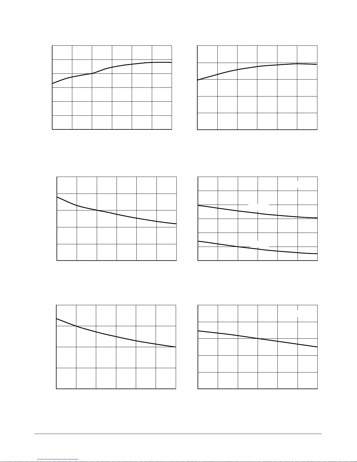
TYPICAL CHARACTERISTICS
TJ, JUNCTION TEMPERATURE (°C)
1251007550250−25
12.9
VCC
OFF
, V
CC
OFF THRESHOLD VOLTAGE (V)
12.5
12.3
11.9
11.7
12.1
12.7
TJ, JUNCTION TEMPERATURE (°C)
1251007550250−25
1100
I
CC1
, CURRENT CONSUMPTION
WITH NO LOAD (mA)
1000
800
700
600
T
J
, JUNCTION TEMPERATURE (°C)
12
5
1007550250−25
2.6
I
CC2
, CURRENT CONSUMPTION (mA)
2.2
2.0
1.6
1.4
1.8
2.4
900
TJ, JUNCTION TEMPERATURE (°C)
12
5
1007550250−25
8.0
I
C1
, HV PIN STARTUP CURRENT
SOURCE (mA)
5.0
3.5
2.0
0.5
6.5
VCC = 11 V
1 nF Load
Figure 3. VCC OFF Threshold Voltage
vs. Junction Temperature
TJ, JUNCTION TEMPERATURE (°C)
12
5
1007550250−25
10.8
VCC
ON
, V
CC
ON THRESHOLD VOLTAGE (V)
10.2
10
9.8
10.4
10.6
Figure 4. VCC ON Threshold Voltage
vs. Junction Temperature
Figure 5. IC Current Consumption, I
CC1
vs. Junction Temperature
Figure 6. IC Current Consumption, I
CC2
vs. Junction Temperature
Figure 7. IC Current Consumption at Latchoff Phase
vs. Junction Temperature
Figure 8. HV Pin Startup Current Source
vs. Junction Temperature
100 KHz
60 KHz
TJ, JUNCTION TEMPERATURE (°C)
1251007550250−25
700
I
CC3
, IC CURRENT CONSUMPTION
AT LATCHOFF PHASE (mA)
600
500
400
300
Page 7

NCP1201
http://onsemi.com
7
TYPICAL CHARACTERISTICS
Figure 9. HV Pin Startup Current Source
vs. Junction Temperature
Figure 10. Leakage Current vs.
Junction Temperature
Figure 11. Output Source Resistance
vs. Junction Temperature
Figure 12. Output Sink Resistance
vs. Junction Temperature
Figure 13. CS Pin Input Bias Current @ 1.0 V
vs. Junction Temperature
Figure 14. Maximum Current Sense Threshold
vs. Junction Temperature
TJ, JUNCTION TEMPERATURE (°C)
1251007550250−25
12
I
IB−CS
, CS PIN INPUT BIAS CURRENT (nA)
10
9
7
6
8
11
TJ, JUNCTION TEMPERATURE (°C)
1251007550250−25
70
R
OH
, SOURCE RESISTANCE (W)
60
40
30
0
T
J
, JUNCTION TEMPERATURE (°C)
12
5
1007550250−25
20
R
OL
, SINK RESISTANCE (W)
16
12
4
0
8
50
T
J
, JUNCTION TEMPERATURE (°C)
12
5
1007550250−25
1.00
V
ILIMIT
, MAXIMUM CURRENT SENSE THRESHOLD (V)
0.96
0.88
0.84
0.80
0.92
20
10
TJ, JUNCTION TEMPERATURE (°C)
1251007550250−25
14
I
C2
, HV PIN STARTUP CURRENT
SOURCE (mA)
12
8
6
4
10
VCC = 0 V
TJ, JUNCTION TEMPERATURE (°C)
12
5
1007550250−25
80
I
LEAK
, LEAKAGE CURRENT (mA)
60
40
20
0
Page 8

NCP1201
http://onsemi.com
8
TYPICAL CHARACTERISTICS
Figure 15. Default Current Setpoint for Skip Cycle
vs. Junction Temperature
Figure 16. Propagation Delay from Current Detection to
Gate Driver vs. Junction Temperature
Figure 17. Leading Edge Blanking Duration
vs. Junction Temperature
Figure 18. Oscillator Frequency
vs. Junction Temperature
Figure 19. Frequency Jittering
vs. Junction Temperature
TJ, JUNCTION TEMPERATURE (°C)
12
5
1007550250−25
100
T
DEL
, PROPAGATION DELAY (nS)
85
55
40
10
T
J
, JUNCTION TEMPERATURE (°C)
1251007550250−25
400
T
LEB
, LEADING EDGE BLANKING
DURATION (nS)
250
100
0
50
300
T
J
, JUNCTION TEMPERATURE (°C)
12
5
1007550250−25
120
F
OSC
, OSCILLATOR FREQUENCY (kHz)
100
40
0
T
J
, JUNCTION TEMPERATURE (°C)
1251007550250−25
1400
F
jitter
, FREQUENCY JITTER (Hz/V)
800
600
200
0
400
60
T
J
, JUNCTION TEMPERATURE (°C)
12
5
1007550250−25
85
D
max
, MAXIMUM DUTY CYCLE (%)
84
82
80
79
83
20
81
70
25
150
200
350
Figure 20. Maximum Duty Cycle
vs. Junction Temperature
80
100 KHz
60 KHz
1200
1000
100 KHz
60 KHz
TJ, JUNCTION TEMPERATURE (°C)
1251007550250−25
340
V
ILSKIP
, DEFAULT CURRENT SENSE
THRESHOLD FOR SKIP CYCLE (mV)
320
310
290
300
330
Page 9

NCP1201
http://onsemi.com
9
TYPICAL CHARACTERISTICS
Figure 21. FB Pin Pullup Resistor
vs. Junction Temperature
Figure 22. Feedback Pin to Pin 3 Current Setpoint Rati
o
vs. Junction Temperature
Figure 23. BOK Threshold Voltage
vs. Junction Temperature
Figure 24. BOK Input Bias Current
vs. Junction Temperature
Figure 25. BOK Source Bias Current
vs. Junction Temperature
Figure 26. Skip Mode Threshold Voltage
vs. Junction Temperature
TJ, JUNCTION TEMPERATURE (°C)
12
5
1007550250−25
1.15
V
SKIP
, SKIP CYCLE COMPARATOR
THRESHOLD VOLTAGE (V)
1.10
1.05
1.00
0.95
T
J
, JUNCTION TEMPERATURE (°C)
1251007550250−25
19
R
UP
, INTERNAL PULLUP RESISTOR (kW)
18
16
13
T
J
, JUNCTION TEMPERATURE (°C)
1251007550250−25
51
I
SC
, BOK BIAS CURRENT (mA)
50
49
46
45
47
17
T
J
, JUNCTION TEMPERATURE (°C)
1251007550250−25
2.00
V
th
, BOK INPUT THRESHOLD VOLTAGE (V)
1.95
1.85
1.75
1.70
T
J
, JUNCTION TEMPERATURE (°C)
12
5
1007550250−25
12
I
IB−BOK
, BOK INPUT BIAS CURRENT (nA)
9
8
7
6
101.90
15
14
11
48
V
BOK
< V
th
1.80
V
BOK
< V
th
TJ, JUNCTION TEMPERATURE (°C)
12
5
1007550250−25
3.40
I
ratio
, FEEDBACK PIN TO PIN 3
CURRENT RATIO
3.20
3.10
3.05
3.00
3.30
3.15
3.25
3.35
Page 10

NCP1201
http://onsemi.com
10
DETAILED OPERATING DESCRIPTION
Introduction
The NCP1201 implements a standard current mode
architecture where the s witch− of f time i s d ictated by the p eak
current setpoint. This component represents the ideal
candidate where low part−count is the key criteria,
particularly in low− cost A C−DC adapters, auxiliary supplies
etc. Due to its high−performance High−Voltage technology,
the NCP1201 incorporates all the necessary components
normally needed in UC384X based supplies: timing
components, feedback devices, low−pass filter and
self−supply. This later point emphasizes the fact that
ON Semiconductor’s NCP1201 does NOT need a n a uxiliary
winding to operate: the device is self supplied from the
high−voltage rail and delivers a V
CC
to the IC. This system
is named the Dynamic Self−Supply (DSS).
Dynamic Self−Supply
The DSS principle is based on the charge/discharge of t h e
V
CC
bulk capacitor from a low level up to a higher level. W e
can easily describe the current source operation following
simple logic equations:
POWER−ON: IF V
CC
< V
CCOFF
THEN
Current Source is ON, no output pulses
IF VCC decreasing > V
CCON
THEN
Current Source is OFF, output is pulsing
IF VCC increasing < V
CCOFF
THEN
Current Source is ON, output is pulsing
Typical values are: V
CCOFF
= 12.5 V, V
CCON
= 10.5 V
To better understand the operation principle, Figure 27
sketch offers the necessary explanation,
Figure 27. The Charge/Discharge Cycle Over a 10 mF VCC Capacitor
10 mS 30 mS 50 mS 70 mS 90 mS
Current
Source
OFF
V
CC
Output Pulses
Vripple = 2 V
VCC
OFF
= 12.5 V
VCCON = 10.5 V
ON
The DSS behavior actually depends on the internal IC
consumption and the MOSFET’s gate charge Qg. If we
select a MOSFET like the MTP2N60E, Qg max equals
22 nC. With a maximum switching frequency of 70 kHz for
the oscillator 60 kHz, the average power necessary to drive
the MOSFET (excluding the driver efficiency and
neglecting various voltage drops) is:
P
driver
+ F
sw(max)
Qg V
CC
(eq. 1)
Where,
P
driver
= Average Power to drive the MOSFET
F
sw(max)
= Maximum switching frequency
Qg = MOSFET’s gate charge
V
CC
= VGS level applied to the gate of the MOSFET
To obtain an estimation of the driving current, simply
divide Pdriver by V
CC
,
I
driver
+ F
sw(max)
Qg+ 1.54 mA
(eq. 2)
The total standby power consumption at no−load will
therefore heavily rely on the internal IC current
consumption plus the driving current (altered by the driver’s
efficiency). Suppose that the IC is supplied from a 350 VDC
line. The current flowing through pin 8 is a direct image of
the NCP1201 current consumption (neglecting the
switching losses of the HV current source). If I
CC2
equals
2.1 mA @ T
A
= 25°C, then the power dissipated (lost) by the
IC is simply: 350 V x 2.1 mA = 735 mW. For design and
reliability reasons, it would be interesting to reduce this
source of wasted power. In order to achieve that, different
methods can be used.
1. Use a MOSFET with lower gate charge Qg;
2. Connect pin through a diode (1N4007 typically) to
one of the mains input. The average value on pin 8
becomes:
V
mainsPEAK
2
p
(eq. 3)
Page 11
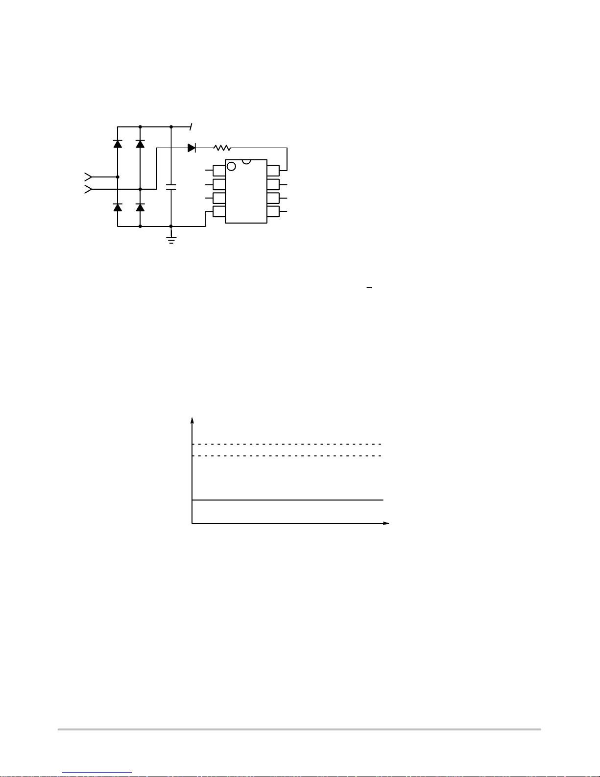
NCP1201
http://onsemi.com
11
Our power contribution example drops to 223 V x 2.1 m
= 468.3 mW. If a resistor is installed between the mains and
the diode, you further force the dissipation to migrate from
the package to the resistor. The resistor value should be
carefully selected to account for low−line startup.
1
2
3
4
8
7
6
5
Figure 28. A Simple Diode Naturally Reduces the
Average Voltage on Pin 8
Mains
HV
Cbulk
3. Permanently force the VCC level above VCC
OFF
with an auxiliary winding. It will automatically
disconnect the internal startup source and the IC
will be fully self−supplied from this winding.
Again, the total power drawn from the mains will
significantly decrease. By using this approach,
user need to make sure the auxiliary voltage never
exceeds the 16 V limit for all line conditions.
Skipping Cycle Mode
The NCP1201 automatically skips switching cycles when
the output power demand drops below a preset level. This is
accomplished by monitoring the FB pin. In normal
operation, FB pin imposes a peak current according to the
load value. If the load demand decreases, the internal loop
asks for less peak current. When this set−point reaches the
skip mode threshold level, 1.07 V, the IC prevents the
current from decreasing further down and starts to blank the
output pulses, i.e. the controller enters the so−called Skip
Cycle Mode, also named Controlled Burst Operation. The
power transfer now depends upon the width of the pulse
bunches, Figure 29.
Suppose we have the following component values:
Lp, primary inductance = 1.0 mH
F
sw
, switching frequency = 60 kHz
Ip (skip) = 200 mA (or 333 mV/R
sense
)
The theoretical power transfer is therefore:
1
2
Lp I
p
2
Fsw+ 1.2 W
(eq. 4)
If the c ontroller e nters Skip C ycle M ode with a p ulse packet
length of 20 ms over a recurrent period of 100 ms, then the
total power transfer reduced to 1.2 W x 0.2 = 240 mW.
To better understand how this Skip Cycle Mode takes
place, a look at the operation mode versus the FB pin voltage
level shown below, immediately gives the necessary insight.
1.07 V
4.2 V, FB Pin Open
FB
Normal Current Mode Operation
Skip Cycle Operation
I
p(min)
= 333 mV / R
sense
Figure 29. Feedback Pin Voltage and Modes of Operation
2.97 V, Upper Dynamic Range
When FB p in v oltage l evel i s a bove t he s kip c ycle t hreshold
(1.07 V by default), the peak current cannot exceed
0.9 V/R
sense
. When the IC enters the skip cycle mode, the
peak current cannot go below V
SKIP
/3.3. By using the peak
current limit reduction scheme, the skip cycle takes place at
a lower peak current, which guarantees noise free operation.
Page 12

NCP1201
http://onsemi.com
12
Figure 30. MOSFET VDS at Various Power Levels, P1<P2<P3
P1 = 0.4 W
P2 = 1.8 W
P
3
= 3.6 W
315.4uS
882uS 1.450mS 2.017mS
2.585mS
300.0M
200.0M
100.0M
0
Skip Cycle
current limit
Max peak
current
Figure 31. The Skip Cycle Takes Place at Low Peak Current
Page 13

NCP1201
http://onsemi.com
13
Brownout Detect Protection
In order to avoid output voltage bouncing during
electricity brownout, a Bulk Capacitor Voltage Comparator
with programmable hysteresis is included in this device. The
non−inverting input, pin 1, is connected to the voltage
divider comprised of R
Upper
and R
Lower
as shown in
Figure 32, monitoring the bulk capacitor voltage level. The
inverting input is connected to a threshold voltage of 1.92 V
internally. As bulk capacitor voltage drops below the
pre−programmed level, i.e. Pin 1 voltage drops below
1.92 V, a reset signal will be generated via internal
protection logic to the PWM Latch to turn off the Power
Switch immediately. At the same time, an internal current
source controlled by the state of the comparator provides a
mean to setup the voltage hysteresis through injecting
current into R
Lower
. The equations below (Equations 5 and
6) show the relationship between V
BULK
levels and the
voltage divider network resistors.
Equations for resistors selection are:
R
Upper
) R
Lower
+
(V
BULK_H
* V
BULK_L
)
50 mA
(eq. 5)
R
Lower
+
[1.92 V(V
BULK_H
* V
BULK_L
)]
(50 mA V
BULK_H
)
(eq. 6)
Assume V
BULK_H
= 90 Vdc and V
BULK_L
= 80 Vdc, by
using 4.3 kW for R
Lower
then R
Upper
is about 195.7 kW.
Figure 32. Brown−Out Protection Operation
R
Upper
V
BULK
R
Lower
BOK
V
REF
50 mA
+
1.92 V
UVLO
−
Page 14
NCP1201
http://onsemi.com
14
APPLICATION INFORMATION
Power Dissipation
The NCP1201 can be directly supplied from the DC rail
through the internal DSS circuitry. The average current
flowing through the DSS is therefore the direct image of the
NCP1201 current consumption. The total power dissipation
can be evaluated using:
(V
HVDC
* 11 V) I
CC2
. If the
device operates on a 250 VAC rail, the maximum rectified
voltage can go up to 350 VDC. At T
A
= 25°C, I
CC2
= 2.1 mA
for the 60 kHz version over a 1.0 nF capacitive load. As a
result, the NCP1201 will dissipate 350 V x 2.1 mA =
735 mW (TA = 25_C). The SOIC−8 package offers a
junction−to−ambient thermal resistance R
q
J−A
of 178°C/W.
Adding some copper area around the device pins will help
to improve this number, 12mm x 12mm copper can drop
R
q
J−A
down to 100°C/W with 35 m copper thickness (1 oz.)
or 6.5mm x 6.5mm with 70 m copper thickness (2 oz.). With
this later number, we can compute the maximum power
dissipation the package accepts at an ambient of 50°C:
P
max
+
T
jmax−TAmax
R
qJ−A
+ 750 mW (T
Jmax
= 125_C),
which is acceptable with our previous thermal budget. For
the DIP8 package, adding a min−pad area of 80mm
2
of 35 m
copper (1 oz.), R
q
J−A
drops from 100°C/W to about 75°C/W.
In the above calculations, I
CC2
is based on a 1.0 nF output
capacitor. As seen before, I
CC2
will depend on your
MOSFET’s Q
g
which I
CC2
≈ I
CC1
+ Fsw x Qg. Final
calculation should thus account for the total gate−charge Q
g
your MOSFET will exhibit.
If the power estimation is beyond the limit, supply to the
V
CC
with a series diode as suggested in Figure 28 can be
used. As a result, it will drop the average input voltage and
lower the dissipation to
350 V 2
p
1.6 mA + 356.5 mW.
Alternatively, an auxiliary winding can be used to disable
the DSS and hence reduce the power consumption down to
VCC x I
CC2
. By using the auxiliary winding supply method,
the rectified auxiliary voltage should permanently stays
above the V
CCOFF
threshold voltage, keeping DSS off and
is safely kept well below the 16 V maximum rating for
whole operating conditions.
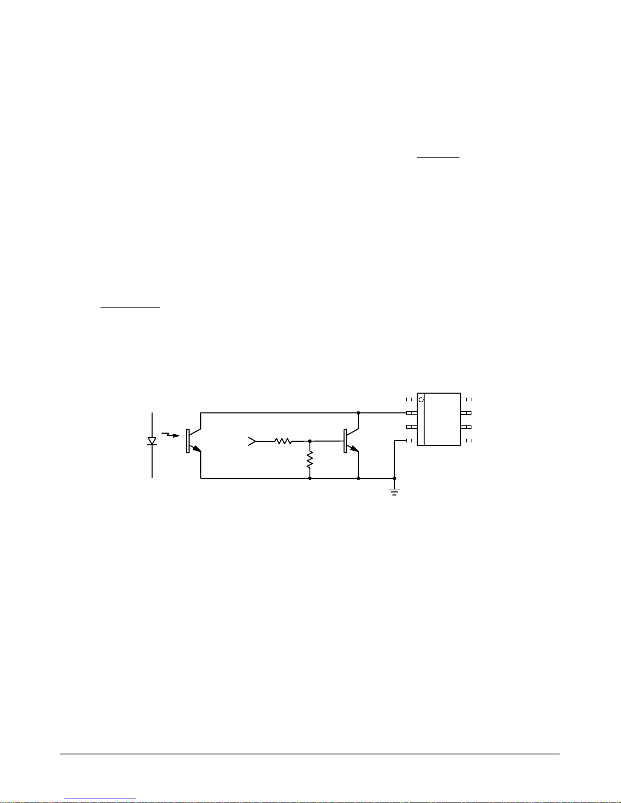
Non−Latching Shutdown
In some cases, it might be desirable to shut off the device
temporarily and authorize its restart once the control signal
has disappeared. This option can easily be accomplished
through a single NPN bipolar transistor wired between FB
and ground. By pulling FB pin voltage below the V
SKIP
level, the output pulses are disabled as long as FB pin
voltage is pulled below the skip mode threshold voltage. As
soon as FB pin is released, the the device resumes its normal
operation again. Figure 33 depicts an application example.
Figure 33. A Method to Shut Down the Device Without a Definitive Latchoff State
ON/OFF
Q1
8
7
6
5
1
2
3
4
Fault Protection
In applications where the output current is purposely not
controlled (e.g. wall adapters delivering raw DC level), it is
often required to permanently latchoff the power supply in
presence of a fault. This fault can be either a short−circuit on
the output or a broken optocoupler. In this later case, it is
important to quickly react in order to avoid a lethal output
voltage runaway. The NCP1201 includes a circuitry tailored
to tackle both events. A short−circuit forces the output
voltage to be at a low level, preventing a bias current to
circulate in the optocoupler LED. As a result, the FB pin
level is pulled up to 4.2 V, as internally imposed by the IC.
The peak current set−point goes to the maximum and the
supply delivers a rather high power with all the associated
effects. However, this can also happen in case of feedback
loss, e.g. a broken optocoupler. To account for those
situations, NCP1201 included a dedicated overload
protection circuitry. Once the protection activated, the
circuitry permanently stops the pulses while the V
CC
moves
between 10−12 V to maintain this latchoff state. The system
resets when the user purposely cycles the V
CC
down below
3.0 V, e.g. when the power plug is removed from the mains.
In NCP1201, the controller stops all output pulses as soon
as the error flag is asserted, irrespective to the V
CC
level.
However, t o avoid false triggers during the startup sequence,
NCP1201 purposely omits the very first V
CC
descent from
12 to 10 V. The error circuitry is actually armed just after this
sequence, e.g. V
CC
crossing 10 V. Figure 34 details the
timing sequence. The V
CC
capacitor should be calculated
carefully to o f fer a su fficient time out during the first startup
V
CC
descent.
Page 15

NCP1201
http://onsemi.com
15
As shown below, the fault logic is armed once VCC crosses
10 V after startup phase. When powering the device from an
auxiliary winding, meeting this condition can sometimes be
problematic since upon startup, V
CC
naturally goes up and
not down as with a DSS. As a result, V
CC
never crosses 10 V
and the fault logic is not activated. If a short−circuit takes
place, the fault circuitry activates as soon as V
CC
collapses
below 10 V (because of the coupling between V
aux
and
V
out
), but in presence of a broken optocoupler, i.e. feedback
is open, V
CC
increases and the fault will never triggered! T o
avoid this problem, the application note “Tips and Tricks
with NCP1200, AN8069/D” offers some possible solutions
where the DSS is kept for protection logic operation only but
all the driving power is derived from the auxiliary winding.
Some solutions even offer the ability to disable the DSS in
standby and benefit to low standby power.
Figure 34. Fault Protection Timing Diagram
Regulation
occurs here
Overload is
not activated
Overload is
activated
Driver
Pulses
Latched−off
Fault occurs here
Regulation
Open−loop
FB level
V
CC
12 V
10 V
No synchronization
between DSS and
fault event
Time
Time
Time
Drv
FB
Calculating the VCC Capacitor
As the above section describes, the fall down sequence
depends upon the V
CC
level, i.e. how long does it take for the
V
CC
line to decrease from 12.5 V to 10.5 V. The required
time depends on the powerup sequence of your system, i.e.
when you first apply the power to the device. The
corresponding transient fault duration due to the output
capacitor charging must be less than the time needed to
discharge from 12.5 V to 10.5 V, otherwise the supply will
not properly startup. The test consists in either simulating or
measuring in the laboratory to determine time required for
the system to reach the regulation at full load. Let’s assume
that this time corresponds to 6.0 ms. Therefore a V
CC
fall
time of 10 ms could be well appropriated in order to not
trigger the overload detection circuitry. If the corresponding
IC consumption, including the MOSFET drive, establishes
at 1.8 mA for instance, we can calculate the required
capacitor using the following formula:
Dt +
DV C
i
, with
DV = 2.0 V. Then for a wanted Dt of 10 ms, C equals 9.0 mF
or 10 mF for a standard value. When an overload condition
occurs, the IC blocks its internal circuitry and its
consumption drops to 575 mA typical. This explains the V
CC
falling slope changes after latchoff in Figure 34.
Page 16

NCP1201
http://onsemi.com
16
Protecting the Controller Against Negative
Spikes
As with any controller built upon a CMOS technology, it
is the designer’s duty to avoid the presence of negative
spikes on sensitive pins. Negative signals have the bad habit
to forward bias the controller substrate and induce erratic
behaviors. Sometimes, the injection can be so strong that
internal parasitic SCRs are triggered, engendering
irremediable damages to the IC if they are a low impedance
path is offered between V
CC
and GND. If the current sense
pin is often the seat of such spurious signals, the
high−voltage pin can also be the source of problems in
certain circumstances. During the turn−off sequence, e.g.
when the user unplugs the power supply, the controller is still
fed by its V
CC
capacitor and keeps activating the MOSFET
ON and OFF with a peak current limited by Rsense.
Unfortunately , if the quality coefficient Q of the resonating
network formed by Lp and Cbulk is low (e.g. the MOSFET
Rdson + Rsense are small), conditions are met to make the
circuit resonate and thus negatively bias the controller . Since
we are talking about ms pulses, the amount of injected
charge (Q = I x t) immediately latches the controller which
brutally discharges its V
CC
capacitor. If this VCC capacitor
is of sufficient value, its stored energy damages the
controller. Figure 35 depicts a typical negative shot
occurring on the HV pin where the brutal V
CC
discharge
testifies for latchup.
Figure 35. A negative spike takes place on the Bulk capacitor at the switch−off sequence
Simple and inexpensive cures exist to prevent from
internal parasitic SCR activation. One of them consists in
inserting a resistor in series with the high−voltage pin to
keep the negative current to the lowest when the bulk
becomes negative (Figure 36). Please note that the negative
spike is clamped to –2 x Vf due to the diode bridge. Please
refer to AND8069 for power dissipation calculations.
Another option (Figure 37) consists in wiring a diode from
V
CC
to the bulk capacitor to force VCC to reach UVLOlow
sooner and thus stops the switching activity before the bulk
capacitor gets deeply discharged. For security reasons, two
diodes can be connected in series.
Figure 36. A simple resistor in series avoids any
latchup in the controller
CV
CC
D3
1N4007
8
7
6
5
1
2
3
4
+
Cbulk
+
1
3
CV
CC
Rbulk
> 4.7 k
8
7
6
5
1
2
3
4
+
Cbulk
+
1
2
3
Figure 37. or a diode forces VCC to reach
UVLOlow sooner
Page 17

NCP1201
http://onsemi.com
17
ORDERING INFORMATION
Device Package Shipping
†
NCP1201P60 PDIP−8
50 Units / Rail
NCP1201P60G PDIP−8
(Pb−Free)
NCP1201D60R2 SOIC−8
2500 Units / Tape & Reel
NCP1201D60R2G SOIC−8
(Pb−Free)
NCP1201P100 PDIP−8
50 Units / Rail
NCP1201P100G PDIP−8
(Pb−Free)
NCP1201D100R2 SOIC−8
2500 Units / Tape & Reel
NCP1201D100R2G SOIC−8
(Pb−Free)
†For information on tape and reel specifications, including part orientation and tape sizes, please refer to our Tape and Reel Packaging
Specifications Brochure, BRD8011/D.
Page 18

NCP1201
http://onsemi.com
18
PACKAGE DIMENSIONS
SOIC−8 NB
CASE 751−07
ISSUE AG
SEATING
PLANE
1
4
58
N
J
X 45
_
K
NOTES:
1. DIMENSIONING AND TOLERANCING PER
ANSI Y14.5M, 1982.
2. CONTROLLING DIMENSION: MILLIMETER.
3. DIMENSION A AND B DO NOT INCLUDE
MOLD PROTRUSION.
4. MAXIMUM MOLD PROTRUSION 0.15 (0.006)
PER SIDE.
5. DIMENSION D DOES NOT INCLUDE DAMBAR
PROTRUSION. ALLOWABLE DAMBAR
PROTRUSION SHALL BE 0.127 (0.005) TOTAL
IN EXCESS OF THE D DIMENSION AT
MAXIMUM MATERIAL CONDITION.
6. 751−01 THRU 751−06 ARE OBSOLETE. NEW
STANDARD IS 751−07.
A
B
S
D
H
C
0.10 (0.004)
DIMAMIN MAX MIN MAX
INCHES
4.80 5.00 0.189 0.197
MILLIMETERS
B 3.80 4.00 0.150 0.157
C 1.35 1.75 0.053 0.069
D 0.33 0.51 0.013 0.020
G 1.27 BSC 0.050 BSC
H 0.10 0.25 0.004 0.010
J 0.19 0.25 0.007 0.010
K 0.40 1.27 0.016 0.050
M 0 8 0 8
N 0.25 0.50 0.010 0.020
S 5.80 6.20 0.228 0.244
−X−
−Y−
G
M
Y
M
0.25 (0.010)
−Z−
Y
M
0.25 (0.010) Z
SXS
M
____
1.52
0.060
7.0
0.275
0.6
0.024
1.270
0.050
4.0
0.155
ǒ
mm
inches
Ǔ
SCALE 6:1
*For additional information on our Pb−Free strategy and soldering
details, please download the ON Semiconductor Soldering and
Mounting Techniques Reference Manual, SOLDERRM/D.
SOLDERING FOOTPRINT*
Page 19

NCP1201
http://onsemi.com
19
PACKAGE DIMENSIONS
NOTES:
1. DIMENSION L TO CENTER OF LEAD WHEN
FORMED PARALLEL.
2. PACKAGE CONTOUR OPTIONAL (ROUND OR
SQUARE CORNERS).
3. DIMENSIONING AND TOLERANCING PER ANSI
Y14.5M, 1982.
14
58
F
NOTE 2
−A−
−B−
−T−
SEATING
PLANE
H
J
G
D
K
N
C
L
M
M
A
M
0.13 (0.005) B
M
T
DIM MIN MAX MIN MAX
INCHESMILLIMETERS
A 9.40 10.16 0.370 0.400
B 6.10 6.60 0.240 0.260
C 3.94 4.45 0.155 0.175
D 0.38 0.51 0.015 0.020
F 1.02 1.78 0.040 0.070
G 2.54 BSC 0.100 BSC
H 0.76 1.27 0.030 0.050
J 0.20 0.30 0.008 0.012
K 2.92 3.43 0.115 0.135
L 7.62 BSC 0.300 BSC
M −−− 10 −−− 10
N 0.76 1.01 0.030 0.040
__
8 LEAD PDIP
CASE 626−05
ISSUE L
ON Semiconductor and are registered trademarks of Semiconductor Components Industries, LLC (SCILLC). SCILLC reserves the right to make changes without further notice
to any products herein. SCILLC makes no warranty, representation or guarantee regarding the suitability of its products for any particular purpose, nor does SCILLC assume any liability
arising out of the application or use of any product or circuit, and specifically disclaims any and all liability, including without limitation special, consequential or incidental damages.
“Typical” parameters which may be provided in SCILLC data sheets and/or specifications can and do vary in different applications and actual performance may vary over time. All
operating parameters, including “Typicals” must be validated for each customer application by customer’s technical experts. SCILLC does not convey any license under its patent rights
nor the rights of others. SCILLC products are not designed, intended, or authorized for use as components in systems intended for surgical implant into the body, or other applications
intended to support or sustain life, or for any other application in which the failure of the SCILLC product could create a situation where personal injury or death may occur. Should
Buyer purchase or use SCILLC products for any such unintended or unauthorized application, Buyer shall indemnify and hold SCILLC and its officers, employees, subsidiaries, affiliates,
and distributors harmless against all claims, costs, damages, and expenses, and reasonable attorney fees arising out of, directly or indirectly, any claim of personal injury or death
associated with such unintended or unauthorized use, even if such claim alleges that SCILLC was negligent regarding the design or manufacture of the part. SCILLC is an Equal
Opportunity/Affirmative Action Employer. This literature is subject to all applicable copyright laws and is not for resale in any manner.
PUBLICATION ORDERING INFORMATION
N. American Technical Support: 800−282−9855 Toll Free
USA/Canada
Japan: ON Semiconductor, Japan Customer Focus Center
2−9−1 Kamimeguro, Meguro−ku, Tokyo, Japan 153−0051
Phone: 81−3−5773−3850
NCP1201/D
The product described herein (NCP1201), may be covered by the following U.S. patents: 6,271,735, 6,362,067, 6,385,060, 6,429,709, 6,587,357. There may
be other patents pending.
LITERATURE FULFILLMENT:
Literature Distribution Center for ON Semiconductor
P.O. Box 61312, Phoenix, Arizona 85082−1312 USA
Phone: 480−829−7710 or 800−344−3860 Toll Free USA/Canada
Fax: 480−829−7709 or 800−344−3867 Toll Free USA/Canada
Email: orderlit@onsemi.com
ON Semiconductor Website: http://onsemi.com
Order Literature: http://www.onsemi.com/litorder
For additional information, please contact your
local Sales Representative.
 Loading...