

Page 1
High-Voltage Switcher for
Low Power Offline SMPS
NCP1060, NCP1063
The NCP106X products integrate a fixed frequency current mode
controller with a 700 V MOSFET. Available in a PDIP−7, SOIC−10 or
SOIC−16 package, the NCP106X offer a high level of integration,
including soft−start, frequency−jittering, short−circuit protection,
skip−cycle, adjustable peak current set point, ramp compensation, and a
Dynamic Self−Supply (eliminating the need for an auxiliary winding).
Unlike other monolithic solutions, the NCP106X is quiet by nature:
during nominal load operation, the part switches at one of the available
frequencies (60 kHz or 100 kHz). When the output power demand
diminishes, the IC automatically enters frequency foldback mode and
provides excellent efficiency at light loads. When the power demand
reduces further, it enters into a skip mode to reduce the standby
consumption down to a no load condition.
Protection features include: a timer to detect an overload or a
short−circuit event, Overvoltage Protection with auto−recovery and
AC input line voltage detection (A version).
The ON proprietary integrated Over Power Protection (OPP) lets
you harness the maximum delivered power without affecting your
standby performance simply via external resistors.
For improved standby performance, the connection of an auxiliary
winding stops the DSS operation and helps to reduce input power
consumption below 50 mW at high line.
NCP106x can be seamlessly used both in non−isolated and in
isolated topologies.
16
www.onsemi.com
MARKING DIAGRAMS
7
PDIP−7
8
1
1
10
1
CASE 626A
AP SUFFIX
SOIC−16
CASE 751B−05
D SUFFIX
SOIC−10
CASE 751BQ
AD or BD SUFFIX
1
16
NCP1063fyyyG
1
10
1
P106xfyyy
AWL
YYWWG
AWLYWW
1060fyyy
ALYWX
G
Features
• Built−in 700 V MOSFET with R
of 34 W (NCP1060) and
DS(on)
11.4 W (NCP1063)
• Large Creepage Distance Between High−voltage Pins
• Current−Mode Fixed Frequency Operation – 60 kHz or 100 kHz
(130 kHz on demand)
• Adjustable Peak Current: see below table
• Fixed Ramp Compensation
• Direct Feedback Connection for Non−isolated Converter
• Internal and Adjustable Over Power Protection (OPP) Circuit
• Skip−Cycle Operation at Low Peak Currents Only
• Dynamic Self−Supply: No Need for an Auxiliary Winding
• Internal 4 ms Soft−Start
• Auto−Recovery Output Short Circuit Protection with Timer−Based
Detection
• Auto−Recovery Overvoltage Protection with Auxiliary Winding
Operation
• Frequency Jittering for Better EMI Signature
• No Load Input Consumption < 50 mW
• Frequency Foldback to Improve Efficiency at Light Load
• These Devices are Pb−Free and are RoHS Compliant
x = Power Switch Circuit
On−state Resistance
(0 = 34 W, 3 = 11.4 W)
f = Brown In (A = Yes, B = No)
yyy = Oscillator Frequency
(060 = 60 kHz, 100 = 100 kHz)
A = Assembly Location
L, WL = Wafer Lot
Y, YY = Year
W, WW = Work Week
G or G = Pb−Free Package
ORDERING INFORMATION
See detailed ordering and shipping information on page 28 of
this data sheet.
Typical Applications
• Auxiliary / Standby Isolated and
Non−isolated Power Supplies
• Power Meter SMPS
• Wide Vin Low Power Industrial SMPS
© Semiconductor Components Industries, LLC, 2014
March, 2021 − Rev. 10
1 Publication Order Number:
NCP1060/D
Page 2
NCP1060, NCP1063
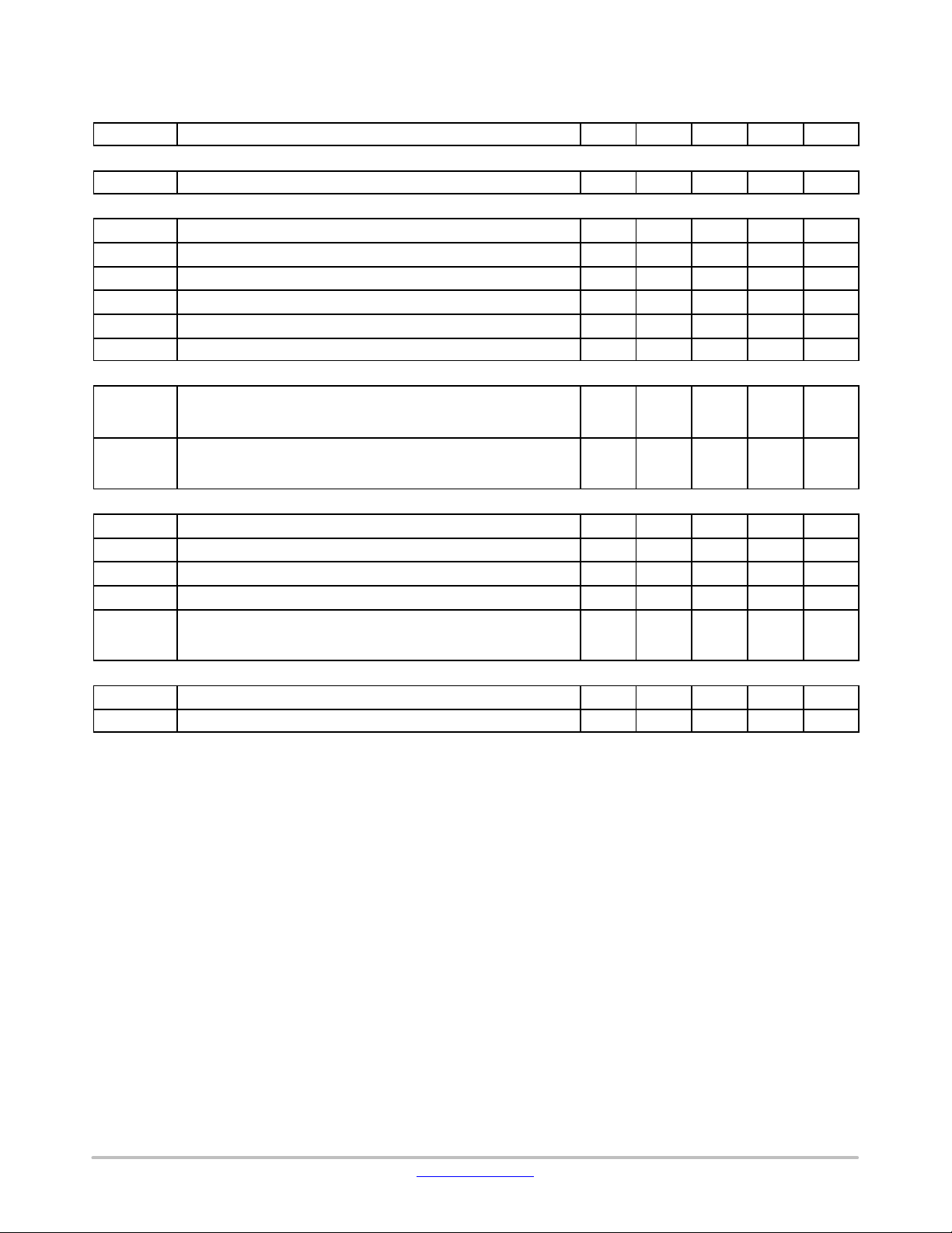
Table 1. PRODUCT INFORMATION & INDICATIVE MAXIMUM OUTPUT POWER
230 Vac + 15% 85 − 265 Vac
Product R
NCP1060 60 kHz
NCP1063 100 kHz
DS(on)
34 W
11.4 W
NOTE: Informative values only, with T
on minimum copper area as recommended.
= 25°C, T
amb
I
IPK(0)
300 mA 3.3 W 8.3 W 1.9 W 4.7 W
780 mA 6.2 W 15.5 W 3.3 W 7.8 W
= 100°C, PDIP−7 package, Self supply via Auxiliary winding and circuit mounted
case
Adapter Open Frame Adapter Open Frame
GND
VCC
LIM/OPP
FB
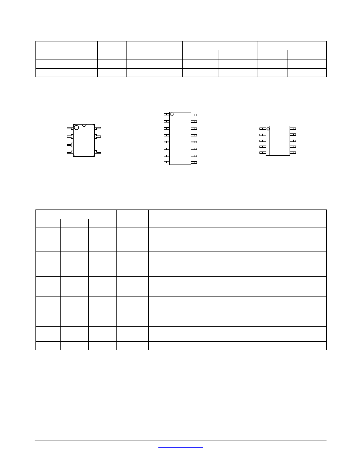
PDIP−7
DRAIN
DRAIN
COMP
GND
GND
GND
GND
VCC
LIM/OPP
FB
COMP
SOIC−16
DRAIN
DRAIN
DRAIN
DRAIN
N.C.
N.C.
N.C.
N.C.
GND
VCC
LIM/OPP
FB
COMP
SOIC−10
Figure 1. Pin Connections
Table 2. PIN FUNCTION DESCRIPTION
Pin No
PDIP 7 SOIC 10 SOIC 16
1 1 1−4 GND The IC Ground
2 2 5 V
3 3 6 LIM/OPP Ipeak set / Over
4 4 7 FB Feedback signal
5 5 8 Comp Compensation The error amplifier output is available on this pin. The
6 9−12 This un−connected pin ensures adequate creepage dis-
7,8 6−10 13−16 Drain Drain connection The internal drain MOSFET connection
Pin Name Function Pin Description
CC
Powers the internal
circuitry
This pin is connected to an external capacitor. The V
includes an auto−recovery over voltage protection.
The current drown from the pin decreases Ipeak of the
power limitation
primary winding. If resistive divider from the auxiliary
winding is connected to this pin it sets the OPP compensation level (it diminishes the peak current.)
This is the inverting input of the trans conductance error
input
amplifier. It is normally connected to the switching power
supply output through a resistor divider.
network connected between this pin and ground adjusts
the regulation loop bandwidth. Also, by connecting an
opto−coupler to this pin, the peak current set point is
adjusted accordingly to the output power demand.
tance
DRAIN
DRAIN
DRAIN
DRAIN
DRAIN
DD
www.onsemi.com
2
Page 3
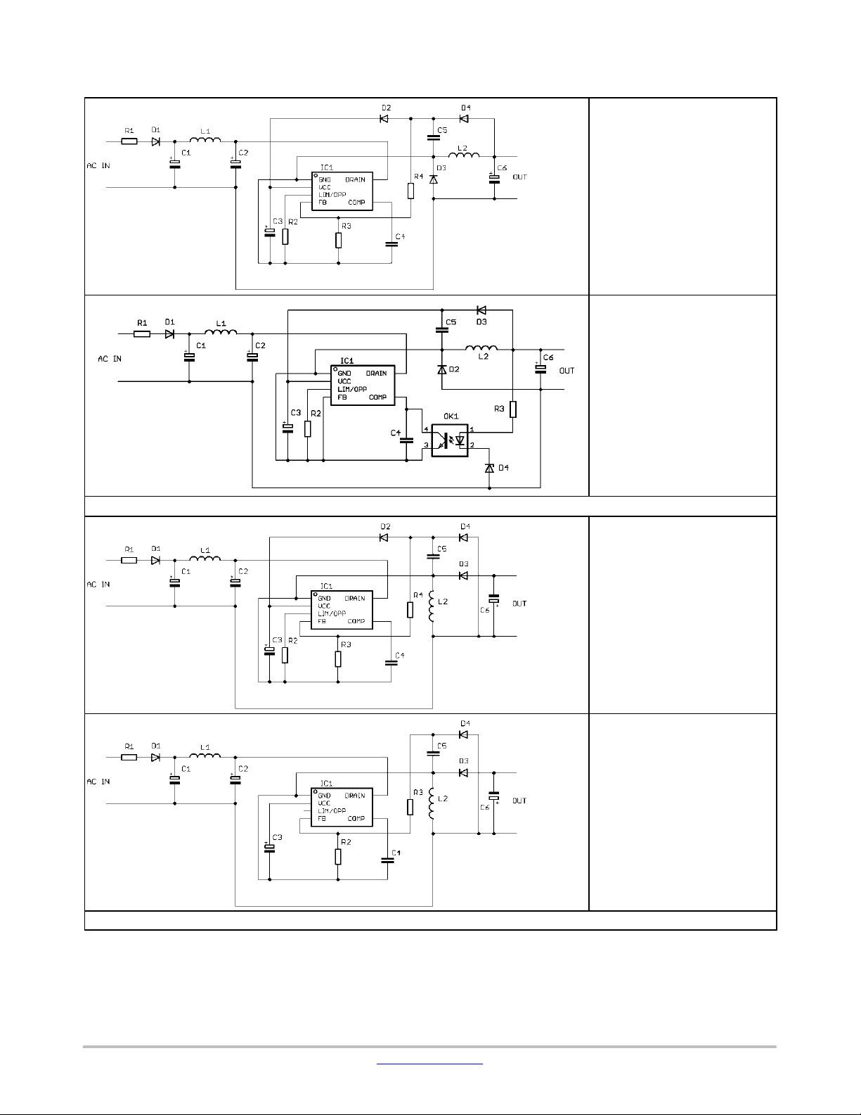
Table 3. TYPICAL APPLICATIONS
NCP1060, NCP1063
• If the output voltage is above
9.0 V typ. (between Vcc(on)
level and Vovp level) Vcc is
supplied from output via D2
• If the output voltage is
below 9.0 V, D2 is redundant,
the IC is supplied from DSS
• R2 limits maximum output
power (can be omitted if not
required)
• Direct feedback, resistive
divider formed by R3, R4 sets
output voltage
• If the output voltage is above
9.0 V typ. (between Vcc(on)
level and Vovp level) Vcc is
supplied from output via D3
• If the output voltage is below
9.0 V, D3 and C5 are
redundant, the IC is supplied
from DSS
• R2 limits maximum output
power (can be omitted if not
required)
• Optocoupler feedback
Typical Non−isolated Application – Buck Converter
• If the output voltage is above
9.0 V typ. between V
level and V
supplied from output via D2
• R2 limits maximal output
power
• Direct feedback, resistive
divider formed by R3, R4 sets
output voltage
• VCC supplied from DSS
• Output voltage is below 9.0 V
typ.
• LIM/OPP pin floating − no limit
output power
• Direct feedback, resistive
divider formed by R2, R3 sets
output voltage
OVP
CC(ON)
level − VCC
Typical Non−isolated Application – Buck−Boost Converter
www.onsemi.com
3
Page 4
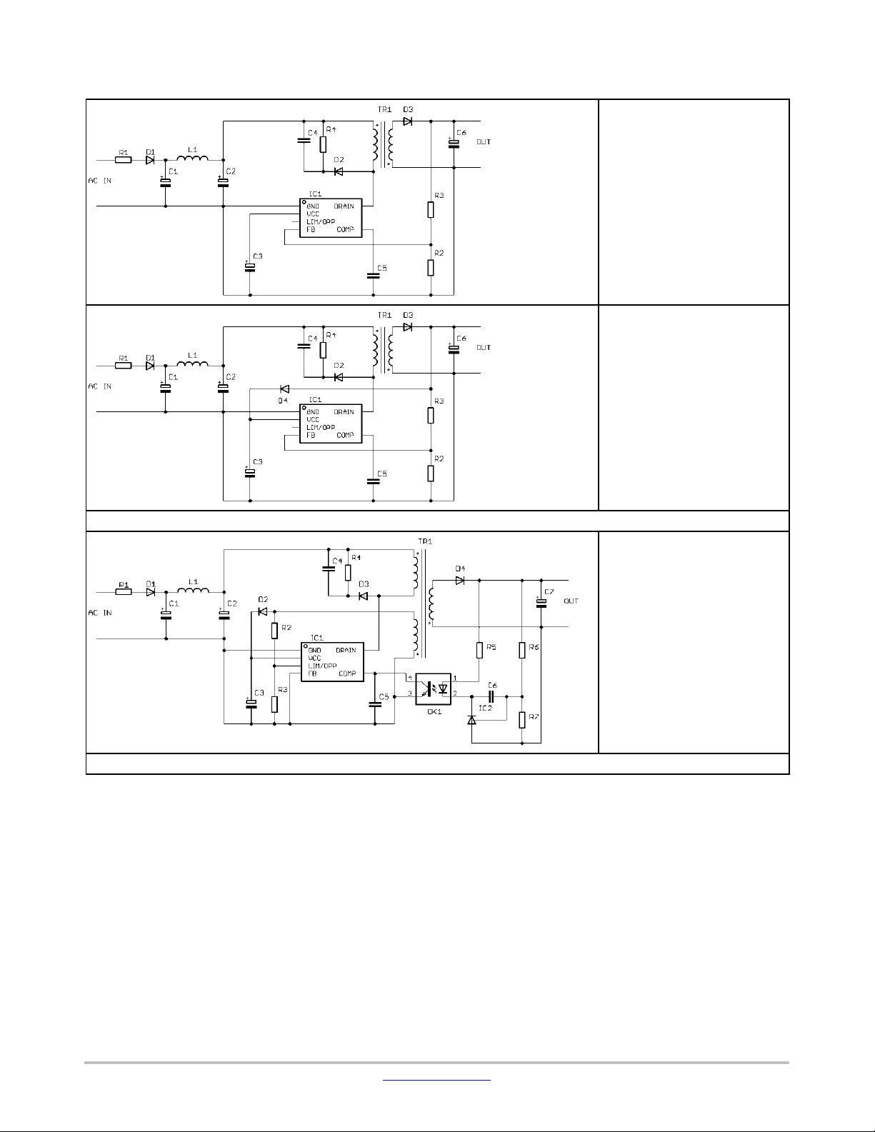
Table 3. TYPICAL APPLICATIONS (continued)
NCP1060, NCP1063
• VCC supplied from DSS
• Output voltage is below 9.0 V
typ.
• LIM/OPP pin floating − no limit
output power
• Resistive divider formed by R2,
R3 sets output voltage
• If the output voltage is above
9.0 V typ. between V
level and V
supplied from output via D4
• LIM/OPP pin floating − no limit
output power
• Resistive divider formed by R2,
R3 sets output voltage
OVP
CC(ON)
level − VCC
Typical Non−isolated Application – Flyback Converter
Typical Isolated Application – Flyback Converter
• VCC supplied from auxiliary
winding
• Resistive divider formed by R2,
R3 sets output power limit and
over power protection
• Optocoupler feedback,
resistive divider formed by R6,
R7 sets output voltage
www.onsemi.com
4
Page 5
NCP1060, NCP1063
VCC
R
COMP(up)
V
COMP(REF )
DRAIN
ms Filter
80−
V
OVP
I
pflag
VCC OVP
SCP
t
SCP
S
Q
R
t
recovery
Jittering
OSC
LineOK
Sawtooth
OFF
TSD
S
Foldback
Q
VCC
Management
LineOK
UVLO
Sawtooth
R
I
COMPskip
SKIP
Ramp
SKIP = ”1”èShut down some
blocks to reduce consumption
compensation
UVLO
Reset
V
dd
OFF UVLO
Line
Detection
V
CC
LEB
GND
COMP
FB
I
FB
FB/COMP
Processing
I
I
COMPfault
I
to CS setpoint
COMP
I
LMOP (min)ILMOP (max )
0
I
LMDEC
I
LMDEC
pflag
I
FreezeIpk(0)
I
LMOP
I
PKL
I
LMOP
V
LMOP
LIM/OPP
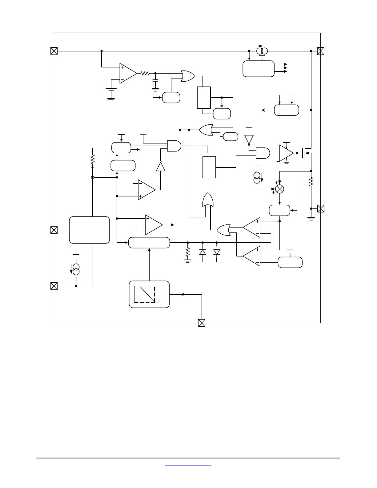
Figure 2. Simplified Internal Circuit Architecture
Reset
Soft−Start
Reset SS as recoving from
SCP, TSD, VCC OVP or UVLO
www.onsemi.com
5
Page 6
NCP1060, NCP1063
Table 4. MAXIMUM RATING TABLE (All voltages related to GND terminal)
Rating
Power supply voltage, V
pin, continuous voltage V
CC
Voltage on all pins, except Drain and VCC pin Vinmax −0.3 to 10 V
Drain voltage BVdss −0.3 to 700 V
Maximum Current into VCC pin I
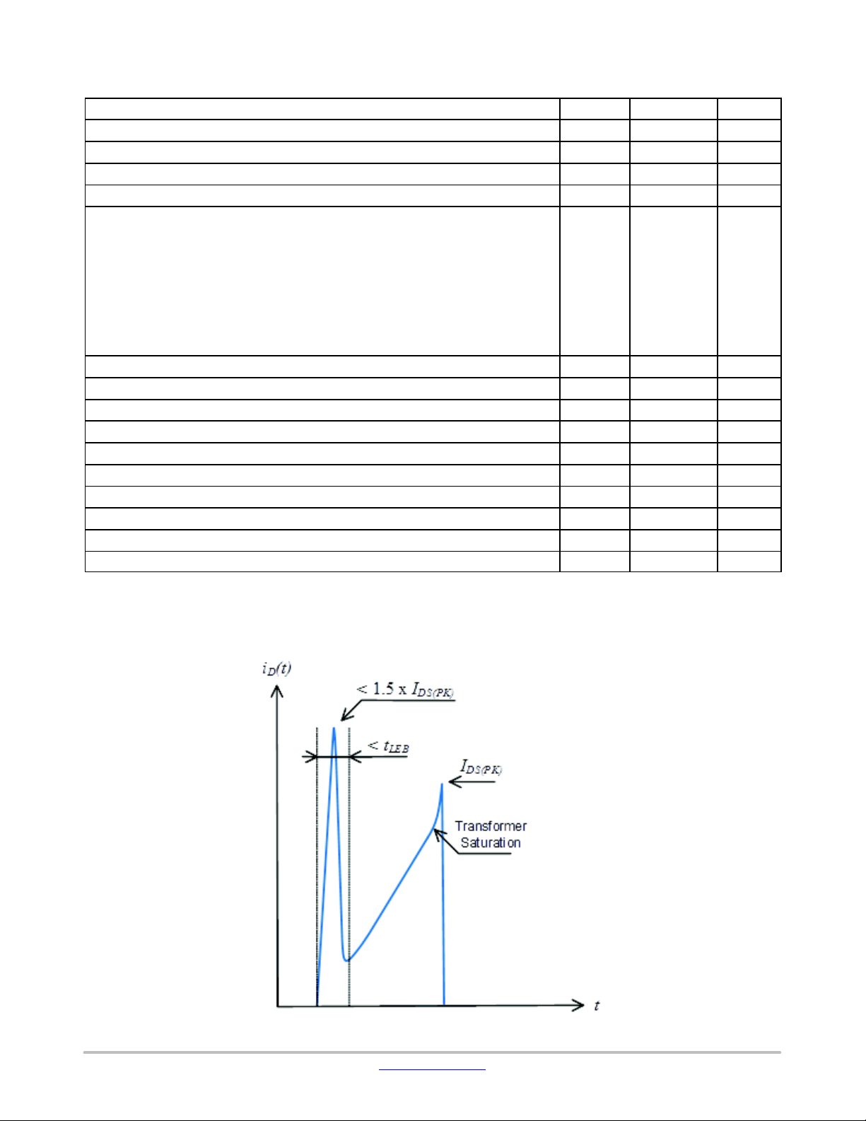
Drain Current Peak during Transformer Saturation (TJ = 150°C, Note 2):
NCP1060
NCP1063
Drain Current Peak during Transformer Saturation (T
= 125°C, Note 2):
J
NCP1060
NCP1063
Drain Current Peak during Transformer Saturation (T
= 25°C, Note 2):
J
NCP1060
NCP1063
Thermal Resistance, Junction−to−Air – PDIP7 with 200 mm@ of 35−m copper area
Thermal Resistance, Junction−to−Air – SOIC10 with 200 mm@ of 35−m copper area
Thermal Resistance, Junction−to−Air – SOIC16 with 200 mm@ of 35−m copper area
Junction−to−Top Thermal Characterization Parameter – PDIP7
Junction−to−Top Thermal Characterization Parameter – SOIC10
Junction−to−Top Thermal Characterization Parameter – SOIC16
Junction Temperature Range T
Storage Temperature Range T
Human Body Model ESD Capability (All pins except HV pin) per JEDEC JESD22−A114F HBM 2 kV
Charged−Device Model ESD Capability per JEDEC JESD22−C101E CDM 1 kV
Stresses exceeding those listed in the Maximum Ratings table may damage the device. If any of these limits are exceeded, device functionality
should not be assumed, damage may occur and reliability may be affected.
1. This device contains latch−up protection and exceeds 100 mA per JEDEC Standard JESD78.
2. Maximum drain current I
on. Figure 3 below provides spike limits the device can tolerate.
is obtained when the transformer saturates. It should not be mixed with short pulses that can be seen at turn
DS(PK)
Symbol Value Unit
CC
CC
I
DS(PK)
−0.3 to 20 V
10 mA
mA
300
850
335
950
520
1500
R
θ
JA
R
θ
JA
R
θ
JA
Y
JT
Y
JT
Y
JT
J
stg
115 °C/W
132 °C/W
104 °C/W
7.3 °C/W
2.3 °C/W
2.5 °C/W
−40 to +150 °C
−60 to +150 °C
Figure 3. Spike Limits
www.onsemi.com
6
Page 7
NCP1060, NCP1063
Table 5. ELECTRICAL CHARACTERISTICS
(For typical values T
Symbol
SUPPLY SECTION AND VCC MANAGEMENT
V
CC(on)
V
CC(min)
V
CC(off)
I
CC1
I
CCskip
POWER SWITCH CIRCUIT
R
DS(on)
BV
DSS
I
DSS(off)
t
r
t
f
t
on(min)
INTERNAL START−UP CURRENT SOURCE
I
start1
I
start2
V
CCTH
V
start(min)
CURRENT COMPARATOR
I
IPK
I
IPK(0)
3. The final switch current is: I
the primary inductor in a flyback, and t
L
P
4. Oscillator frequency is measured with disabled jittering.
= 25°C, for min/max values TJ = −40°C to +125°C, VCC = 14 V unless otherwise noted)
J
Rating Pin Min Typ Max Unit
VCC increasing level at which the switcher starts operation 2 (5) 8.4 9.0 9.5 V
VCC decreasing level at which the HV current source restarts 2 (5) 7.0 7.5 7.8 V
VCC decreasing level at which the switcher stops operation (UVLO) 2 (5) 6.7 7.0 7.2 V
Internal IC consumption, NCP1060 switching at 60 kHz, LIM/OPP = 0 A
Internal IC consumption, NCP1060 switching at 100 kHz, LIM/OPP = 0 A
Internal IC consumption, NCP1063 switching at 60 kHz, LIM/OPP = 0 A
Internal IC consumption, NCP1063 switching at 100 kHz, LIM/OPP = 0 A
Internal IC consumption, COMP is 0 V (No switching on MOSFET) 2 (5) − 340 −
Power Switch Circuit on−state resistance
NCP1060 (Id = 50 mA)
Tj = 25°C
Tj = 125°C
NCP1063 (Id = 50 mA)
Tj = 25°C
Tj = 125°C
Power Switch Circuit & Startup breakdown voltage
= 120 mA, Tj = 25°C)
(ID
(off)
Power Switch & Startup breakdown voltage off−state leakage current
Tj = 125°C (Vds = 700 V)
Switching characteristics (RL = 50 W, VDS set for I
Turn−on time (90% − 10%)
Turn−off time (10% − 90%)
Minimum on time
NCP1060
NCP1063
High−voltage current source, VCC = V
CC(on)
High−voltage current source, VCC = 0 V 7, 8
VCC Transient level for I
start1
to I
toggling point 2 (5) − 1.4 − V
start2
Minimum startup voltage, VCC = 0 V 7, 8
Maximum internal current setpoint at 50% duty cycle
FB = 2 V, LIM/OPP = 0 mA, Tj = 25°C
NCP1060
NCP1063
Maximum internal current setpoint at beginning of switching cycle
FB = 2 V, LIM/OPP pin open Tj = 25°C
NCP1060
NCP1063
/ (Vin/LP + Sa) x Vin/LP + Vin/L
IPK(0)
the propagation delay.
prop
2 (5) −
7, 8
(6−10)
(13−16)
7, 8
(6−10)
(13−16)
7, 8
(6−10)
(13−16)
= 0.7 x Ilim)
drain
7, 8
(6−10)
(13−16)
7, 8
(6−10)
(13−16)
– 200 mV 7, 8
(6−10)
(13−16)
(6−10)
(13−16)
(6−10)
(13−16)
−
−
−
−
x t
, with Sa the built−in slope compensation, Vin the input voltage,
P
prop
0.92
−
−
−
−
−
−
−
0.97
0.99
1.07
34
65
11.4
22
−
−
−
−
41
72
14.0
24
mA
700 − − V
− 84 −
−
−
−
−
20
10
200
230
−
−
−
−
5 8 12 mA
− 0.5 − mA
21 V
mA
−
−
250
650
−
−
mA
268
702
300
780
332
858
mA
W
mA
ns
ns
www.onsemi.com
7
Page 8
NCP1060, NCP1063
Table 5. ELECTRICAL CHARACTERISTICS (continued)
(For typical values T
Symbol UnitMaxTypMinPinRating
CURRENT COMPARATOR
I
IPKSW
I
IPKSW
I
LMDEC
t
SS
t
prop
t
LEB
INTERNAL OSCILLATOR
f
OSC
f
OSC
f
jitter
f
swing
D
max
ERROR AMPLIFIER SECTION
V
REF
I
FB
G
M
I
OTAlim
V
OTAen
COMPENSATION SECTION
I
COMPfault
I
COMP100%
I
COMPfreeze
V
COMP(REF)
R
COMP(up)
V
LMOP
I
LMOP
I
LMOP(min)
I
LMOP(max)
I
LMOP(neg)
3. The final switch current is: I
LP the primary inductor in a flyback, and t
4. Oscillator frequency is measured with disabled jittering.
= 25°C, for min/max values TJ = −40°C to +125°C, VCC = 14 V unless otherwise noted)
J
Final switch current with a primary slope of 200 mA/ms,
F
= 60 kHz (Note 3), LIM/OPP pin open
SW
NCP1060
NCP1063
Final switch current with a primary slope of 200 mA/ms,
F
= 100 kHz (Note 3), LIM/OPP pin open
SW
NCP1060
NCP1063
Maximum internal current setpoint at beginning of switching cycle
FB = 2 V, LIM/OPP = −285 mA, Tj = 25°C
NCP1060
NCP1063
Soft−start duration (guaranteed by design) − − 4 − ms
Propagation delay from current detection to drain OFF state − − 70 − ns
Leading Edge Blanking Duration
NCP1060
NCP1063
Oscillation frequency, 60 kHz version, Tj = 25°C (Note 4) − 54 60 66 kHz
Oscillation frequency, 100 kHz version, Tj = 25°C (Note 4) − 90 100 110 kHz
Frequency jittering in percentage of f
OSC
Jittering swing frequency − − 300 − Hz
Maximum duty−cycle − 62 66 72 %
Voltage Feedback Input (V
= 2.5 V) 4 (7) 3.2 3.3 3.4 V
COMP
Input Bias Current (VFB = 3.3 V) 4 (7) − 1 −
Transconductance 5 (8) 2 mS
OTA maximum current capability (VFB > V
OTAen
FB voltage to disable OTA 4 (7) 0.7 1.3 1.7 V
COMP current for which Fault is detected 5 (8) − −40 −
COMP current for which internal current set−point is 100% (I
COMP current for which internal current setpoint is:
I
Freeze1 or 2
(NCP1060/3)
Equivalent pull−up voltage in linear regulation range
(Guaranteed by design)
Equivalent feedback resistor in linear regulation range
(Guaranteed by design)
Voltage on LIM/OPP pin @ I
Voltage on LIM/OPP pin @ I
= −35 mA
LMOP
= −250 mA, Tj = 25°C
LMOP
Maximum current from LIM/OPP pin 3 (6) −330 −420
Current at which LIM/OPP starts to decrease I
Current at which LIM/OPP stops to decrease I
Negative Active Clamp Voltage (I
/ (Vin/LP + Sa) x Vin/LP + Vin/L
IPK(0)
LMOP
the propagation delay.
prop
PEAK
= −2.5 mA) 3 (6) −0.7 V
−
−
−
−
−
−
−
−
−
−
−
−
−
−
−
−
− − ±6 − %
) 5 (8) ±150
) 5 (8) − −44 −
IPK(0)
5 (8) − −80 −
5 (8) − 2.7 − V
5 (8) − 17.7 −
3 (6) 1.40
1.28
PEAK
3 (6) −20 −26 −32
3 (6) −285
x t
, with Sa the built−in slope compensation, Vin the input voltage,
P
prop
330
740
320
710
128
312
130
160
1.50
1.35
−
−
−
−
−
−
−
−
1.60
1.42
mA
mA
mA
ns
mA
mA
mA
mA
mA
kΩ
V
mA
mA
mA
www.onsemi.com
8
Page 9
NCP1060, NCP1063
Table 5. ELECTRICAL CHARACTERISTICS (continued)
(For typical values T
Symbol UnitMaxTypMinPinRating
COMPENSATION SECTION
I
LMOP(pos)
FREQUENCY FOLDBACK & SKIP
I
COMPfold
I
COMPfold(end)
f
min
I
COMPskip
I
Freeze1
I
Freeze2
RAMP COMPENSATION
S
a(60)
S
a(100)
PROTECTIONS
t
SCP
t
recovery
V
OVP
t
OVP
V
HV(EN)
TEMPERATURE MANAGEMENT
TSD
TSD
hyst
3. The final switch current is: I
the primary inductor in a flyback, and t
L
P
4. Oscillator frequency is measured with disabled jittering.
Product parametric performance is indicated in the Electrical Characteristics for the listed test conditions, unless otherwise noted. Product
performance may not be indicated by the Electrical Characteristics if operated under different conditions.
= 25°C, for min/max values TJ = −40°C to +125°C, VCC = 14 V unless otherwise noted)
J
Positive Active Clamp (Guaranteed by design) 3 (6) 2.5 mA
Start of frequency foldback COMP pin current level 5 (8) − −68 −
End of frequency foldback COMP pin current level, fsw = f
min
5 (8) − −100 −
mA
mA
The frequency below which skip−cycle occurs − 21 25 29 kHz
The COMP pin current level to enter skip mode 5 (8) − −120 −
Internal minimum current setpoint (I
Internal minimum current setpoint (I
COMP
COMP
= I
COMPFreeze
= I
COMPFreeze
) in NCP1060 − 110 − mA
) in NCP1063 − 270 − mA
The internal ramp compensation @ 60 kHz:
NCP1060
NCP1063
−
−
−
−
8.4
15.6
The internal ramp compensation @ 100 kHz:
NCP1060
NCP1063
−
−
−
−
14
26
−
−
−
−
mA
mA/ms
mA/ms
Fault validation further to error flag assertion − 35 48 − ms
OFF phase in fault mode − − 400 − ms
VCC voltage at which the switcher stops pulsing 2 (5) 17.0 18.0 18.8 V
The filter of VCC OVP comparator − − 80 −
The drain pin voltage above which allows MOSFET operate, which is
detected after TSD, UVLO, SCP, or V
OVP mode. (A version only)
CC
7,8
(6−10)
(13−16)
67 87 110 V
ms
Temperature shutdown (Guaranteed by design) − 150 163 − °C
Hysteresis in shutdown (Guaranteed by design) − − 20 − °C
/ (Vin/LP + Sa) x Vin/LP + Vin/L
IPK(0)
the propagation delay.
prop
x t
, with Sa the built−in slope compensation, Vin the input voltage,
P
prop
www.onsemi.com
9
Page 10
NCP1060, NCP1063
TYPICAL CHARACTERISTICS
9.15
9.10
9.05
9.00
VOLTAGE (V)
8.95
8.90
8.85
7.00
6.98
6.96
6.94
TEMPERATURE (°C) TEMPERATURE (°C)
Figure 4. V
7.52
7.50
7.48
7.46
7.44
7.42
7.40
VOLTAGE (V)
7.38
7.36
7.34
120 120
100806040200−20−40
vs. Temperature Figure 5. V
CC(on)
7.32
800
700
600
500
400
vs. Temperature
CC(min)
100806040200−20−40
VOLTAGE (V)
6.92
6.90
6.88
0.95
0.94
0.93
0.92
0.91
CURRENT (mA)
0.90
0.89
0.88
Figure 8. I
TEMPERATURE (°C) TEMPERATURE (°C)
Figure 6. V
TEMPERATURE (°C) TEMPERATURE (°C)
CC1 60 kHz
300
CURRENT (mA)
200
100
120
100806040200−20−40
vs. Temperature Figure 7. I
CC(off)
100806040200−20−40
120 120
0
0.99
0.98
0.97
0.96
0.95
CURRENT (mA)
0.94
0.93
0.92
vs. Temperature Figure 9. I
DSS(off)
CC1 100 kHz
vs. Temperature
vs. Temperature
100806040200−20−40
120
100806040200−20−40
www.onsemi.com
10
Page 11

NCP1060, NCP1063
TYPICAL CHARACTERISTICS
310
308
306
304
302
300
298
296
CURRENT (mA)
294
292
290
288
Figure 10. I
12
10
8
6
770
765
760
755
750
745
740
CURRENT (mA)
735
730
725
120
100806040200−20−40
TEMPERATURE (°C) TEMPERATURE (°C)
IPK(0)1060
vs. Temperature Figure 11. I
720
0.6
0.5
0.4
0.3
IPK(0)1063
vs. Temperature
100806040200−20−40
120
4
CURRENT (mA)
2
0
70
60
50
40
30
RESISTIVITY (W)
20
10
0
Figure 14. R
TEMPERATURE (°C) TEMPERATURE (°C)
Figure 12. I
TEMPERATURE (°C) TEMPERATURE (°C)
DS(on)1060
0.2
CURRENT (mA)
0.1
100806040200−20−40
120
vs. Temperature Figure 13. I
start1
100806040200−20−40
0
25
20
15
10
RESISTIVITY (W)
5
0
vs. Temperature Figure 15. R
vs. Temperature
start2
DS(on)1063
100806040200−20−40
100806040200−20−40
vs. Temperature
120
120120
www.onsemi.com
11
Page 12

NCP1060, NCP1063
TYPICAL CHARACTERISTICS
60.0
59.5
59.0
58.5
58.0
57.5
57.0
FREQUENCY (kHz)
56.5
56.0
55.5
Figure 16. f
109
108
107
106
105
104
103
CURRENT (mA)
102
101
100
Figure 18. I
100
99
98
97
96
95
FREQUENCY (kHz)
94
93
120
100806040200−20−40
TEMPERATURE (°C) TEMPERATURE (°C)
vs. Temperature Figure 17. f
OSC60
120
100806040200−20−40
TEMPERATURE (°C) TEMPERATURE (°C)
freeze1060
vs. Temperature Figure 19. I
92
274
272
270
268
266
264
262
CURRENT (mA)
260
258
256
OSC100
freeze1063
vs. Temperature
vs. Temperature
120
100806040200−20−40
120
100806040200−20−40
66.2
66.1
66.0
65.9
65.8
DUTY CYCLE (%)
65.7
65.6
Figure 20. D
25.8
25.6
25.4
25.2
25.0
24.8
FREQUENCY (kHz)
24.6
120 120
100806040200−20−40
TEMPERATURE (°C) TEMPERATURE (°C)
vs. Temperature Figure 21. f
(max)
24.4
vs. Temperature
min
www.onsemi.com
12
100806040200−20−40
Page 13

NCP1060, NCP1063
TYPICAL CHARACTERISTICS
430
425
420
415
410
405
TIME (ms)
400
395
390
385
18.2
18.1
18.0
17.9
17.8
TEMPERATURE (°C) TEMPERATURE (°C)
Figure 22. t
recovery
53
52
51
50
49
TIME (ms)
48
47
120
100806040200−20−40
46
vs. Temperature Figure 23. t
92
91
90
89
88
vs. Temperature
SCP
120
100806040200−20−40
17.7
VOLTAGE (V)
17.6
17.5
17.4
3.34
3.33
3.32
3.31
3.30
3.29
3.28
VOLTAGE (V)
3.27
3.26
3.25
3.24
TEMPERATURE (°C) TEMPERATURE (°C)
Figure 24. V
TEMPERATURE (°C) TEMPERATURE (°C)
Figure 26. V
87
VOLTAGE (V)
86
85
100806040200−20−40
120
vs. Temperature Figure 25. V
OVP
100806040200−20−40
120
vs. Temperature Figure 27. V
REF
84
1.6
1.4
1.2
1.0
0.8
0.6
VOLTAGE (V)
0.4
0.2
0
vs. Temperature
HV(EN)
vs. Temperature
OTAen
100806040200−20−40
120
100806040200−20−40
120
www.onsemi.com
13
Page 14

NCP1060, NCP1063
TYPICAL CHARACTERISTICS
2.5
NCP1063
2.0
1.5
(A)
DS(PK)
1.0
I
0.5
0
NCP1060
TJ, JUNCTION TEMPERATURE (°C)
Figure 28. Drain Current Peak during Transformer
Saturation vs. Junction Temperature
1.100
1.075
1.050
1.025
(25°C)(−)
DSS
1.000
/BV
DSS
0.975
BV
0.950
150
1251007550250−25−50
0.925
TEMPERATURE (°C)
80
125
1006040200−20−40
Figure 29. Breakdown Voltage vs. Temperature
www.onsemi.com
14
Page 15

NCP1060, NCP1063
APPLICATION INFORMATION
Introduction
The NCP106X offers a complete current−mode control
solution. The component integrates everything needed to
build a rugged and cost effective Switch−Mode Power
Supply (SMPS) featuring low standby power. The Quick
Selection Table, Table 6, details the differences between
references, mainly peak current setpoints, R
DS(on)
value and
operating frequency.
• Current−mode Operation: the controller uses
current−mode control architecture.
• 700 V –_ Power MOSFET: Due to ON Semiconductor
Very High Voltage Integrated Circuit technology, the
circuit hosts a high−voltage power MOSFET featuring
a 34 W or 11.4 W R
– Tj = 25°C. This value lets
DS(on)
the designer build a power supply up to 7.8 W or
15.5 W operated on universal mains. An internal
current source delivers the startup current, necessary to
crank the power supply.
• Dynamic Self−supply: Due to the internal high voltage
current source, this device could be used in the
application without the auxiliary winding to provide
supply voltage.
• Short Circuit Protection: by permanently monitoring
the COMP line activity, the IC is able to detect the
presence of a short−circuit, immediately reducing the
output power for a total system protection. A t
SCP
timer
is started as soon as the COMP current is below
threshold, I
COMPfault
, which indicates the maximum
peak current. If at the end of this timer the fault is still
present, then the device enters a safe, auto−recovery
burst mode, affected by a fixed timer recurrence,
t
. Once the short has disappeared, the controller
recovery
resumes and goes back to normal operation.
• Built−in VCC Over Voltage Protection: when the
auxiliary winding is used to bias the V
an internal comparator is connected to V
the voltage on the pin exceeds a level of V
typically), the controller immediately stops switching
and waits a full timer period (t
recovery
attempting to restart. If the fault is gone, the controller
resumes operation. If the fault is still there, e.g. a
broken opto−coupler, the controller protects the load
through a safe burst mode.
pin (no DSS),
CC
pin. In case
CC
OVP
) before
(18 V
• Line Detection: An internal comparator monitors the
drain voltage as recovering from one of the following
situations:
♦ Short Circuit Protection,
♦ V
OVP is confirmed,
CC
♦ UVLO,
♦ TSD
• If the drain voltage is lower than the internal threshold
(V
avoids operating at too low ac input. This is also called
brown−in function in some fields. For applications not
using standard AC mains (24 Vdc industrial bus for
instance), the B version doesn’t incorporate this line
detection and let the device start as soon as voltage
supply reaches V
), the internal power switch is inhibited. This
HV(EN)
start(min).
• Frequency Jittering: an internal low−frequency
modulation signal varies the pace at which the
oscillator frequency is modulated. This helps spreading
out energy in conducted noise analysis. To improve the
EMI signature at low power levels, the jittering remains
active in frequency foldback mode.
• Soft−start: a 4 ms soft−start ensures a smooth startup
sequence, reducing output overshoots.
• Frequency Foldback Capability: a continuous flow of
pulses is not compatible with no−load/light−load
standby power requirements. To excel in this domain,
the controller observes the COMP pin current
information and when it reaches a level of I
COMPfold
,
the oscillator then starts to reduce its switching
frequency as the feedback current continues to increase
(the power demand continues to reduce). It can go
down to 25 kHz (typical) reached for a feedback level
of I
COMPfold(end)
(100 mA roughly). At this point, if the
power continues to drop, the controller enters classical
skip−cycle mode.
• Skip: if SMPS naturally exhibits a good efficiency at
nominal load, it begins to be less efficient when the
output power demand diminishes. By skipping
un−needed switching cycles, the NCP106X drastically
reduces the power wasted during light load conditions.
• Ipeak Set: If current in range 26 mA and 285 mA is
drawn from the pin, the peak current is proportionally
reduced down to 40% of its original value. This feature
enables to designer to set up the peak current to the
value which is ideal for the application.
By routing a portion of the negative voltage present during
the on−time on the auxiliary winding to the LIM/OPP pin,
the user has a simple and non−dissipative means to alter the
maximum peak current setpoint as the bulk voltage
increases.
www.onsemi.com
15
Page 16

NCP1060, NCP1063
Startup Sequence
When the power supply is first powered from the mains
outlet, the internal current source (typically 8.0 mA) is
biased and charges up the V
Once the voltage on this V
level (typically 9.0 V), the current source turns off and
pulses are delivered by the output stage: the circuit is awake
and activates the power MOSFET if the bulk voltage is
capacitor from the drain pin.
CC
capacitor reaches the V
CC
Vbulk
I1
R
limit
CC(on)
above V
bulk voltage is above V
level (87 V typically) for A version and if
HV(EN)
start(min)
(21 V dc) for B version.
There is no disable level for drain pin voltage, the device will
stop switching when the input voltage is removed and
sub−sequentially the V
t
timer elapses. Figure 30 details the simplified internal
SCP
reaches the V
CC
CC(OFF)
level, or
circuitry.
I
1
I2
C
VCC
CC1
+ −
V
OVP
Figure 30. The Internal Arrangement of the Start−up Circuitry
Being loaded by the circuit consumption, the voltage on
the V
capacitor goes down. When VCC is below V
CC
CC(min)
level (7.5 V typically), it activates the internal current source
to bring V
takes place whose low frequency depends on the V
toward V
CC
level and stops again: a cycle
CC(on)
CC
I
start1
V
CC(on)
V
CC(min)
VCC > 18 V ?
à
OVP fault
Drain
+−
5
8
capacitor and the IC consumption. A 1.5 V ripple takes place
on the V
V
CC(min)
pin whose average value equals (V
CC
)/2. Figure 31 portrays a typical operation of the
DSS.
CC(on)
+
www.onsemi.com
16
Page 17

10
NCP1060, NCP1063
9
9.0 V
8
7
V
6
CC
7.5 V
5
V (V)
4
Device
Internal
3
2
V
CCTH
1
0
012345678910
Pulses
TIME (ms)
Startup Duration
Figure 31. The Charge/Discharge Cycle over a 1 mF VCC Capacitor
As one can see, even if there is auxiliary winding to provide
energy for V
, it happens that the device is still biased by
CC
DSS during start−up time or some fault mode when the
voltage on auxiliary winding is not ready yet. The V
capacitor shall be dimensioned to avoid VCC crosses V
level, which stops operation. The ΔV between V
V
is 0.5 V. There is no current source to charge V
CC(off)
CC(min)
CC
CC(off)
and
CC
capacitor when driver is on, i.e. drain voltage is close to zero.
Hence the V
C
Take the 60 kHz device as an example. C
capacitor can be calculated using
CC
I
@ D
VCC
w
CC1
f
OSC
max
@ DV
VCC
(eq. 1)
should be
above
0.8 m @ 72%
54 kHz @ 0.5
+ 21 nF.
A margin that covers the temperature drift and the voltage
drop due to switching inside FET should be considered, and
thus a capacitor above 0.1 mF is appropriate.
The VCC capacitor has only a supply role and its value
does not impact other parameters such as fault duration or
the frequency sweep period for instance. As one can see on
Figure 30, an internal OVP comparator, protects the
switcher against lethal V
runaways. This situation can
CC
occur if the feedback loop optocoupler fails, for instance,
and you would like to protect the converter against an over
voltage event. In that case, the over voltage protection
(OVP) circuit and immediately stops the output pulses for
t
duration (400 ms typically). Then a new start−up
recovery
attempt takes place to check whether the fault has
disappeared or not. The OVP paragraph gives more design
details on this particular section.
Fault Condition – Short−circuit on V
CC
In some fault situations, a short−circuit can purposely
occur between V
and GND. In high line conditions (V
CC
HV
= 370 VDC) the current delivered by the startup device will
seriously increase the junction temperature. For instance,
since I
T
), the device would dissipate 370 x 5 m = 1.85 W. To avoid
j
equals 5 mA (the min corresponds to the highest
start1
this situation, the controller includes a novel circuitry made
of two startup levels, I
as V
is below a 1.4 V level, the source delivers I
CC
start1
and I
. At power−up, as long
start2
start2
(around 500 mA typical), then, when VCC reaches 1.4 V, the
source smoothly transitions to I
value. As a result, in case of short−circuit between V
and delivers its nominal
start1
CC
and
GND, the power dissipation will drop to 370 x 500 m =
185 mW. Figure 31 portrays this particular behavior.
The first startup period is calculated by the formula C x V
= I x t, which implies a 1 m x 1.4 / 500 m = 2.8 ms startup time
for the first sequence. The second sequence is obtained by
toggling the source to 8 mA with a delta V of V
= 9.0 – 1.4 = 7.6 V, which finally leads to a second
V
CCTH
CC(on)
–
startup time of 1 m x 7.6 / 8 m = 0.95 ms. The total startup
time becomes 2.8 m + 0.95 m = 3.75 ms. Please note that this
calculation is approximated by the presence of the knee in
the vicinity of the transition.
www.onsemi.com
17
Page 18

NCP1060, NCP1063
Fault Condition – Output Short−circuit
As soon as VCC reaches V
, drive pulses are
CC(on)
internally enabled. If everything is correct, the auxiliary
winding increases the voltage on the V
pin as the output
CC
voltage rises. During the start−sequence, the controller
smoothly ramps up the peak drain current to maximum
setting, i.e. I
, which is reached after a typical period of
IPK
4 ms. When the output voltage is not regulated, the current
coming through COMP pin is below I
COMPfault
level (40 mA
typically), which is not only during the startup period but
also anytime an overload occurs, an internal error flag is
V
CC
CC(on)
V
CC(min)
IpFlag
V
COMP
Timer
DRV
internal
Open loop FB
Fault
48 ms typ.
400 ms typ.
V
asserted, Ipflag, indicating that the system has reached its
maximum current limit set point. The assertion of this flag
triggers a fault counter t
completion, I
remains asserted, all driving pulses are
pflag
stopped and the part stays off in t
(48 ms typically). If at counter
SCP
duration (about
recovery
400 ms). A new attempt to re−start occurs and will last
48 ms providing the fault is still present. If the fault still
affects the output, a safe burst mode is entered, affected by
a low duty−cycle operation (11%). When the fault
disappears, the power supply quickly resumes operation.
Figure 32 depicts this particular mode:
Figure 32. In Case of Short−circuit or Overload, the NCP106X Protects Itself and the Power Supply via a Low
Frequency Burst Mode. The V
Auto−recovery Over Voltage Protection
The particular NCP106X arrangement offers a simple
way to prevent output voltage runaway when the
optocoupler fails. As Figure 33 shows, a comparator
monitors the V
voltage into the C
pin. If the auxiliary pushes too much
CC
capacitor, then the controller
VCC
considers an OVP situation and stops the internal drivers.
When an OVP occurs, all switching pulses are permanently
disabled. After t
delay, it resumes the internal drivers.
recovery
If the failure symptom still exists, e.g. feedback
opto−coupler fails, the device keeps the auto−recovery OVP
mode. It is recommended insertion of a resistor (
between the auxiliary dc level and the V
is Maintained by the Current Source and Self−supplies the Controller
CC
IC against high voltage spikes, which can damage the IC,
and to filter out the Vcc line to avoid undesired OVP
activation. R
should be carefully selected to avoid
limit
triggering the OVP as we discussed, but also to avoid
disturbing the V
in low / light load conditions.
CC
Self−supplying controllers in extremely low standby
applications often puzzles the designer. Actually, if a SMPS
operated at nominal load can deliver an auxiliary voltage of
an arbitrary 16 V (V
(V
) when entering standby. This is because the
stby
), this voltage can drop below 10 V
nom
recurrence of the switching pulses expands so much that the
R
)
pin to protect the
CC
limit
low frequency re−fueling rate of the V
enough to keep a proper auxiliary voltage.
capacitor is not
CC
www.onsemi.com
18
Page 19

NCP1060, NCP1063
Drain
V
CC (on )
V
CC (min )
=9.0V
=7.5V
I
start 1
V
CC
R
limit
D1
Shut down
Internal DRV
80
filter
ms
V
OVP
GND
C
VCC C
AUX N
Figure 33. A More Detailed View of the NCP106X Offers Better Insight on how to Properly Wire
an Auxiliary Winding
V
OVP
V
CC(on)
V
CC(min)
V
CC
AUX
I
COMP
TIMER
DRV
internal
Fault level
48 ms typ.
Figure 34. Describes the Main Signal Variations when the Part Operates in Auto−recovery OVP
Soft−start
The NCP106X features a 4 ms soft−start which reduces
the power−on stress but also contributes to lower the output
overshoot. Figure 35 shows a typical operating waveform.
400 ms typ.
The NCP106X features a novel patented structure which
offers a better soft−start ramp, almost ignoring the start−up
pedestal inherent to traditional current−mode supplies.
www.onsemi.com
19
Page 20

V
CC
0V (fresh PON)
NCP1060, NCP1063
V
CCON
Drain current
Figure 35. The 4 ms Soft−start Sequence
Jittering
Frequency jittering is a method used to soften the EMI
signature by spreading the energy in the vicinity of the main
switching component. The NCP106X offers a ±6%
deviation of the nominal switching frequency. The sweep
Jitter ramp
Max Ip
4ms
sawtooth is internally generated and modulates the clock up
and down with a fixed frequency of 300 Hz. Figure 36 shows
the relationship between the jitter ramp and the frequency
deviation. It is not possible to externally disable the jitter.
63.6 kHz
60 kHz
56.4 kHz
adjustable
Figure 36. Modulation Effects on the Clock Signal by the Jittering Sawtooth
Line Detection (for A version only)
An internal comparator monitors the drain voltage as
recovering from one of the following situations:
• Short Circuit Protection,
• V
OVP is confirmed,
CC
www.onsemi.com
Internal
sawtooth
• UVLO
• TSD
If the drain voltage is lower than the internal threshold
V
inhibited. This avoids operating at too low ac input.
20
(87 Vdc typically), the internal power switch is
HV(EN)
Page 21

NCP1060, NCP1063
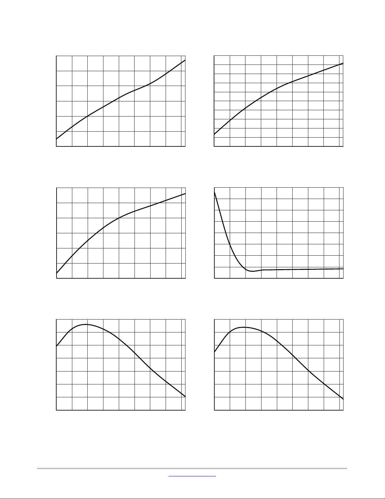
Frequency Foldback
The reduction of no−load standby power associated with
the need for improving the efficiency, requires to change the
traditional fixed−frequency type of operation. This device
implements a switching frequency foldback when the
COMP current passes above a certain level, I
COMPfold
around 68 mA. At this point, the oscillator enters frequency
foldback and reduces its switching frequency.
The internal peak current set−point is following the
COMP current information until its level reaches I
110
100
90
80
70
60
50
40
Frequency [kHz]
30
20
10
, set
Freeze
Below this value, the peak current setpoint is frozen to 30%
of the I
. The only way to further reduce the transmitted
PK(0)
power is to diminish the operating frequency down to F
(25 kHz typically). This value is reached at a COMP current
level of I
COMPfold(end)
(100 mA typically). Below this point,
if the output power continues to decrease, the part enters skip
cycle for the best noise−free performance in no−load
conditions. Figure 37 and Figure 38 depict the adopted
scheme for the part.
.
NCP106x 60 kHz
NCP106x 100 kHz
min
50 60 70 80 90 100
I
[mA]
COMP
Figure 37. By Observing the Current on the COMP Pin, the Controller Reduces
its Switching Frequency for an Improved Performance at Light Load
900
800
NCP1060
NCP1063
700
600
500
400
300
200
Current set point [mA]
100
0
40 50 60 70 80 90 100 110
I
[mA]
COMP
Figure 38. Ipk Set−point is Frozen at Lower Power Demand
www.onsemi.com
21
Page 22

NCP1060, NCP1063
350
300
250
200
150
100
Current set point [mA]
50
0
40 50 60 70 80 90 100 110
I
[mA]
COMP
NCP1060
NCP1063
Figure 39. Ipk Set−point is Frozen at Lower Power Demand (I
Feedback and Skip
Figure 40 depicts the relationship between COMP pin
voltage and current. The COMP pin operates linearly as the
absolute value of COMP current (I
) is above 40 mA. In
COMP
3.5
3.0
2.5
2.0
[V]
COMP
1.5
V
1.0
0.5
0.0
-180 -160 -140 -120 -100 -80 -60 -40 -20 0
≥ 285 mA)
LMOP
this linear operating range, the dynamic resistance is
17.7 kW typically (R
COMP(up)
voltage is 2.7 V typically (V
) and the effective pull up
COMP(REF)
). When I
decreases, the COMP voltage will increase to 3.2 V.
I
[μA]
COMP
COMP
is
Figure 40. COMP Pin Voltage vs. Current
Figure 41 depicts the skip mode block diagram. When the
COMP current information reaches I
COMPskip
, the internal
clock setting the flip−flop is blanked and the internal
consumption of the controller is decreased. The hysteresis of
www.onsemi.com
internal skip comparator is minimized to lower the ripple of
the auxiliary voltage for VCC pin and V
during skip mode. It easies the design of V
of power supply
OUT
over load
CC
range.
22
Page 23

Jittering
NCP1060, NCP1063
OSC
R
COMP(UP)
COMP
Ilimit and OPP Function
V
COMP(REF)
Foldback
I
COMPskip
Figure 41. Skip Cycle Schematic
SKIP
S
Q
Q
R
CS comparator
DRV stage
The function makes the integrated circuit more flexible. The current drawn out of LIM/OPP pin defines the current set point.
900
NCP1060
800
700
NCP1063
600
500
400
300
200
Current set point [mA]
100
0
0 50 100 150 200 250 300 350
Figure 42. Ipk Set−point Dependence on I
There are several known ways to implement Over Power
Protection (OPP), all suffering from particular problems.
These problems range from the added consumption burden
on the converter or the skip−cycle disturbance brought by
the current−sense offset. A way to reduce the power
capability at high line is to capitalize on the negative voltage
swing present on the auxiliary diode anode. During the
power switch on−time, this point dips to –NV
, N being the
in
turns ratio between the primary winding and the auxiliary
winding. The negative plateau on auxiliary winding will
have an amplitude dependant on the input voltage. Resistors
I
[mA]
LMOP
Current
LMOP
R
OPPU
and R
(Figure 43) define current drawn from
OPPL
LIM/OPP and the negative voltage on auxiliary winding.
The negative voltage is tied up with bulk voltage, so the
higher the bulk voltage is, the deeper is the negative voltage
on auxiliary winding, the higher current is drawn from
LIM/OPP pin and the lower the peak current is. During the
internal MOSFET off period, voltage on auxiliary winding
is positive, but the IC ignores the LIM/OPP current. The
positive LIM/OPP current has no influence on proper IC
function.
www.onsemi.com
23
Page 24

NCP1060, NCP1063
VCC
D4
I
COMP
I
LMOP
Aux
winding
I
0
I
COMP
LMDEC
C2
R
OPPU
LIM/OPP
R
OPPL
Figure 43. The OPP Circuitry Affects the Maximum Peak Current Set Point
Ramp Compensation and Ipk Set−point
In order to allow the NCP106X to operate in CCM with a
duty cycle above 50%, a fixed slope compensation is
internally applied to the current−mode control.
Here we got a table of the ramp compensation, the initial
current set point, and the final current set−point of different
versions of switcher.
to CS setpoint
mA
25
250
OSC
S
MOSFET
Q
I
LMDEC
R
I
mA
I
LMOP
IPKL
FreezeIpk(0)
Vramp + Vsense
NCP1060 NCP1063
f
sw
S
I
pk(Duty
=50%)
I
pk(0)
a
60 kHz 100 kHz 60 kHz 100 kHz
8.4 mA/ms 14 mA/ms 15.6 mA/ms 26 mA/ms
250 mA 650 mA
300 mA 780 mA
Figure 44 depicts the variation of IPK set−point vs. the
power switcher duty ratio, which is caused by the internal
ramp compensation.
900
800
700
NCP1060
NCP1063
600
500
400
300
Ipk set-point [mA]
200
100
0
0% 10% 20% 30% 40% 50% 60% 70%
Dutty Ratio [%]
Figure 44. IPK Set−point Varies with Power Switch on Time, which is Caused by the Ramp Compensation
FB Pin Function
The FB pin is used in non isolated SMPS application only.
Portion of the output voltage is connected into the pin. The
voltage is compared with internal V
(3.3 V) using
REF
Operation Transconductance Amplifier (Figure 45). The
OTAs output is connected to COMP pin. The OTA output is
accessible through the COMP pin and is used for the loop
compensation, usually an RC network. The current
capability of OTA is limited to −150 mA typically. The
positive current is defined by internal R
and V
COMP(ref)
voltage. If FB path loop is broken (i.e. the FB
pin is disconnected), an internal current I
pull up the FB pin and the IC stops switching to avoid
uncontrolled output voltage increasing.
In isolated topology, the FB pin should be connected to
GND pin. In this configuration no current flows from OTA
to COMP pin (OTA is disabled) so the OTA has no influence
on regulation at all.
COMP(up)
(1 mA typ.) will
FB
resistor
www.onsemi.com
24
Page 25

NCP1060, NCP1063
V
COMP (REF )
R
COMP (up)
I
COMP
COMP
I
FB
OTA out = 0 A
if FB = 0 V
FB
OTA
V
REF
Figure 45. FB Pin Connection
Design Procedure
The design of an SMPS around a monolithic device does
not differ from that of a standard circuit using a controller
and a MOSFET. However, one needs to be aware of certain
characteristics specific of monolithic devices. Let us follow
the steps:
V
min = 90 Vac or 127 Vdc once rectified, assuming a low
in
bulk ripple
I
OTAlim
V
max = 265 Vac or 375 Vdc
in
V
= 12 V
out
= 5 W
P
out
Operating mode is CCM
η = 0.8
1. The lateral MOSFET body−diode shall never be
forward biased, either during start−up (because of
a large leakage inductance) or in normal operation
as shown in Figure 46. This condition sets the
maximum voltage that can be reflected during toff.
As a result, the Flyback voltage which is reflected
on the drain at the switch opening cannot be larger
than the input voltage. When selecting
components, you thus must adopt a turn ratio
which adheres to the following equation:
N @ǒV
out
) V
Ǔ
f
t V
in,min
2. In our case, since we operate from a 127 V DC rail
while delivering 12 V, we can select a reflected
voltage of 120 V dc maximum. Therefore, the turn
ratio Np:Ns must be smaller than
V
reflect
V
) V
out
+
f
120
12 ) 0.5
+ 9.6orNp:Nst 9.6.
Here we choose N = 8 in this case. We will see later
on how it affects the calculation.
(eq. 2)
350
250
150
50.0
−50.0
1.004M 1.011M 1.018M 1.025M 1.032M
> 0 !!
Figure 46. The Drain−source Wave Shall always be Positive
www.onsemi.com
25
Page 26

Figure 47. Primary Inductance Current
Evolution in CCM
3. Lateral MOSFETs have a poorly doped
body−diode which naturally limits their ability to
sustain the avalanche. A traditional RCD clamping
network shall thus be installed to protect the
MOSFET. In some low power applications, a
simple capacitor can also be used since
V
drain,max
+ Vin) N @ǒV
where L
is the leakage inductance, C
f
out
) V
Ǔ
) I
f
peak
@
Ǹ
capacitance at the drain node (which is increased by
the capacitor you will wire between drain and
source), N the N
voltage, V
finally, I
the secondary diode forward drop and
f
the maximum peak current. Worse case
peak
turn ratio, V
P:NS
out
occurs when the SMPS is very close to regulation,
e.g. the V
target is almost reached and I
out
pushed to the maximum. For this design, we have
selected our maximum voltage around 650 V (at V
= 375 Vdc). This voltage is given by the RCD clamp
installed from the drain to the bulk voltage. We will
see how to calculate it later on.
4. Calculate the maximum operating duty−cycle for
this flyback converter operated in CCM:
d
max
+
+
N @ǒV
1 )
N @ǒV
out
1
V
in,min
N@(V
@ V
out
out
@ V
Ǔ
f
@Vf)
) V
Ǔ
f
in,min
+ 0.44
5. To obtain the primary inductance, we have the
choice between two equations:
Vin@ d
2
Ǔ
in
L +
ǒ
fsw@ K @ P
NCP1060, NCP1063
and defines the amount of ripple we want in CCM (see
Figure 47).
• Small K: deep CCM, implying a large primary
inductance, a low bandwidth and a large leakage
inductance.
• Large K: approaching DCM where the RMS losses are
worse, but smaller inductance, leading to a better
leakage inductance.
From Equation 6, a K factor of 1 (50% ripple), gives an
inductance of:
L +
DI
+
L
The peak current can be evaluated to be:
I
peak
On IL, I
I
Lavg
L
f
(eq. 3)
C
tot
the total
tot
the output
is still
peak
(eq. 4)
(eq. 5)
in
6. Based on the above numbers, we can now evaluate
I
d,rms
7. Off−time and on−time switching losses can be
Where, assume the V
voltage.
DI
where K +
(
127 @ 0.44
60k @ 1 @ 5
Vin@ d
L @ f
sw
I
avg
+
d
can also be calculated:
Lavg
+ I
peak
L
I
Lavg
2
)
+ 10.04 mH
127 @ 0.44
+
10.04m @ 60k
DI
L
)
+
2
DI
L
*
+ 158m *
2
49.2 m
0.44
+ 92.8 mA peak to peak
92.8 m
)
92.8m
+ 158 mA
2
+ 111.6 mA
2
the conduction losses:
2
DI
+ d @ǒI
Ǹ
+ 0.44 @ǒ0.1582* 0.158 @ 0.0928 )
Ǹ
+ 57 mA
peak
2
* I
peak
@ DIL)
If we take the maximum R
L
3
for a 125°C
DS(on)
Ǔ
0.0928
3
2
junction temperature, i.e. 34 W, then conduction
losses worse case are:
P
cond
+ I
d,rms
2
@ R
DS(on)
+ 110 mW
estimated based on the following calculations:
I
@ǒV
P
peak
+
off
0.158 @(127 ) 100 @ 2)@ 10n
+
+ 15.5 mW
) V
bulk
2T
2 @ 16.7 m
is equal to 2 times of reflected
clamp
SW
clamp
Ǔ
@ t
off
(eq. 6)
Ǔ
www.onsemi.com
26
Page 27

NCP1060, NCP1063
I
@ǒV
Pon+
valley
0.0464 @ (127 ) 100) @ 10 n
+
+ 2.1 mW
) N @ (V
bulk
6 @ T
6 @ 16.7 m
SW
) Vf)Ǔ@ t
out
on
(eq. 7)
It is noted that the overlap of voltage and current seen on
MOSFET during turning on and off duration is dependent on
the snubber and parasitic capacitance seen from drain pin.
Therefore the t
and ton in Equation 7 and Equation 8 have
off
to be modified after measuring on the bench.
8. The theoretical total power is then
117 + 15.5 + 2.1 = 127.6 mW
9. If the NCP106X operates at DSS mode, then the
losses caused by DSS mode should be counted as
losses of this device on the following calculation:
P
+ I
DSS
MOSFET Protection
CC1
@ V
+ 0.8m @ 375 + 300 mW
in.max
(eq. 8)
As in any Flyback design, it is important to limit the drain
excursion to a safe value, e.g. below the MOSFET BVdss
which is 700 V. Figure 48 a−b−c present possible
implementations:
Figure 48. a, b, c : Different Options to Clamp the Leakage Spike
Figure 48a: the simple capacitor limits the voltage
according to the lateral MOSFET body−diode shall never be
forward biased, either during start−up (because of a large
leakage inductance) or in normal operation as shown by
Figure 46. This condition sets the maximum voltage that can
be reflected during t
. As a result, the flyback voltage
off
which is reflected on the drain at the switch opening cannot
be larger than the input voltage. When selecting
components, you must adopt a turn ratio which adheres to
the following Equation 3. This option is only valid for low
power applications, e.g. below 5 W, otherwise chances exist
to destroy the MOSFET. After evaluating the leakage
inductance, you can compute C with (Equation 4). Typical
values are between 100 pF and up to 470 pF. Large
capacitors increase capacitive losses...
Figure 48b: the most standard circuitry is called the RCD
network. You calculate R
clamp
and C
clamp
using the
following formulae:
R
+
clamp
C
+
clamp
V
is usually selected 50−80 V above the reflected
clamp
value N x (V
2 @ V
V
ripple
+ Vf). The diode needs to be a fast one and
out
@ǒV
clamp
L
V
clamp
@ fsw@ R
leak
clamp
@ I
clamp
) N @ (V
2
@ f
leak
out
sw
) Vf)
Ǔ
(eq. 9)
a MUR160 represents a good choice. One major drawback
of the RCD network lies in its dependency upon the peak
current. Worse case occurs when I
and V
is close to reach the steady−state value.
out
and Vin are maximum
peak
Figure 48c: this option is probably the most expensive of
all three but it offers the best protection degree. If you need
a very precise clamping level, you must implement a zener
diode or a TVS. There are little technology differences
behind a standard zener diode and a TVS. However, the die
area is far bigger for a transient suppressor than that of zener.
A 5 W zener diode like the 1N5388B will accept 180 W peak
power if it lasts less than 8.3 ms. If the peak current in the
worse case (e.g. when the PWM circuit maximum current
limit works) multiplied by the nominal zener voltage
exceeds these 180 W, then the diode will be destroyed when
the supply experiences overloads. A transient suppressor
like the P6KE200 still dissipates 5 W of continuous power
but is able to accept surges up to 600 W @ 1 ms. Select the
zener or TVS clamping level between 40 to 80 volts above the
reflected output voltage when the supply is heavily loaded.
As a good design practice, it is recommended to
implement one of this protection to make sure Drain pin
voltage doesn’t go above 650 V (to have some margin
between Drain pin voltage and BVdss) during most stringent
operating conditions (high Vin and peak power).
www.onsemi.com
27
Page 28

NCP1060, NCP1063
Power Dissipation and Heatsinking
The NCP106X welcomes two dissipating terms, the DSS
current−source (when active) and the MOSFET. Thus, P
= P
DSS
+ P
MOSFET
. It is mandatory to properly manage the
heat generated by losses. If no precaution is taken, risks exist
to trigger the internal thermal shutdown (TSD). To help
dissipating the heat, the PCB designer must foresee large
copper areas around the package. Take the PDIP−7 package
as an example, when surrounded by a surface approximately
200 mm2 of 35 mm copper, the maximum power the device
can thus evacuate is:
tot
T
* T
+
Jmax
P
max
R
qJA
ambmax
(eq. 10)
which gives around 870 mW for an ambient of 50°C and a
maximum junction of 150°C. If the surface is not large
enough, the R
is growing and the maximum power the
JA
θ
device can evacuate decreases. Figure 49 gives a possible
layout to help drop the thermal resistance.
Figure 49. A Possible PCB Arrangement to Reduce the Thermal Resistance Junction−to−Ambient
Bill of material:
C1 Bulk capacitor, input DC voltage is connected to the capacitor
C2, R1, D1 Clamping elements
C3 Vcc capacitor
OK1 Optocoupler
R2 Resistor to setting I
Table 6. ORDERING INFORMATION
Device Frequency R
NCP1060AP060G 60 kHz 34 Yes
NCP1060AP100G 100 kHz 34 Yes 50 Units / Rail
NCP1060AD060R2G 60 kHz 34 Ye s
NCP1060AD100R2G 100 kHz 34 Yes 2500 / Tape & Reel
NCP1060BD060R2G 60 kHz 34 No 2500 / Tape & Reel
NCP1060BD100R2G 100 kHz 34 No 2500 / Tape & Reel
NCP1063AP060G 60 kHz 11.4 Ye s
NCP1063AP100G 100 kHz 11.4 Yes 50 Units / Rail
NCP1063AD060R2G 60 kHz 11.4 Ye s
NCP1063AD100R2G 100 kHz 11.4 Ye s 2500 / Tape & Reel
†For information on tape and reel specifications, including part orientation and tape sizes, please refer to our Tape and Reel Packaging
Specifications Brochure, BRD8011/D.
PEAK
current
DS(on)
Brown In Package Type Shipping
PDIP−7
(Pb−Free)
SOIC−10
(Pb−Free)
PDIP−7
(Pb−Free)
SOIC−16
(Pb−Free)
50 Units / Rail
2500 / Tape & Reel
50 Units / Rail
2500 / Tape & Reel
†
www.onsemi.com
28
Page 29

MECHANICAL CASE OUTLINE
PACKAGE DIMENSIONS
PDIP−7 (PDIP−8 LESS PIN 6)
SCALE 1:1
D
14
NOTE 8
TOP VIEW
e/2
A1
D1
e
SIDE VIEW
A
58
H
E1
b2
B
A2
A
NOTE 3
L
SEATING
PLANE
C
8X
b
M
0.010 CA
MBM
CASE 626A
ISSUE C
E
END VIEW
WITH LEADS CONSTRAINED
NOTE 5
M
eB
END VIEW
NOTE 6
DATE 22 APR 2015
NOTES:
1. DIMENSIONING AND TOLERANCING PER ASME Y14.5M, 1994.
2. CONTROLLING DIMENSION: INCHES.
3. DIMENSIONS A, A1 AND L ARE MEASURED WITH THE PACKAGE SEATED IN JEDEC SEATING PLANE GAUGE GS−3.
4. DIMENSIONS D, D1 AND E1 DO NOT INCLUDE MOLD FLASH
OR PROTRUSIONS. MOLD FLASH OR PROTRUSIONS ARE
NOT TO EXCEED 0.10 INCH.
5. DIMENSION E IS MEASURED AT A POINT 0.015 BELOW DATUM
PLANE H WITH THE LEADS CONSTRAINED PERPENDICULAR
TO DATUM C.
6. DIMENSION eB IS MEASURED AT THE LEAD TIPS WITH THE
LEADS UNCONSTRAINED.
c
7. DATUM PLANE H IS COINCIDENT WITH THE BOTTOM OF THE
LEADS, WHERE THE LEADS EXIT THE BODY.
8. PACKAGE CONTOUR IS OPTIONAL (ROUNDED OR SQUARE
CORNERS).
INCHES
DIM MIN MAX
A −−−− 0.210
A1 0.015 −−−−
A2 0.115 0.195 2.92 4.95
b 0.014 0.022
b2
0.060 TYP 1.52 TYP
C 0.008 0.014
D 0.355 0.400
D1 0.005 −−−−
E 0.300 0.325
E1 0.240 0.280 6.10 7.11
e 0.100 BSC
eB −−−− 0.430 −−− 10.92
L 0.115 0.150 2.92 3.81
M −−−− 10
MILLIMETERS
MIN MAX
−−− 5.33
0.38 −−−
0.35 0.56
0.20 0.36
9.02 10.16
0.13 −−−
7.62 8.26
2.54 BSC
−−− 10
°°
GENERIC
MARKING DIAGRAM*
XXXXXXXXX
AWL
YYWWG
XXXX = Specific Device Code
A = Assembly Location
WL = Wafer Lot
YY = Year
WW = Work Week
G = Pb−Free Package
*This information is generic. Please refer to
device data sheet for actual part marking.
Pb−Free indicator, “G” or microdot “ G”,
may or may not be present.
DOCUMENT NUMBER:
DESCRIPTION:
ON Semiconductor and are trademarks of Semiconductor Components Industries, LLC dba ON Semiconductor or its subsidiaries in the United States and/or other countries.
ON Semiconductor reserves the right to make changes without further notice to any products herein. ON Semiconductor makes no warranty, representation or guarantee regarding
the suitability of its products for any particular purpose, nor does ON Semiconductor assume any liability arising out of the application or use of any product or circuit, and specifically
disclaims any and all liability, including without limitation special, consequential or incidental damages. ON Semiconductor does not convey any license under its patent rights nor the
rights of others.
98AON11774D
PDIP−7 (PDIP−8 LESS PIN 6)
Electronic versions are uncontrolled except when accessed directly from the Document Repository.
Printed versions are uncontrolled except when stamped “CONTROLLED COPY” in red.
PAGE 1 OF 1
© Semiconductor Components Industries, LLC, 2019
www.onsemi.com
Page 30

MECHANICAL CASE OUTLINE
PACKAGE DIMENSIONS
SCALE 1:1
−A−
16 9
−B−
18
G
K
C
−T−
SEATING
PLANE
D
16 PL
0.25 (0.010) A
M
S
B
T
S
CASE 751B−05
8 PLP
0.25 (0.010) B
SOIC−16
ISSUE K
M
DATE 29 DEC 2006
NOTES:
1. DIMENSIONING AND TOLERANCING PER ANSI
Y14.5M, 1982.
2. CONTROLLING DIMENSION: MILLIMETER.
3. DIMENSIONS A AND B DO NOT INCLUDE MOLD
PROTRUSION.
4. MAXIMUM MOLD PROTRUSION 0.15 (0.006) PER SIDE.
5. DIMENSION D DOES NOT INCLUDE DAMBAR
M
S
X 45
R
_
F
J
PROTRUSION. ALLOWABLE DAMBAR PROTRUSION
SHALL BE 0.127 (0.005) TOTAL IN EXCESS OF THE D
DIMENSION AT MAXIMUM MATERIAL CONDITION.
DIM MIN MAX MIN MAX
A 9.80 10.00 0.386 0.393
B 3.80 4.00 0.150 0.157
C 1.35 1.75 0.054 0.068
D 0.35 0.49 0.014 0.019
F 0.40 1.25 0.016 0.049
G 1.27 BSC 0.050 BSC
J 0.19 0.25 0.008 0.009
K 0.10 0.25 0.004 0.009
M 0 7 0 7
____
P 5.80 6.20 0.229 0.244
R 0.25 0.50 0.010 0.019
INCHESMILLIMETERS
STYLE 1:
PIN 1. COLLECTOR
2. BASE
3. EMITTER
4. NO CONNECTION
5. EMITTER
6. BASE
7. COLLECTOR
8. COLLECTOR
9. BASE
10. EMITTER
11. NO CONNECTION
12. EMITTER
13. BASE
14. COLLECTOR
15. EMITTER
16. COLLECTOR
STYLE 5:
PIN 1. DRAIN, DYE #1
2. DRAIN, #1
3. DRAIN, #2
4. DRAIN, #2
5. DRAIN, #3
6. DRAIN, #3
7. DRAIN, #4
8. DRAIN, #4
9. GATE, #4
10. SOURCE, #4
11. GATE, #3
12. SOURCE, #3
13. GATE, #2
14. SOURCE, #2
15. GATE, #1
16. SOURCE, #1
STYLE 2:
PIN 1. CATHODE
2. ANODE
3. NO CONNECTION
4. CATHODE
5. CATHODE
6. NO CONNECTION
7. ANODE
8. CATHODE
9. CATHODE
10. ANODE
11. NO CONNECTION
12. CATHODE
13. CATHODE
14. NO CONNECTION
15. ANODE
16. CATHODE
STYLE 6:
PIN 1. CATHODE
2. CATHODE
3. CATHODE
4. CATHODE
5. CATHODE
6. CATHODE
7. CATHODE
8. CATHODE
9. ANODE
10. ANODE
11. ANODE
12. ANODE
13. ANODE
14. ANODE
15. ANODE
16. ANODE
STYLE 3:
PIN 1. COLLECTOR, DYE #1
2. BASE, #1
3. EMITTER, #1
4. COLLECTOR, #1
5. COLLECTOR, #2
6. BASE, #2
7. EMITTER, #2
8. COLLECTOR, #2
9. COLLECTOR, #3
10. BASE, #3
11. EMITTER, #3
12. COLLECTOR, #3
13. COLLECTOR, #4
14. BASE, #4
15. EMITTER, #4
16. COLLECTOR, #4
STYLE 7:
PIN 1. SOURCE N‐CH
2. COMMON DRAIN (OUTPUT)
3. COMMON DRAIN (OUTPUT)
4. GATE P‐CH
5. COMMON DRAIN (OUTPUT)
6. COMMON DRAIN (OUTPUT)
7. COMMON DRAIN (OUTPUT)
8. SOURCE P‐CH
9. SOURCE P‐CH
10. COMMON DRAIN (OUTPUT)
11. COMMON DRAIN (OUTPUT)
12. COMMON DRAIN (OUTPUT)
13. GATE N‐CH
14. COMMON DRAIN (OUTPUT)
15. COMMON DRAIN (OUTPUT)
16. SOURCE N‐CH
STYLE 4:
PIN 1. COLLECTOR, DYE #1
2. COLLECTOR, #1
3. COLLECTOR, #2
4. COLLECTOR, #2
5. COLLECTOR, #3
6. COLLECTOR, #3
7. COLLECTOR, #4
8. COLLECTOR, #4
9. BASE, #4
10. EMITTER, #4
11. BASE, #3
12. EMITTER, #3
13. BASE, #2
14. EMITTER, #2
15. BASE, #1
16. EMITTER, #1
SOLDERING FOOTPRINT
1
16X
0.58
89
8X
6.40
16X
1.12
16
DIMENSIONS: MILLIMETERS
1.27
PITCH
DOCUMENT NUMBER:
DESCRIPTION:
ON Semiconductor and are trademarks of Semiconductor Components Industries, LLC dba ON Semiconductor or its subsidiaries in the United States and/or other countries.
ON Semiconductor reserves the right to make changes without further notice to any products herein. ON Semiconductor makes no warranty, representation or guarantee regarding
the suitability of its products for any particular purpose, nor does ON Semiconductor assume any liability arising out of the application or use of any product or circuit, and specifically
disclaims any and all liability, including without limitation special, consequential or incidental damages. ON Semiconductor does not convey any license under its patent rights nor the
rights of others.
© Semiconductor Components Industries, LLC, 2019
98ASB42566B
SOIC−16
Electronic versions are uncontrolled except when accessed directly from the Document Repository.
Printed versions are uncontrolled except when stamped “CONTROLLED COPY” in red.
PAGE 1 OF 1
www.onsemi.com
Page 31

MECHANICAL CASE OUTLINE
PACKAGE DIMENSIONS
10
1
SCALE 1:1
2X 5 TIPS
D
D
H
1
C0.20
B
TOP VIEW
C0.10
A
A1
SIDE VIEW
RECOMMENDED
SOLDERING FOOTPRINT*
10X
0.58
2X
C0.10 A-B
A
2X
C0.10 A-B
610
E
5
b10X
M
0.25
10X
C
C0.10
e
C
1.00
PITCH
SEATING
PLANE
L2
A-B D
DETAIL A
SOIC−10 NB
CASE 751BQ
ISSUE B
F
h
X 45
A3
L
DETAIL A
_
END VIEW
C
SEATING
PLANE
M
DATE 26 NOV 2013
NOTES:
1. DIMENSIONING AND TOLERANCING PER
ASME Y14.5M, 1994.
2. CONTROLLING DIMENSION: MILLIMETERS.
3. DIMENSION b DOES NOT INCLUDE DAMBAR
PROTRUSION. ALLOWABLE PROTRUSION
SHALL BE 0.10mm TOTAL IN EXCESS OF ’b’
AT MAXIMUM MATERIAL CONDITION.
4. DIMENSIONS D AND E DO NOT INCLUDE
MOLD FLASH, PROTRUSIONS, OR GATE
BURRS. MOLD FLASH, PROTRUSIONS, OR
GATE BURRS SHALL NOT EXCEED 0.15mm
PER SIDE. DIMENSIONS D AND E ARE DETERMINED AT DATUM F.
5. DIMENSIONS A AND B ARE TO BE DETERMINED AT DATUM F.
6. A1 IS DEFINED AS THE VERTICAL DISTANCE
FROM THE SEATING PLANE TO THE LOWEST
POINT ON THE PACKAGE BODY.
MILLIMETERS
DIMDMIN MAX
A 1.25 1.75
A1 0.10 0.25
A3 0.17 0.25
b 0.31 0.51
4.80 5.00
E 3.80 4.00
e 1.00 BSC
H 5.80 6.20
h 0.37 REF
L 0.40 0.80
L2 0.25 BSC
M 0 8
__
GENERIC
MARKING DIAGRAM*
10
XXXXX
ALYWX
G
1
6.50
XXXXX = Specific Device Code
A = Assembly Location
L = Wafer Lot
Y = Year
W = Work Week
10X
1.18
1
DIMENSION: MILLIMETERS
*For additional information on our Pb−Free strategy and soldering
details, please download the ON Semiconductor Soldering and
Mounting Techniques Reference Manual, SOLDERRM/D.
DOCUMENT NUMBER:
DESCRIPTION:
ON Semiconductor and are trademarks of Semiconductor Components Industries, LLC dba ON Semiconductor or its subsidiaries in the United States and/or other countries.
ON Semiconductor reserves the right to make changes without further notice to any products herein. ON Semiconductor makes no warranty, representation or guarantee regarding
the suitability of its products for any particular purpose, nor does ON Semiconductor assume any liability arising out of the application or use of any product or circuit, and specifically
disclaims any and all liability, including without limitation special, consequential or incidental damages. ON Semiconductor does not convey any license under its patent rights nor the
rights of others.
98AON52341E
SOIC−10 NB
Electronic versions are uncontrolled except when accessed directly from the Document Repository.
Printed versions are uncontrolled except when stamped “CONTROLLED COPY” in red.
G = Pb−Free Package
*This information is generic. Please refer
to device data sheet for actual part
marking. Pb−Free indicator, “G”, may
or not be present.
PAGE 1 OF 1
© Semiconductor Components Industries, LLC, 2019
www.onsemi.com
Page 32

ON Semiconductor and are trademarks of Semiconductor Components Industries, LLC dba ON Semiconductor or its subsidiaries in the United States and/or other countries.
ON Semiconductor owns the rights to a number of patents, trademarks, copyrights, trade secrets, and other intellectual property. A listing of ON Semiconductor ’s product/patent
coverage may be accessed at www.onsemi.com/site/pdf/Patent−Marking.pdf
ON Semiconductor makes no warranty, representation or guarantee regarding the suitability of its products for any particular purpose, nor does ON Semiconductor assume any liability
arising out of the application or use of any product or circuit, and specifically disclaims any and all liability, including without limitation special, consequential or incidental damages.
Buyer is responsible for its products and applications using ON Semiconductor products, including compliance with all laws, regulations and safety requirements or standards,
regardless of any support or applications information provided by ON Semiconductor. “Typical” parameters which may be provided in ON Semiconductor data sheets and/or
specifications can and do vary in different applications and actual performance may vary over time. All operating parameters, including “Typicals” must be validated for each customer
application by customer’s technical experts. ON Semiconductor does not convey any license under its patent rights nor the rights of others. ON Semiconductor products are not
designed, intended, or authorized for use as a critical component in life support systems or any FDA Class 3 medical devices or medical devices with a same or similar classification
in a foreign jurisdiction or any devices intended for implantation in the human body. Should Buyer purchase or use ON Semiconductor products for any such unintended or unauthorized
application, Buyer shall indemnify and hold ON Semiconductor and its officers, employees, subsidiaries, affiliates, and distributors harmless against all claims, costs, damages, and
expenses, and reasonable attorney fees arising out of, directly or indirectly, any claim of personal injury or death associated with such unintended or unauthorized use, even if such
claim alleges that ON Semiconductor was negligent regarding the design or manufacture of the part. ON Semiconductor is an Equal Opportunity/Affirmative Action Employer. This
literature is subject to all applicable copyright laws and is not for resale in any manner.
. ON Semiconductor reserves the right to make changes without further notice to any products herein.
PUBLICATION ORDERING INFORMATION
LITERATURE FULFILLMENT:
Email Requests to: orderlit@onsemi.com
ON Semiconductor Website: www.onsemi.com
TECHNICAL SUPPORT
North American Technical Support:
Voice Mail: 1 800−282−9855 Toll Free USA/Canada
Phone: 011 421 33 790 2910
Europe, Middle East and Africa Technical Support:
Phone: 00421 33 790 2910
For additional information, please contact your local Sales Representative
◊
www.onsemi.com
1
 Loading...