

Page 1
NCN8024GEVB Series
www.BDTIC.com/ON/
NCN8024
SOIC-28 & TSSOP-28
Evaluation Board
User's Manual
Introduction
This document gives a detailed description of the
NCN8024 Evaluation Boards (SOIC−28 & TSSOP−28
versions) with the Bill Of Material (BOM), board schematic
and layout. The appropriate lab test setup is also provided.
The NCN8024 Evaluation Boards have been designed to
help for a quick evaluation of the NCN8024 Smart card
interface device.
This document has to be used with the NCN8024
datasheet. The datasheet contains full technical details
http://onsemi.com
EVAL BOARD USER’S MANUAL
regarding the NCN8024 specifications and operation. The
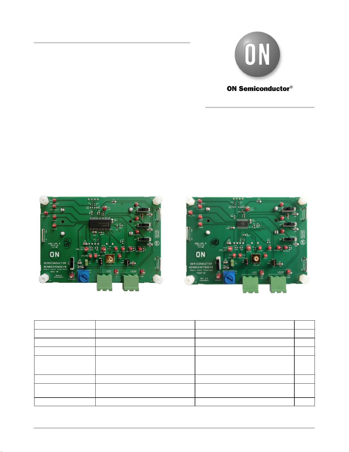
board (FR4 material) is implemented in two metal layers.
The top and Bottom layers have thicknesses of 35 mm. The
PCB thickness is 1.6 mm with dimensions of 100 mm by
74 mm (see Figure 1).
These evaluation boards can be used to evaluate the device
performance.
Figure 1. Evaluation Boards − SOIC−28 & TSSOP−28
Table 1. EQUIPMENT
Description Main Features Example of Equipment (Note 1) Qty
Regulated Power Supply 200 mA DC Current Capability Tektronix PS2520G 2
Multimeter Keitley 2000 or 2001 2
Sourcemeter Keitley 2400 1
Oscilloscope 500 MHz Bandwidth, Four Channel Scope,
Voltage Probe 4 Probes 500 MHz Bandwidth Tektronix or Lecroy 4
Waveform Generator Pattern Genarator Agilent 81104A 80 MHz or HP8110A
SMB Cable External Clock Input 1
1. Equipment used in the context of this Application Note Manual.
2. Greater Scope memory per channel offers better resolution.
Semiconductor Components Industries, LLC, 2012
June, 2012 − Rev. 0
Min 1 Mbit Memory per Channel (Note 2)
1 Publication Order Number:
Tecktronix TDS744, 754 or 784/TDS5054
Series or Lecroy WR5060 TDS5104B,
1 GHz, 5GS/s
150 MHz 2 Outputs
1
1
EVBUM2127/D
Page 2
NCN8024GEVB Series
www.BDTIC.com/ON/
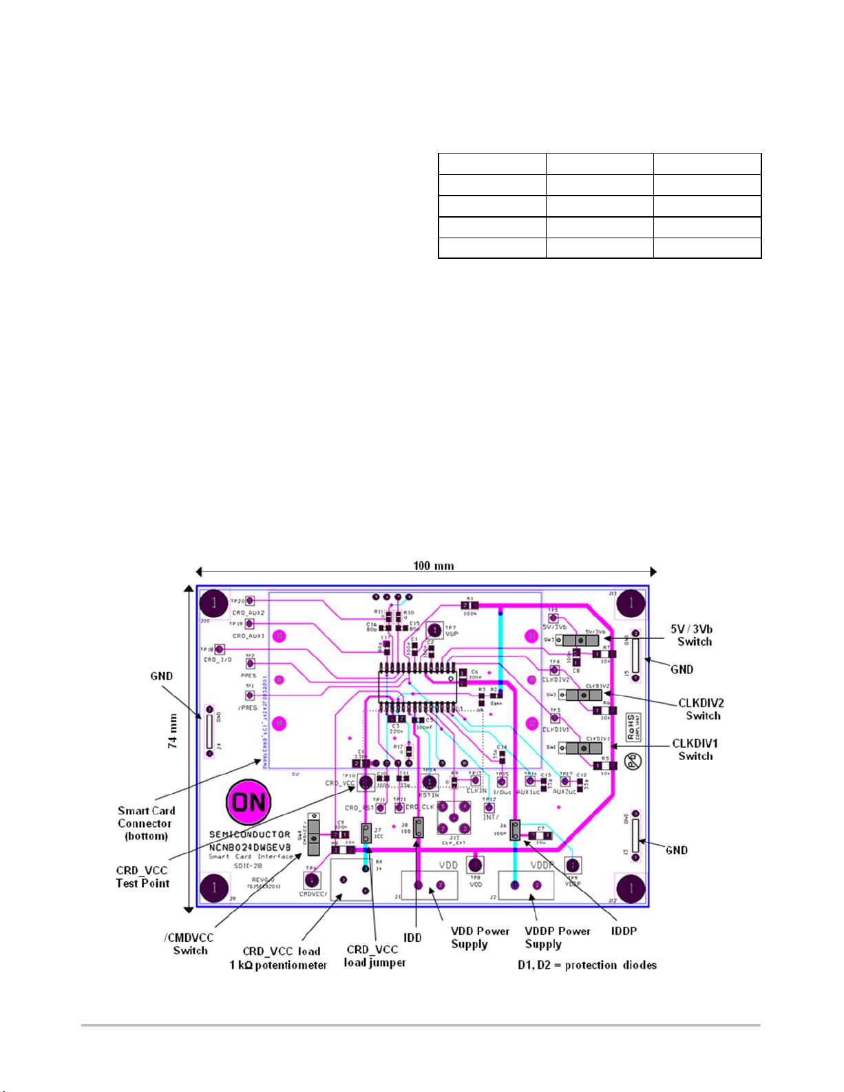
Test Procedure
See Figure 2.
Initial Setups (Figure 2)
The initial setups given here are recommended before
starting measurements on the board.
Set the CMDVCC/in the OFF Position (High)
Set CLKDIV1 and CLKDIV2 into Low Position
(Lowest Frequency Fclkin)
Set 5V/3Vbar into a 5V Position
As a Precaution, Turn the 1 kW Potentiometer to Obtain
a Resistor Output Value of 1 kW, and then Connect the
Jumper
DC Power Supplies
Two power supplies are used to bias the demo board.
V
is the input voltage of the DC-DC converter. VDD is
DDP
the “digital” power supply which biases the input stages of
the NCN8024 device (control and signal inputs).
V
and V
DD
correct operation.
Connect the V
Connector J1
Connect the V
Connector J2
Power up V
Power up V
must be connected to the board for a
DDP
Power Supply Using the 2 Pin Male
DD
Power Supply Using the 2 Pin Male
DDP
in the Range 4.5 V–5.5 V
DDP
in the Range 2.7 V–5.5 V
DD
Clock Frequency
CLKDIV1 and CLKDIV2 select the frequency divider
according to the Table 2.
Table 2. CLOCK FREQUENCY
CLKDIV1 CLKDIV2 Divider
1 0 DIV 1/1
1 1 DIV 1/2
0 1 DIV 1/4
0 0 DIV 1/8
Card Presence
The socket we use is a normally open, so CDR-PRES/ has
been chosen; nevertheless the CRD_PRES and
CRD_PRES/ test points can also be used for signaling the
presence of a card and starting up the circuit.
Start the Measurement
To start the measurements, set the board as it follows:
Set CLKDIV1 and CLKDIV2 to Select the Correct
Frequency
Set 5V/3Vbar to Select the Correct Output Voltage
Jumpers:
1kW Potentiometer Jumper: Not Connected to Start
Measurement
Finally, Toggle/CMDVCC from High to Low to Start
the Device (Activation Sequence Run)
Figure 2. SOIC−28 Board Description (Equivalent for TSSOP−28)
http://onsemi.com
2
Page 3

NCN8024GEVB Series
www.BDTIC.com/ON/
Figure 3. Schematic
http://onsemi.com
3
Page 4

NCN8024GEVB Series
www.BDTIC.com/ON/
Table 3. BILL OF MATERIAL (BOM)
Designator Qty Description Value Footprint Manufacturer Part Number
C1, C2, C5 3
C3 1
C4 1
C6 1
C7 1
C8, C9 2
C10 1 Do Not Populate − SM/C_0603H Do Not Populate Do Not Populate
C11, C12,
C13, C14
C15, C16,
C17
R1 1
R2 1 Do Not Populate − SM/C_0603H Do Not Populate Do Not Populate
R3, R9, R10,
R11, R12
R4 1 Single Turn Cermet
R5, R6, R7,R84
SW1, SW2,
SW3, SW4
TP1-TP5,
TP11-TP13,
TP15-TP21
TP6, TP7,
TP8, TP9,
TP10, TP14
J1, J2 2 VDD, VDDP, 2 Pins,
J3, J4, J5 3 Ground: Strap, Brass,
J6, J7, J8 3 IDD, IDDP, ICC,
J9, J10, J11,
J12
J9, J10, J11,
J12
J13 1 SMB Connector − SMB/V Amphenol Connex 142138
U1 1 NCN8024 Smart Card
U2 1 Smart Card Socket − SmartCard_
CAP CER .1 mF 16 V
10% X7R 0603
CAP CER .22 mF 16 V
X7R 10% 0805
CAP CER .33 mF 16 V
X7R 10% 0805
CAP CER .1 mF 25 V
10% X7R 0805
CAP CER 10 mF 6.3 V
X5R 10% 1206
CAP CER .1 mF 25 V
10% X7R 0805
4 Do Not Populate − SM/C_0603H Do Not Populate Do Not Populate
3 Do Not Populate − SM/C_0603H Do Not Populate Do Not Populate
RES 100 kW 1/4 W 5%
0805 SMD
5
RES 0.0 W 1/10 W 0603
SMD
Trimmer 1 kW, 0.5 W,
10%, 63M100R
RES 10 kW 1/4 W 5%
1206 SMD
4 PCB Slide Switches − INTER3-2,54 EAO 09.03290.01
15 CLKDIV1/2, 5 V/3 Vb,
INT/, I/OUC, AUX1UC,
AUX2UC, CLKIN,
CRD_AUX1, _AUX2,
_I/O, _CLK, _RST,
/PRES, PRES, Clip Test
Point Hole Diameter
1.0 mm
6 /CMDVCC, VUP, VDD,
VDDP, CRD_VCC,
RSTIN, Clip Test Point
Hole Diameter 1.6 mm
Male Connector,
5.08 mm Step
Diameter 1.0 mm, Pitch
10.16 mm, Height
9.9 mm
Breakable Single Row,
Header (2 Pins)
4 Standoff Nut − Standoff Hole Keystone 1903C
4 Standoff Screw − Standoff Hole Keystone 4814K-ND
Interface
100 nF SM/C_0603H Murata GRM188R71C104KA01D
220 nF SM/C_0805H TDK C2012X7R1C224K
330 nF SM/C_0805H TDK C2012X7R1C334K/1.25
100 nF SM/C_0805H Murata GRM21BR71E104KA01L
10 mF
100 nF SM/C_0805H Murata GRM21BR71E104KA01L
100 kW
0 SM/C_0603H Stackpole Electronics Inc RMCF0603ZT0R00
1kW
10 kW
− TP_1 Keystone 5000
− TP_1.6MMHOLE_KEYS
− MSTBA2-5.08MM Phoenix Contact MSTBA2.52G5.08
− GND_STRP HARWIN D3082-46
− CON2-2.54 TYCO Amp 5-826629-0
− SOIC−28/TSSOP−28 ON Semiconductor NCN8024DWR2G/
SM/C_1206H TDK C3216X5R0J106K/1.60
SM/C_0805H Rohm Semiconductor ESR10EZPJ104
CERMET-72PT Bourns 3386F-1-102TLF
SM/C_1206H Rohm Semiconductor MCR18EZPJ103
TONE_5010
FCI_74343L0825S01
Keystone 5010
NCN8024DTBR2G
FCI 7434L0825S01LF
http://onsemi.com
4
Page 5

NCN8024GEVB Series
www.BDTIC.com/ON/
ON Semiconductor and are registered trademarks of Semiconductor Components Industries, LLC (SCILLC). SCILLC owns the rights to a number of patents, trademarks,
copyrights, trade secrets, and other intellectual property. A listing of SCILLC’s product/patent coverage may be accessed at www.onsemi.com/site/pdf/Patent−Marking.pdf. SCILLC
reserves the right to make changes without further notice to any products herein. SCILLC makes no warranty, representation or guarantee regarding the suitability of its products for any
particular purpose, nor does SCILLC assume any liability arising out of the application or use of any product or circuit, and specifically disclaims any and all liability, including without
limitation special, consequential or incidental damages. “Typical” parameters which may be provided in SCILLC data sheets and/or specifications can and do vary in different applications
and actual performance may vary over time. All operating parameters, including “Typicals” must be validated for each customer application by customer’s technical experts. SCILLC
does not convey any license under its patent rights nor the rights of others. SCILLC products are not designed, intended, or authorized for use as components in systems intended for
surgical implant into the body, or other applications intended to support or sustain life, or for any other application in which the failure of the SCILLC product could create a situation where
personal injury or death may occur. Should Buyer purchase or use SCILLC products for any such unintended or unauthorized application, Buyer shall indemnify and hold SCILLC and
its officers, employees, subsidiaries, affiliates, and distributors harmless against all claims, costs, damages, and expenses, and reasonable attorney fees arising out of, directly or indirectly,
any claim of personal injury or death associated with such unintended or unauthorized use, even if such claim alleges that SCILLC was negligent regarding the design or manufacture
of the part. SCILLC is an Equal Opportunity/Affirmative Action Employer. This literature is subject to all applicable copyright laws and is not for resale in any manner.
PUBLICATION ORDERING INFORMATION
LITERATURE FULFILLMENT:
Literature Distribution Center for ON Semiconductor
P.O. Box 5163, Denver, Colorado 80217 USA
Phone: 303−675−2175 or 800−344−3860 Toll Free USA/Canada
Fax: 303−675−2176 or 800−344−3867 Toll Free USA/Canada
Email: orderlit@onsemi.com
N. American Technical Support: 800−282−9855 Toll Free
USA/Canada
Europe, Middle East and Africa Technical Support:
Phone: 421 33 790 2910
Japan Customer Focus Center
Phone: 81−3−5817−1050
http://onsemi.com
5
ON Semiconductor Website: www.onsemi.com
Order Literature: http://www.onsemi.com/orderlit
For additional information, please contact your local
Sales Representative
EVBUM2127/D
 Loading...