

Page 1
© Semiconductor Components Industries, LLC, 2011
December, 2011 − Rev. P0
1 Publication Order Number:
NCN49597/D
NCN49597
Product Preview
Power Line Carrier Modem
ON Semiconductor’s NCN49597 is an IEC 61334−5−1 compliant
power line carrier modem using spread−FSK (S−FSK) modulation for
robust low data rate communication over power lines. NCN49597 is
built around an ARM processor core, and includes the MAC layer.
With this robust modulation technique, signals on the power lines can
pass long distances. The half−duplex operation is automatically
synchronized to the mains, and can be up to 4800 bits/sec.
The product configuration is done via its serial interface, which
allows the user to concentrate on the development of the application.
The NCN49597 is implemented in ON Semiconductor mixed signal
technology, combining both analog circuitry and digital functionality
on the same IC.
Features
• Power Line Carrier Modem for 50 and 60 Hz Mains
• Fully compliant to IEC 61334−5−1 and CENELEC EN 50065−1
• Complete Handling of Protocol Layers Physical to MAC
• Programmable Carrier Frequencies in CENELEC A-Band from 9 to
95 kHz; B−Band from 95 to 125 kHz, in 10 Hz Steps
• Half Duplex
• Data Rate Selectable:
300 – 600 – 1200 − 2400 – 4800 baud (@ 50 Hz)
360 – 720 – 1440 − 2880 – 5760 baud (@ 60 Hz)
• Synchronization on Mains
• Repetition Algorithm Boost the Robustness of Communication
• SCI Port to Application Microcontroller
• SCI Baudrate Selectable: 9.6 – 19.2 – 38.4 − 115.2 kb
• Power Supply 3.3 V
• Ambient Temperature Range: −40°C to +80°C
• These Devices are Pb−Free and are RoHS Compliant*
Typical Applications
• ARM: Automated Remote Meter Reading
• Remote Security Control
• Streetlight Control
• Transmission of Alerts (Fire, Gas Leak, Water Leak)
*For additional information on our Pb−Free strategy and soldering details, please
download the ON Semiconductor Soldering and Mounting Techniques
Reference Manual, SOLDERRM/D.
This document contains information on a product under development. ON Semiconductor
reserves the right to change or discontinue this product without notice.
ON
e3
ARM
See detailed ordering and shipping information in the package
dimensions section on page 27 of this data sheet.
ORDERING INFORMATION
XXXX = Date Code
Y = Plant Identifier
ZZ = Traceability Code
http://onsemi.com
MARKING DIAGRAMS
152
QFN52 8x8, 0.5P
CASE 485M
XXXXYZZ
NCN 49597
C597−901
1
52
Page 2
NCN49597
http://onsemi.com
2
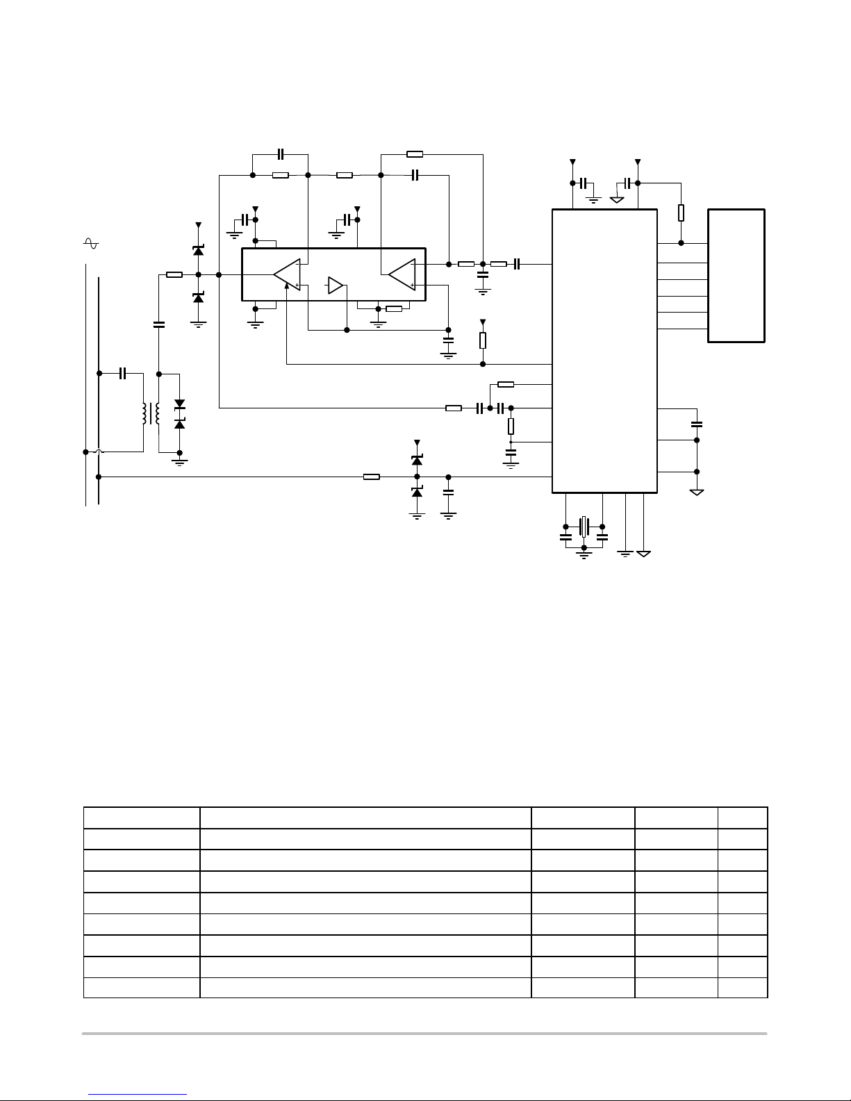
APPLICATION
Application Example
PC20111120 .1
TX_OUT
NCN49597
TX_ENB
ZC_IN
REF_OUT
RX_IN
RX_OUT
XTAL _IN
XTAL_OUT
Appli
&
Metering
mC
TXD
RXD
BR0
BR1
RESB
VSSA
VSS
T_REQ
VDD
VDDA
3V3_A 3V3_D
1:2
C
1
R
1
C
2
R
2
C
DREF
C
16
C
17
3V3_A
D
5
D
1
D
2
D
3
D
4
R
12
C
11
C
12
R
14
C
15
C
14
Y
1
NCS5650
Enable
C
3
C
4
C
6
C
7
R
6
R
5R4
R
7
R
9
R
10
2
Vcom
+B
−B
+A
−A
OutA
OutB
8
9
13
12 5
4
3
1
6
7
VCC
10 11
VEE
Vuc
19
151420
GNDuC
Rlim
Vwarn
3V3_D12V
R
11
C
5
C
10
C
9
12V
R
3
MAINS
Tr
C
8
C
13
U
1
U
2
3V3_D
VDD1V8
R
8
SEN
EXT_CLK_E
Figure 1. Typical Application for the NCN49597S−FSK Modem
Figure 1 shows an S−FSK PLC modem build around
NCN49597. For synchronization the line frequency is
coupled in via a 1 MW resistor. The Schottky diode pair D
5
clamps the voltage within the input range of the zero cross
detector. In the receive path a 2
nd
order high pass filter
blocks the mains frequency. The corner point defined by C
1
,
C
2
, R1 and R2 is designed at 10 kHz. In the transmit path a
3
th
order low pass filter build around the NCS5650 power
operational amplifier suppresses the 2
nd
and 3rd harmonics
to be in line with the CENELEC EN 50065−1 specification.
The filter components are tuned for a space and mark
frequency of 63.3 and 74 kHz respectively. The output of the
amplifier is coupled via a DC blocking capacitor C
10
to a 2:1
pulse transformer Tr. The secondary of this transformer is
coupled to the mains via a high voltage capacitor C
11
. High
energetic transients from the mains are clamped by the
protection diode combination D
3
, D4 together with D1, D2.
Because the mains is not galvanic isolated care needs to be
taken when interfacing to a microcontroller or a PC!
Table 1. EXTERNAL COMPONENTS LIST AND DESCRIPTION
Component Function − Remark Typ Value Tolerance Unit
C1, C
2
High pass receive filter 1.5 ±10% nF
C5, C
DREF
V
REF_OUT
; V
REF_OUT
decoupling cap − ceramic 1 −20 +80%
mF
C7, C9, C16, C
17
Decoupling block capacitor 100 −20 +80% nF
C
3
TX_OUT coupling capacitor 470 ±20% nF
C
4
Low pass transmit filter 470 ±10% pF
C
6
Low pass transmit filter 68 ±10% pF
C
8
Low pass transmit filter 3 ±10% pF
C
10
TX coupling cap; 1 A rms ripple @ 70 kHz 10 ±20%
mF
Page 3
NCN49597
http://onsemi.com
3
Table 1. EXTERNAL COMPONENTS LIST AND DESCRIPTION
Component UnitToleranceTyp ValueFunction − Remark
C
11
High Voltage coupling capacitor; 630 V 220 ±20% nF
C
12
Zero Cross noise suppression 100 ±20% pF
C13, C
14
X−tal load capacitor 22 ±20% pF
C
15
Decoupling block capacitor 1.8 V internal supply 1 −20 +80%
mF
R
1
High pass receive filter 22 ±1%
kW
R
2
High pass receive filter 11 ±1%
kW
R3, R9, R
12,
R
13
High pass receive filter; Alarm current ; Pull up 10 ±1%
kW
R
4
Low pass transmit filter 3,3 ±1%
kW
R
5
Low pass transmit filter 10 ±1%
kW
R
6
Low pass transmit filter 8,2 ±1%
kW
R
7
Low pass transmit filter 500 ±1%
W
R
8
Low pass transmit filter 3 ±1%
kW
R
10
TX Coupling resistor ; 0.5 W 0,47 ±1%
W
R
11
Zero Cross coupling HiV 1 ±5%
MW
D1, D
2
High current Schottky Clamp diodes MBRA430
D3, D
4
TVS diodes P6SMB6.8AT3G
D
5
Double low current Schottky clamp diode BAS70−04
Y1 X−tal 48 MHz
Tr 2:1 Pulse transformer
U1 PLC modem NCN49597
U2 Power Operational Amplifier NCS5650
Table 2. ABSOLUTE MAXIMUM RATINGS
Rating Symbol Min Max Unit
ABSOLUTE MAXIMUM RATINGS SUPPLY
Power Supply Pins VDD, VDDA, VSS, VSSA
Absolute max. digital power supply
V
DD_ABSM
V
SS
− 0.3 3.9 V
Absolute max. analog power supply V
DDA_ABSM
V
SSA
−
0.3
3.9 V
Absolute max. difference between digital and analog power supply V
DD
− V
DDA_ABSM
−0.3 0.3 V
Absolute max. difference between digital and analog ground V
SS
− V
SSA_ABSM
−0.3 0.3 V
ABSOLUTE MAXIMUM RATINGS NON 5V SAFE PINS
Non 5V Safe Pins: TX_OUT, ALC_IN, RX_IN, RX_OUT, REF_OUT, ZC_IN, XIN, XOUT, TDO, TDI, TCK, TMS, TRSTB, TEST
Absolute maximum input for normal digital inputs and analog inputs V
IN_ABSM
V
SS
− 0.3 V
DD
+ 0.3 V
Absolute maximum voltage at any output pin V
OUT_ABSM
V
SS
− 0.3 V
DD
+ 0.3 V
ABSOLUTE MAXIMUM RATINGS 5V SAFE PINS
5V Safe Pins: TX_ENB, TXD, RXD, BR0, BR1, IO3 .. IO11, RESB
Absolute maximum input for digital 5V safe inputs
V
5VS_ABSM
V
SS
− 0.3 6.0 V
Absolute maximum voltage at 5V safe output pin V
OUT5V_ABSM
V
SS
− 0.3 3.9 V
Stresses exceeding Maximum Ratings may damage the device. Maximum Ratings are stress ratings only. Functional operation above the
Recommended Operating Conditions is not implied. Extended exposure to stresses above the Recommended Operating Conditions may affect
device reliability.
Page 4
NCN49597
http://onsemi.com
4
Normal Operating Conditions
Operating ranges define the limits for functional operation and parametric characteristics of the device as described in the
Normal Operating Conditions section and for the reliability specifications as listed in Detailed Hardware Description section.
Functionality outside these limits is not implied.
Total cumulative dwell time outside the normal power supply voltage range or the ambient temperature under bias, must be
less than 0.1% of the useful life as defined in Detailed Hardware Description section.
Table 3. OPERATING RANGES
Rating Symbol Min Max Unit
Power supply voltage range V
DD
3.0 3.6 V
Ambient Temperature T
A
−25 80 °C
Extended Ambient Temperature on special request T
A
−40 80 °C
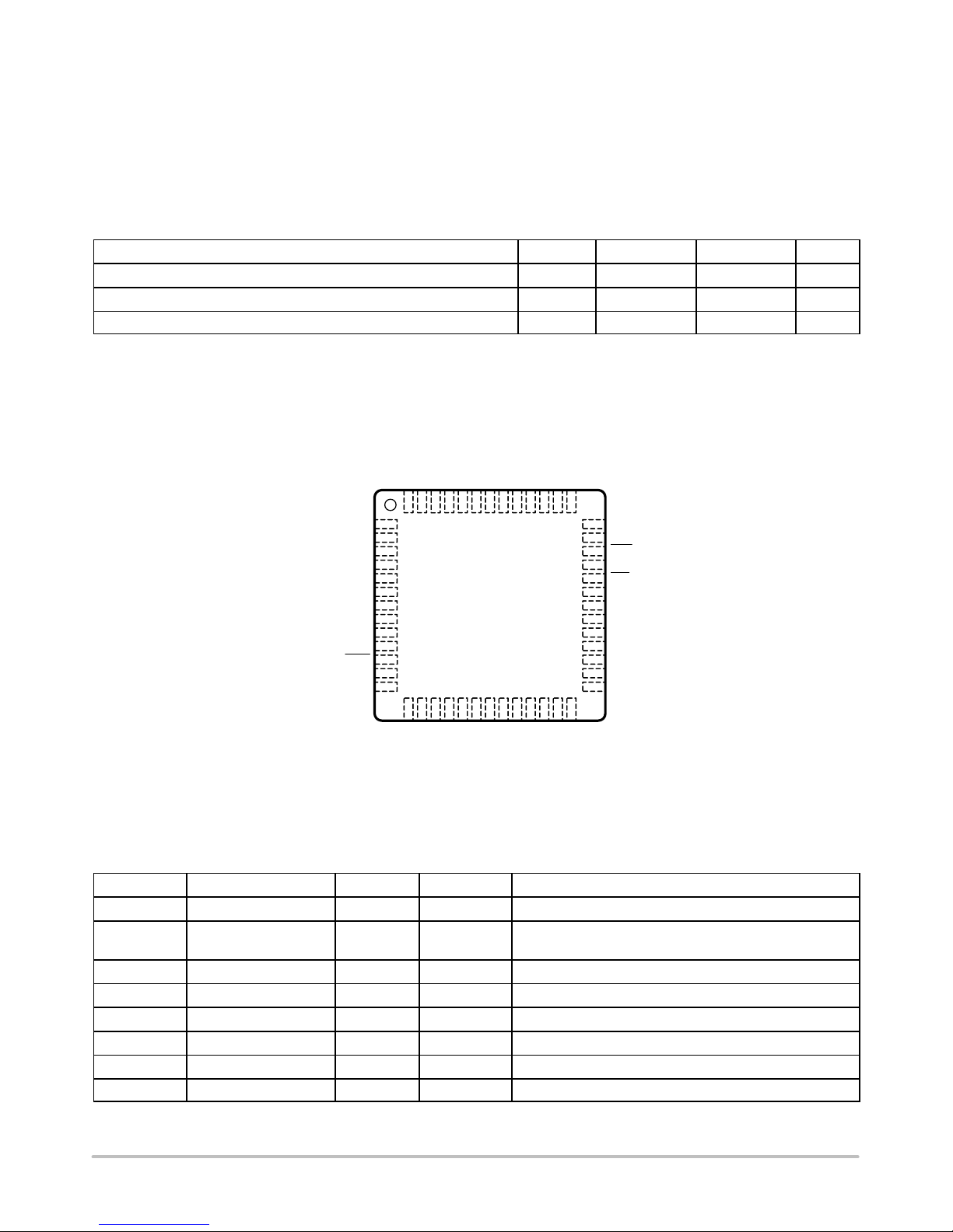
PIN DESCRIPTION
QFN Packaging
AMIS49597
1
2
3
4
5
6
7
8
9
10
11
12
13
26
25
24
23
22
21
20
19
18
17
16
15
14
39
38
37
36
35
34
33
32
31
30
29
28
27
40
41
42
43
44
45
46
47
48
49
50
51
52
NC
REF_O UT
NC
RX_IN
RX_OUT
VSSA
VDDA
NC
NC
ALC_IN
TX_OUT
NC
NC
IO8
IO9
TXD /PRES
XIN
XOUT
VDD 1V8
VSS
VDD
TXD
IO10
RXD
SCK
SDI
IO7
IO6
TMS
TCK
TDI
TDO
IO0/RX_DATA
IO5
IO4
IO3
NC
M50Hz _IN
SDO
CSB
T_REQ
SEN
BR1
BR0
CRC
IO11
TEST
NC
NC
TRST
RES
TX_EN
Figure 2. QFN Pin−out of NCN49597 (Top view)
Table 4. NCN49597QFN PIN FUNCTION DESCRIPTION
Pin No. Pin Name I/O Type Description
1 ZC_IN In A 50/60 Hz input for mains zero cross detection
3..5, 12..15,
23, 34
IO3 .. IO11 In/Out D, 5V Safe General Purpose I/O
6 RX_DATA Out D, 5V Safe Data reception indication (open drain output)
7 TDO Out D, 5V Safe Test data output
8 TDI In D, 5V Safe Test data input (internal pull down)
9 TCK In D, 5V Safe Test clock (internal pull down)
10 TMS In D, 5V Safe Test mode select (internal pull down)
11 TRSTB In D, 5V Safe Test reset bar (internal pull down, active low)
Page 5
NCN49597
http://onsemi.com
5
Table 4. NCN49597QFN PIN FUNCTION DESCRIPTION
Pin No. DescriptionTypeI/OPin Name
16 TXD/PRES Out D, 5V Safe Output of transmitted data (TXD) or PRE_SLOT signal
(PRES)
17 XIN In A Xtal input (can be driven by an internal clock)
18 XOUT Out A Xtal output (output floating when XIN driven by external
clock)
19 VDD1V8 P 1V8 regulator output. Foresee a decoupling capacitor
20 VSS P Digital ground
21 VDD P 3.3V digital supply
22 TXD Out D, 5V Safe SCI transmit output (open drain)
24 RXD In D, 5V Safe SCI receive input (Schmitt trigger output)
25 SCK Out D SPI interface external Flash
26 SDI In D SPI interface external Flash
27 SDO Out D SPI interface external Flash
28 CSB In D SPI interface external Flash
29 T_REQ In D, 5V Safe Transmit Request input
30 SEN In D Boot option
31 BR1 In D, 5V Safe SCI baud rate selection
32 BR0 In D, 5V Safe SCI baud rate selection
33 CRC Out D, 5V Safe Correct frame CRC indication (open drain output)
35 RESB In D, 5V Safe Master reset bar (Schmitt trigger input, active low)
36 TEST In D Hardware Test enable (internal pull down)
37 TX_ENB Out D, 5V Safe TX enable bar (open drain)
42 TX_OUT Out A Transmitter output
43 ALC_IN In A Automatic level control input
46 VDDA P 3.3V analog supply
47 VSSA P Analog ground
48 RX_OUT Out A Output of receiver low noise operational amplifier
49 RX_IN In A Positive input of receiver low noise operational amplifier
51 REF_OUT Out A Reference output for stabilization
2, 38..41, 44,
45,50, 52
NC Pins 2, 38..41, 44, 45, 50, 52 are not connected. These
pins need to be left open or connected to the GND plane.
P: Power pin 5V Safe: IO that support the presence of 5V on bus line
A: Analog pin Out: Output signal
D: Digital pin In: Input signal
Detailed Pin Description
VDDA
VDDA is the positive analog supply pin. Nominal voltage
is 3.3 V. A ceramic decoupling capacitor C
DA
= 100 nF must
be placed between this pin and the VSSA. Connection path
of this capacitance to the VSSA on the PCB should be kept
as short as possible in order to minimize the serial resistance.
REF_OUT
REF_OUT is the analog output pin which provides the
voltage reference used by the A/D converter. This pin must
be decoupled to the analog ground by a 1 mF ceramic
capacitance C
DREF
. The connection path of this capacitor to
Page 6
NCN49597
http://onsemi.com
6
the VSSA on the PCB should be kept as short as possible in
order to minimize the serial resistance.
VSSA
VSSA is the analog ground supply pin.
VDD
VDD is the 3.3 V digital supply pin. A ceramic decoupling
capacitor C
DD
= 100 nF must be placed between this pin and
the VSS. Connection path of this capacitance to the VSS on
the PCB should be kept as short as possible in order to
minimize the serial resistance.
VSS
VSS is the digital ground supply pin.
Figure 3: Recommended Layout of the Placement of
Decoupling Capacitors
VDD1V8
This is an additional power supply pin to decouple an
internal LDO regulator. The decoupling capacitor should be
placed as close as possible to this output pin as illustrated in
Figure 4.
RX_OUT
RX_OUT is the output analog pin of the receiver low
noise input op−amp. This op−amp is in a negative feedback
configuration.
RX_IN
RX_IN is the positive analog input pin of the receiver low
noise input op−amp. Together with RX_OUT and
REF_OUT, an active high pass filter is realized. This filter
removes the main frequency (50 or 60 Hz) from the received
signal. The filter characteristics are determined by external
capacitors and resistors. A typical application schematic can
be found in paragraph 50/60 Hz Suppression Filter.
ZC_IN
ZC_IN is the mains frequency analog input pin. The signal
is used to detect the zero cross of the 50 or 60 Hz sine wave.
This information is used, after filtering with the internal
PLL, to synchronize frames with the mains frequency. In
case of direct connection to the mains it is advised to use a
series resistor of 1 MW in combination with two external
clamp diodes in order to limit the current flowing through
the internal protection diodes.
RX_DATA
RX_DATA is a 5 V compliant open drain output. An
external pull−up resistor defines the logic high level as
illustrated in Figure 4. A typical value for the pull−up
resistance “R” is 10 kW. The signal on this output depends
on the status of the data reception. If NCN49597waits for
configuration RX_DATA outputs a pulse train with a 10 Hz
frequency. After Synchronization Confirm Time out
RX_DATA = 0. If NCN49597is searching for
synchronization RX_DATA = 1.
PC20090722. 2
V
SSD
+5V
Output
R
Figure 4. Representation of 5V Safe Output
TDO, TDI, TCK, TMS, and TRSTB
All these pins are part of the JTAG bus interface. The
JTAG interface is used during production test of the IC and
will not be described here. Input pins (TDI, TCK, TMS, and
TRSTB) contain internal pull−down resistance. TDO is an
output. When not used, the JTAG interface pins may be left
floating.
TXD/PRES
TXD/PRES is the output for either the transmitting data
(TX_DATA) or a synchronization signal with the time−slots
(PRE_SLOT). TXD/PRES. More information can be found
in paragraph Local Port.
XIN
XIN is the analog input pin of the oscillator. It is connected
to the interval oscillator inverter gain stage. The clock signal
can be created either internally with the external crystal and
two capacitors or by connecting an external clock signal to
XIN. For the internal generation case, the two external
capacitors and crystal are placed as shown in Figure 5. For
the external clock connection, the signal is connected to XIN
and XOUT is left unused.
Page 7
NCN49597
http://onsemi.com
7
XTAL_IN
PC20111118.1
XTAL_OUT
C
X
V
SSA
C
X
48 MHz
Figure 5. Placement of the Capacitors and Crystal
with Clock Signal Generated Internally
The crystal is a classical parallel resonance crystal of
48 MHz. The values of the capacitors C
X
are given by the
manufacturer of the crystal. A typical value is 36 pF. The
crystal has to fulfill impedance characteristics specified in
the NCN49597data sheet. As an oscillator is sensitive and
precise, it is advised to put the crystal as close as possible on
the board and to ground the case.
XOUT
XOUT is the analog output pin of the oscillator. When the
clock signal is provided from an external generator, this
output must be floating. When working with a crystal, this
pin cannot be used directly as clock output because no
additional loading is allowed on the pin (limited voltage
swing).
TXD
TXD is the digital output of the asynchronous serial
communication (SCI) unit. Only half−duplex transmission
is supported. It is used to realize the communication between
the NCN49597and the application microcontroller. The
TXD is an open drain IO (5 V safe). External pull−up
resistances (typically 10 kW) are necessary to generate the
5 V level. See Figure 4 for the circuit schematic.
RXD
This is the digital input of the asynchronous SCI unit.
Only half−duplex transmission is supported. This pin
supports a 5 V level. It is used to realize the communication
between the NCN49597and the application microcontroller.
RXD is a 5 V safe input.
T_REQ
T_REQ is the transmission request input of the Serial
Communication Interface. When pulled low its initiate a
local communication from the application micro controller
to NCN49597. T_REQ is a 5 V safe input. See also
paragraph Error! Reference source not found..
BR1, BR0
BR0 and BR1 are digital input pins. They are used to select
the baud rate (bits/second) of the Serial Communication
Interface unit. The rate is defined according to Error!
Reference source not found.. The values are taken into
account after a reset, hardware or software. Modification of
the baud rate during function is not possible. BR0 and BR1
are 5 V safe.
CRC
CRC is a 5 V compliant open drain output. An external
pull−up resistor defines the logic high level as illustrated in
Figure 4. A typical value for this pull−up resistance “R” is
10 kW. The signal on this output depends on the cyclic
redundancy code result of the received frame. If the cyclic
redundancy code is correct CRC = H during the pause
between two time slots.
RESB
RESB is a digital input pin. It is used to perform a
hardware reset of the NCN49597. This pin supports a 5 V
voltage level. The reset is active when the signal is low
(0 V).
TEST
TEST is a digital input pin with internal pull down resistor
used to enable the Hardware Test Mode of the chip. When
TEST is left open or forced to ground Normal Mode is
enabled. When TEST is forced to VDD the Hardware Test
Mode is enabled. This mode is used during production test
of the IC and will not be described here. TEST pin is not 5 V
safe.
TX_ENB
TX_ENB is a digital output pin. It is low when the
transmitter is activated. The signal is available to turn on the
line driver. TX_ENB is a 5 V safe with open drain output,
hence a pull−up resistance is necessary achieve the
requested voltage level associated with a logical one. See
also Figure 4 for reference.
TX_OUT
TX_OUT is the analog output pin of the transmitter. The
provided signal is the S−FSK modulated frames. A filtering
operation must be performed to reduce the second and third
order harmonic distortion. For this purpose an active filter
is suggested. See also paragraph Transmitter Output
TX_OUT.
ALC_IN
ALC_IN is the automatic level control analog input pin.
The signal is used to adjust the level of the transmitted
signal. The signal level adaptation is based on the AC
component. The DC level on the ALC_IN pin is fixed
internally to 1.65 V. Comparing the peak voltage of the AC
signal with two internal thresholds does the adaptation of the
gain. Low threshold is fixed to 0.4 V. A value under this
threshold will result in an increase of the gain. The high
threshold is fixed to 0.6 V. A value over this threshold will
result in a decrease of the gain. A serial capacitance is used
to block the DC components. The level adaptation is
performed during the transmission of the first two bits of a
new frame. Eight successive adaptations are performed. See
Page 8
NCN49597
http://onsemi.com
8
also paragraph Amplifier with Automatic Level Control
(ALC).
SCK, SDI, SDO, CSB
These signals from the SPI interface to an optional
external Flash. See Reference 1.
ELECTRICAL CHARACTERISTICS
DC and AC Characteristics
Oscillator: Pin XIN, XOUT
In production the actual oscillation of the oscillator and duty cycle will not be tested. The production test will be based on
the static parameters and the inversion from XIN to XOUT in order to guarantee the functionality of the oscillator.
Table 5. OSCILLATOR
Parameter Test Conditions Symbol Min Typ Max Unit
Crystal frequency (Note 1) f
CLK
−100 ppm 48 +100 ppm MHz
Duty cycle with quartz connected (Note 1) 40 60 %
Start−up time (Note 1) T
startup
50 ms
Load capacitance external crystal (Note 1) C
L
18 pF
Series resistance external crystal (Note 1) R
S
20 40 80
W
Maximum Capacitive load on
XOUT
XIN used as clock input CL
XOUT
50 pF
Low input threshold voltage XIN used as clock input VIL
XOUT
0.3 V
DD
V
High input threshold voltage XIN used as clock input VIH
XOUT
0.7 V
DD
V
Low output voltage XIN used as clock input,
XOUT = 2 mA
VOL
XOUT
0.3 V
High input voltage XIN used as clock input VOH
XOUT
V
DD
− 0.3 V
1. Guaranteed by design. Maximum allowed series loss resistance is 80 W
Page 9
NCN49597
http://onsemi.com
9
Zero Cross Detector and 50/60 Hz PLL: Pin ZC_IN
Table 6. ZERO CROSS DETECTOR AND 50/60 HZ PLL
Parameter Test Conditions Symbol Min Typ Max Unit
Maximum peak input current Imp
ZC_IN
−20 20 mA
Maximum average input current During 1 ms Imavg
ZC_IN
−2 2 mA
Mains voltage (ms) range With protection resistor at
ZC_IN
V
MAINS
90 550 V
Rising threshold level (Note 2) VIR
ZC_IN
1.9 V
Falling threshold level (Note 2) VIF
ZC_IN
0.9 V
Hysteresis (Note 2) VHY
ZC_IN
0.4 V
Lock range for 50 Hz (Note 3) MAINS_FREQ = 0 (50 Hz) Flock
50Hz
45 55 Hz
Lock range for 60 Hz (Note 3) MAINS_FREQ = 0 (60 Hz) Flock
60Hz
54 66 Hz
Lock time (Note 3) MAINS_FREQ = 0 (50 Hz) Tlock
50Hz
15 s
Lock time (Note 3) MAINS_FREQ = 0 (60 Hz) Tlock
60Hz
20 s
Frequency variation without going
out of lock (Note 3)
MAINS_FREQ = 0 (50 Hz) DF
60Hz
0.1 Hz/s
Frequency variation without going
out of lock (Note 3)
MAINS_FREQ = 0 (60 Hz) DF
50Hz
0.1 Hz/s
Jitter of CHIP_CLK (Note 3) Jitter
CHIP_CLK
−25 25
ms
2. Measured relative to VSS
3. These parameters will not be measured in production since the performance is totally dependent of a digital circuit which will be guaranteed
by the digital test patterns.
Page 10

NCN49597
http://onsemi.com
10
Transmitter External Parameters: Pin TX_OUT, ALC_IN, TX_ENB
To guarantee the transmitter external specifications the TX_CLK frequency must be 12 MHz ± 100 ppm.
Table 7. TRANSMITTER EXTERNAL PARAMETERS
Parameter Test Conditions Symbol Min Ty p Max Unit
Maximum peak output level f
TX_OUT
= 23 – 75 kHz
f
TX_OUT
= 95 kHz
Level control at max. output
V
TX_OUT
0.85
0.76
1.15
1.22
Vp
Second order harmonic distortion f
TX_OUT
= 95 kHz
Level control at max. output
HD2 −54 dB
Third order harmonic distortion f
TX_OUT
= 95 kHz
Level control at max. output
HD3 −53 dB
Frequency accuracy of the generated sine wave
(Notes 4 and 6) Df
TX_OUT
30 Hz
Capacitive output load at pin
TX_OUT
(Note 4) CL
TX_OUT
20 pF
Resistive output load at pin
TX_OUT
RL
TX_OUT
5
kW
Turn off delay of TX_ENB output (Note 5) Td
TX_ENB
0.25 0.5 ms
Automatic level control attenuation
step
ALC
step
2.9 3.1 dB
Maximum attenuation ALC
range
20.3 21.7 dB
Low threshold level on ALC_IN VTL
ALC_IN
−0.46 −0.36 V
High threshold level on ALC_IN VTH
ALC_IN
−0.68 −0.54 V
Input impedance of ALC_IN pin R
ALC_IN
111 189
kW
Power supply rejection ration of the
transmitter section
PSRR
TX_OUT
10
(Note 7)
35
(Note 8)
dB
4. This parameter will not be tested in production.
5. This delay corresponds to the internal transmit path delay and will be defined during design.
6. Taking into account the resolution of the DDS and an accuracy of 100ppm of the crystal.
7. A sinusoidal signal of 10 kHz and 100 mVpp is injected between VDDA and VSSA. The digital AD converter generates an idle pattern. The
signal level at TX_OUT is measured to determine the parameter.
8. A sinusoidal signal of 50 Hz and 100 mVpp is injected between VDDA and VSSA. The digital AD converter generates an idle pattern. The
signal level at TX_OUT is measured to determine the parameter.
The LPF filter + amplifier must have a frequency characteristic between the limits listed below. The absolute output level
depends on the operating condition. In production the measurement will be done for relative output levels where the 0 dB
reference value is measured at 50 kHz with a signal amplitude of 100 mV.
Table 8. TRANSMITTER FREQUENCY CHARACTERISTICS
Frequency (kHz)
Attenuation
Unit
Min Max
10 −0.5 0.5 dB
95 −1.3 0.5 dB
130 −4.5 −2.0 dB
165 −3.0 dB
330 −18.0 dB
660 −36.0 dB
1000 −50 dB
2000 −50 dB
Page 11

NCN49597
http://onsemi.com
11
Receiver External Parameters: Pin RX_IN, RX_OUT, REF_OUT
Table 9. RECEIVER EXTERNAL PARAMETERS
Parameter Test Conditions Symbol Min Ty p Max Unit
Input offset voltage 42 dB AGC gain = 42 dB V
OFFS_RX_IN
5 mV
Input offset voltage 0 dB AGC gain = 0 dB V
OFFS_RX_IN
50 mV
Max. peak input voltage (corresponding to 62.5% of the SD full
scale)
AGC gain = 0 dB (Note 9) V
MAX_RX_IN
0.85 1.15 Vp
Input referred noise of the analog
receiver path
AGC gain = 42 dB
(Notes 9 and 10)
NF
RX_IN
150 nV/ǠHz
Input leakage current of receiver
input
I
LE_RX_IN
−1 1
mA
Max. current delivered by
REF_OUT
I
Max_REF_OUT
−300 300 mA
Power supply rejection ratio of the
receiver input section
AGC gain = 42 dB (Note 11)
PSRR
LPF_OUT
10 dB
AGC gain = 42 dB (Note 12) 35
AGC gain step AGC
step
5.7 6.3 dB
AGC range AGC
range
39.9 44.1 dB
Analog ground reference output
voltage
V
REF_OUT
1.52 1.78 V
Signal to noise ratio at 62.5 % of
the SD full scale
(Notes 9 and 13) SN
AD_OUT
54 dB
Clipping level at the output of the
gain stage (RX_OUT)
V
CLIP_AGC_IN
1.15 1.65 Vp
9. Input at RX_IN, no other external components.
10.Characterization data only. Not tested in production.
11.A sinusoidal signal of 10 kHz and 100 mVpp is injected between VDDA and VSSA. The signal level at the differential LPF_OUT and
REF_OUT output is measured to determine the parameter.
12.A sinusoidal signal of 50 Hz and 100 mVpp is injected between VDDA and VSSA. The signal level at the differential LPF_OUT output is
measured to determine the parameter.
13.These parameters will be tested in production with an input signal of 95 kHz and 1 Vp by reading out the digital samples at the point AD_OUT
with the default settings of T_RX_MOD[7], SDMOD_TYP, DEC_TYP, and COR_F_ENA. The AGC gain is switched to 0 dB.
The receive LPF filter + AGC + low noise amplifier must have a frequency characteristic between the limits listed below.
The absolute output level depends on the operating condition.
Table 10. RECEIVER FREQUENCY CHARACTERISTICS
Frequency (kHz)
Attenuation
Unit
Min Max
10 −0.5 0.5 dB
95 −1.3 0.5 dB
130 −4.5 −2.0 dB
165 −3.0 dB
330 −18.0 dB
660 −36.0 dB
1000 −50 dB
2000 −55 dB
Page 12

NCN49597
http://onsemi.com
12
Power−on−Reset (POR)
Table 11. POWER−ON−RESET
Parameter Test Conditions Symbol Min Ty p Max Unit
POR threshold V
POR
1.7 2.7 V
Power supply rise time 0 to 3V T
RPOR
1 ms
Digital Outputs: TDO, CLK_OUT
Table 12. DIGITAL OUTPUTS: TDO, CLK_OUT
Parameter Test Conditions Symbol Min Ty p Max Unit
Low output voltage I
XOUT
= 4 mA V
OL
0.4 V
High output voltage I
XOUT
= −4 mA V
OH
0.85 V
DD
V
Digital Outputs with Open Drain: TX_ENB, TXD
Table 13. DIGITAL OUTPUTS WITH OPEN DRAIN: TX_ENB, TXD, RX_DATA, CRC, T_REQ
Parameter Test Conditions Symbol Min Ty p Max Unit
Low output voltage I
XOUT
= 4 mA V
OL
0.4 V
Digital Inputs: BR0, BR1
Table 14. DIGITAL INPUTS: BR0, BR1
Parameter Test Conditions Symbol Min Ty p Max Unit
Low input level V
IL
0.2 V
DD
V
High input level 0 to 3 V V
IH
0.8 V
DD
V
Input leakage current I
LEAK
−10 10
mA
Digital Inputs with Pull Down: TDI, TMS, TCK, TRSTB, TEST
Table 15. DIGITAL INPUTS WITH PULL DOWN: TDI, TMS, TCK, TRSTB, TEST
Parameter Test Conditions Symbol Min Ty p Max Unit
Low input level V
IL
0.2 V
DD
V
High input level V
IH
0.8 V
DD
V
Pull down resistor (Note 14) R
PU
7 50
kW
14.Measured around a bias point of VDD/2.
Digital Schmitt Trigger Inputs: RXD, RESB
Table 16. DIGITAL SCHMITT TRIGGER INPUTS: RXD, RESB
Parameter Test Conditions Symbol Min Ty p Max Unit
Rising threshold level V
T+
0.80 V
DD
V
Falling threshold level V
T−
0.2 V
DD
V
Input leakage current I
LEAK
−10 10
mA
Page 13

NCN49597
http://onsemi.com
13
Current Consumption
Table 17. CURRENT CONSUMPTION
Parameter Test Conditions Symbol Min Ty p Max Unit
Current consumption in receive
mode
Current through V
DD
and V
DDA
(Note 15)
I
RX
60 80 mA
Current consumption in transmit
mode
Current through V
DD
and V
DDA
(Note 15)
I
TX
60 80 mA
Current consumption when RESB
= 0
Current through V
DD
and V
DDA
(Note 15)
I
RESET
4 mA
15.f
CLK
= 48 MHz.
INTRODUCTION
General Description
The NCN49597 is a single chip half duplex S−FSK
modem dedicated to power line carrier (PLC) data
transmission on low− or medium−voltage power lines. The
device offers complete handling of the protocol layers from
the physical up to the MAC. NCN49597 complies with the
CENELEC EMC standard EN 50065−1 and the
IEC 61334−5−1 standards. It operates from a single 3.3 V
power supply and is interfaced to the power line by an
external power driver and transformer. An internal PLL is
locked to the mains frequency and is used to synchronize the
data transmission at data rates of 300, 600, 1200, 2400 and
4800 baud for a 50 Hz mains frequency, or 360, 720, 1440,
2880 and 5760 baud for a 60 Hz mains frequency. In both
cases this corresponds to 3, 6, 12 or 24 data bits per half cycle
of the mains period.
S−FSK is a modulation and demodulation technique that
combines some of the advantages of a classical spread
spectrum system (e.g. immunity against narrow band
interferers) with the advantages of the classical FSK system
(low complexity). The transmitter assigns the space
frequency f
S to “data 0” and the mark frequency fM to
“data 1”. The difference between S−FSK and the classical
FSK lies in the fact that f
S and fM are now placed far from
each other, making their transmission quality independent
from each other (the strengths of the small interferences and
the signal attenuation are both independent at the two
frequencies). The frequency pairs supported by the
NCN49597 are in the range of 9 − 150 kHz with a typical
separation of 10 kHz.
The conditioning and conversion of the signal is
performed at the analog front−end of the circuit. The further
processing of the signal and the handling of the protocol is
digital. At the back−end side, the interface to the application
is done through a serial interface. The digital processing of
the signal is partitioned between hardwired blocks and a
microprocessor block. The microprocessor is controlled by
firmware. Where timing is most critical, the functions are
implemented with dedicated hardware. For the functions
where the timing is less critical, typically the higher level
functions, the circuit makes use of the ARM microprocessor
core.
The processor runs DSP algorithms and, at the same time,
handles the communication protocol. The communication
protocol, in this application, contains the MAC = Medium
Access Control Layer. The program running on the
microprocessor is stored into ROM. The working data
necessary for the processing is stored in an internal RAM. At
the back−end side the link to the application hardware is
provided by a Serial Communication Interface (SCI). The
SCI is an easy to use serial interface, which allows
communication between an external processor used for the
application software and the NCN49597 modem. The SCI
works on two wires: TXD and RXD. Baud rate is
programmed by setting 2 bits (BR0, BR1).
Because the low protocol layers are handled in the circuit,
the NCN49597 provides an innovative architectural split.
Thanks to this, the user has the benefit of a higher level
interface of the link to the PLC medium. Compared to an
interface at the physical level, the NCN49597 allows faster
development of applications. The user just needs to send the
raw data to the NCN49597 and no longer has to take care of
the protocol detail of the transmission over the specific
medium. This last part represents usually 50% of the
software development costs.
Page 14

NCN49597
http://onsemi.com
14
Minor User TypeMajor User Type
PC 201111 12 .2
SPY
Application
NCN49597in
MONITOR mode
TEST
Application
NCN49597in
TEST mode
CLIENT
Application
NCN49597in
MASTER mode
SERVER
Application
NCN49597in
SLAVE mode
SERVER
Application
NCN49597in
SLAVE mode
Figure 6. Application Examples
NCN49597 is intended to connect equipment using
Distribution Line Carrier (DLC) communication. It serves
two major and two minor types of applications:
• Major types:
♦ Master or Client:
A Master is a client to the data served by one or
many slaves on the power line. It collects data from
and controls the slave devices. A typical application
is a concentrator system
♦ Slave or Server:
A Slave is a server of the data to the Master. A
typical application is an electricity meter equipped
with a PLC modem.
• Minor type:
♦ Spy or Monitor:
Spy or Monitor mode is used to only listen to the
data that comes across the power line. Only the
physical layer frame correctness is checked. When
the frame is correct, it is passed to the external
processor.
♦ Test Mode:
The Software Test Mode is used to test the
compliance of a PLC modem conforms to
CENELEC. EN 50065−1 by a continuous broadcast
of f
S
or fM.
Page 15

NCN49597
http://onsemi.com
15
Functional Description
The block diagram below represents the main functional units of the NCN49597:
Communication Controller
ARM
Risc
Core
Serial
Comm.
Interface
Local Port
Test
Control
POR
Watchdog
Timer 1 & 2
SPI
Interrupt
Control
Data
RAM
Program
ROM
AAF AGC A/D
REF
S−FSK
Demodulator
Receiver (S−FSK Demodulator)
Clock and Control
Zero
crossing
PLL OSC
Clock Generator
& Timer
Transmit Data
& Sine Synthesizer
D/A
LP
Filter
Transmitter (S−FSK Modulator)
RX_DATA
RESB
JTAG I/F
TEST
TX_ENB
TX_OUT
ALC_IN
RX_OUT
RX_IN
REF_OUT
M50Hz_IN
XIN XOUTVDDA VSSA VDDD VSSD
NCN49597
PC20111019.2
TO Power Amplifier
FROM Line Coupler
TO Application
Micro Controller
TxD
RxD
T_REQ
BR0
BR1
CRC
TX_DATA / PRE _SLOT
5
VDD1V8
IO[9:3]
5
SPI I/F
5
Figure 7. S−FSK Modem NCN49597 Block Diagram
Transmitter
The NCN49597 Transmitter function block prepares the
communication signal which will be sent on the
transmission channel during the transmitting phase. This
block is connected to a power amplifier which injects the
output signal on the mains through a line−coupler.
Receiver
The analog signal coming from the line−coupler is low
pass filtered in order to avoid aliasing during the conversion.
Then the level of the signal is automatically adapted by an
automatic gain control (AGC) block. This operation
maximizes the dynamic range of the incoming signal. The
signal is then converted to its digital representation using
sigma delta modulation. From then on, the processing of the
data is done in a digital way. By using dedicated hardware,
a direct quadrature demodulation is performed. The signal
demodulated in the base band is then low pass filtered to
reduce the noise and reject the image spectrum.
Clock and Control
According to the IEC 61334−5−1 standard, the frame data
is transmitted at the zero cross of the mains voltage. In order
to recover the information at the zero cross, a zero cross
detection of the mains is performed. A phase−locked loop
(PLL) structure is used in order to allow a more reliable
reconstruction of the synchronization. This PLL permits as
well a safer implementation of the ”repetition with credit”
function (also known as chorus transmission). The clock
generator makes use of a precise quartz oscillator master.
The clock signals are then obtained by the use of a
programmed division scheme. The support circuits are also
contained in this block. The support circuits include the
necessary blocks to supply the references voltages for the
AD and DA converters, the biasing currents and power
supply sense cells to generate the right power off and startup
conditions.
Page 16

NCN49597
http://onsemi.com
16
48 bit @ 2400 baud
20 ms
t
PC20100609.1
Figure 8. Data Stream is in Sync with Zero Cross of the Mains (example for 50 Hz)
Communication Controller
The Communication Controller block includes the
micro−processor, its peripherals: RAM, ROM, UART,
TIMER, and the Power on reset. The processor uses the
ARM Reduced Instruction Set Computer (RISC)
architecture optimized for IO handling. For most of the
instructions, the machine is able to perform one instruction
per clock cycle. The microcontroller contains the necessary
hardware to implement interrupt mechanisms, timers and is
able to perform byte multiplication over one instruction
cycle. The microcontroller is programmed to handle the
physical layer (chip synchronization), and the MAC layer
conform to IEC 61334−5−1. The program is stored in a
masked ROM. The RAM contains the necessary space to
store the working data. The back−end interface is done
through the Serial Communication Interface block. This
back−end is used for data transmission with the application
micro controller (containing the application layer for
concentrator, power meter, or other functions) and for the
definition of the modem configuration.
Local Port
The controller uses 3 output ports to inform about the
actual status of the PLC communication. RX_DATA
indicates if Receiving is in progress, or if NCN49597 is
waiting for synchronization, or of it configures. CRC
indicates if the received frames are valid (CRC = OK).
TXD/PRES is the output for either the transmitting data
(TX_DATA) or a synchronization signal with the time−slots
(PRE_SLOT).
Serial Communication Interface
The local communication is a half duplex asynchronous
serial link using a receiving input (RxD) and a transmitting
output (TxD). The input port T_REQ is used to manage the
local communication with the application micro controller
and the baud rate can be selected depending on the status of
two inputs BR0, BR1. These two inputs are taken in account
after an NCN49597 reset. Thus when the application micro
controller wants to change the baud rate, it has to set the two
inputs and then provoke a reset.
DETAILED HARDWARE DESCRIPTION
Clock and Control
According to the IEC 61334−5−1 standard, the frame data
is transmitted at the zero cross of the mains voltage. In order
to recover the information at the zero cross, a zero cross
detection of the mains is performed. A phase−locked loop
(PLL) structure is used in order to allow a more reliable
reconstruction of the synchronization. The output of this
block is the clock signal CHIP_CLK, 8 times over sampled
with the bit rate. The oscillator makes use of precise 48 MHz
quartz. This clock signal together with CHIP_CLK is fed
into the Clock Generator and time block. Here several
internal clock signals and timings are obtained by the use of
a programmed division scheme.
Page 17

NCN49597
http://onsemi.com
17
Clock and Control
Zero
crossing
PLL OSC
Clock Generator
& Timer
ZC_IN
XIN XOUT
PC20090619.4
BIT_CLK
BYTE_CLK
FRAME_CLK
PRE_BYTE_CLK
PRE_FRAME_CLK
PRE_SLOT
CHIP_CLK
Figure 9. Clock and Control Block
Zero Cross Detector
ZC_IN is the mains frequency analog input pin. The signal
is used to detect the zero cross of the 50 or 60 Hz sine wave.
This information is used, after filtering with the internal
PLL, to synchronize frames with the mains frequency. In
case of direct connection to the mains it is advised to use a
series resistor of 1 MW in combination with two external
Schottky clamp diodes in order to limit the current flowing
through the internal protection diodes.
FROM
MAINS
Clock & Control
ZC_IN
ZeroCross
PLL
CHIP_CLK
Debounce
Filter
3V3_A
1MW
PC20100608.1
100 pF
BAS70−04
Figure 10. Zero Cross Detector with Falling Edge De−bounce Filter
The zero cross detector output is logic zero when the input
is lower than the falling threshold level and a logic one when
the input is higher than the rising threshold level. The falling
edges of the output of the zero cross detector are de−bounced
by a period between 0.5 ms and 1 ms. The Rising edges are
not de−bounced.
Page 18

NCN49597
http://onsemi.com
18
t
10 ms
V
MAINS
ZeroCross
t
ZCD
VIR
ZC_ IN
PC20090620 .1
VIF
ZC_ IN
t
DEBOUNCE
= 0,5 .. 1 ms
Figure 11. Zero Cross Detector Signals and Timing (example for 50 Hz)
50/60 Hz PLL
The output of the zero cross detector is used as an input for
a PLL. The PLL generates the clock CHIP_CLK which is 8
times the bit rate and which is in phase with the rising edge
crossings. The PLL locks on the zero cross from negative to
positive phase. The bit rate is always an even multiple of the
mains frequency, so following combinations are possible:
Table 18. CHIP_CLK IN FUNCTION OF SELECTED BAUD RATE AND MAINS FREQUENCY
BAUD[1:0] MAINS_FREQ Baudrate CHIP_CLK
00
50 Hz
300 2400 Hz
01 600 4800 Hz
10 1200 9600 Hz
11 2400 19200 Hz
00
60 Hz
360 2880 Hz
01 720 5760 Hz
10 1440 11520 Hz
11 2880 23040 Hz
In case no zero crossings are detected the PLL freezes its internal timers in order to maintain the CHIP_CLK timing.
Page 19

NCN49597
http://onsemi.com
19
6 bit @ 300 baud
t
10 ms
V
MAINS
ZeroCross
t
ZCD
VIR
ZC _IN
CHIP _CLK
PC 20090 619 .3
PLL in lock
Start of Physical PreFrame (*)
*The start of the Physical Subframe is shifted back with R_ZC_ADJUST[7:0] x 26 mS = t
ZCD
to compensate for the zero cross delay.
Figure 12. Zero Cross Adjustment to Compensate for Zero Cross Delay (example for 50 Hz)
The phase difference between the zero cross of the mains
and CHIP_CLK can be tuned. This opens the possibility to
compensate for external delay t
ZCD
(e.g. opto coupler) and
for the 1.9 V positive threshold VIR
ZC_IN
of the zero cross
detector. This is done by pre−loading the PLL counter with
a number value stored in register R_ZC_ADJUST[7:0]. The
adjustment period or granularity is 26 ms. The maximum
adjustment is 255 x 26 ms = 6.6 ms which corresponds with
1/3rd of the 50 Hz mains sine period.
Table 19. ZERO CROSS DELAY COMPENSATION
R_ZC_ADJUST[7:0] Compensation
0000 0000
0 ms
0000 0001
26 ms
0000 0010
52 ms
0000 0011
78 ms
… …
1111 11 0 1
6589 ms
1111 111 0
6615 ms
1111 1111
6641 ms
Oscillator
The oscillator works with a standard parallel resonance
crystal of 48 MHz. XIN is the input to the oscillator inverter
gain stage and XOUT is the output.
Page 20

NCN49597
http://onsemi.com
20
XTAL_IN
PC20111118.1
XTAL_OUT
C
X
V
SSA
C
X
48 MHz
Figure 13. Placement of the Capacitors and Crystal
with Clock Signal Generated Internally
For correct functionality the external circuit illustrated in
Figure 13 must be connected to the oscillator pins. For a
crystal requiring a parallel capacitance of 18 pF C
X
must be
around 36 pF. (Values of capacitors are indicative only and
are given by the crystal manufacturer). To guarantee startup
the series loss resistance of the crystal must be smaller than
60 W.
The oscillator output f
CLK
= 48 MHz is the base frequency
for the complete IC. The clock frequency for the ARM f
ARM
= f
CLK.
The clock for the transmitter, f
TX_CLK
is equal to
f
CLK
/ 4 or 12 MHz. All the transmitter internal clock signals
will be derived from f
TX_CLK
. The clock for the receiver,
f
RX_CLK
is equal to f
CLK
/ 8 or 6 MHz. All the receiver
internal clock signals will be derived from f
RX_CLK.
Clock Generator and Timer
The CHIP_CLK and f
CLK
are used to generate a number
of timing signals used for the synchronization and interrupt
generation. The timing generation has a fixed repetition rate
which corresponds to the length of a physical subframe. (see
paragraph Error! Reference source not found.)
The timing generator is the same for transmit and receive
mode. When NCN49597 switches from receive to transmit
and back from transmit to receive, the R_CHIP_CNT
counter value is maintained. As a result all timing signals for
receive and transmit have the same relative timing. The
following timing signals are defined as:
BIT_CLK
63 64 652871 2872 102879 2 3 4 5 6 7 8 9
CHIP_CLK
BYTE_CLK
FRAME_CLK
PRE_FRAME_CLK
PRE_BYTE_CLK
R_CHIP_CNT
PRE_SLOT
PC20090619.1
Start of the physical subframe
Figure 14. Timing Signals
CHIP_CLK: is the output of the PLL and 8 times the bit rate
on the physical interface. See also paragraph 50/60 Hz PLL.
BIT_CLK: is active at counter values 0, 8, 16, .. 2872 and
inactive at all other counter values. This signal is used to
indicate the transmission of a new bit.
BYTE_CLK: is active at counter values 0, 64, 128, .. 2816
and inactive at all other counter values. This signal is used
to indicate the transmission of a new byte.
Page 21

NCN49597
http://onsemi.com
21
FRAME_CLK: is active at counter values 0 and inactive at
all other counter values. This signal is used to indicate the
transmission or reception of a new frame.
PRE_BYTE_CLK is a signal which is 8 CHIP_CLK
sooner than BYTE_CLK. This signal is used as an interrupt
for the internal microcontroller and indicates that a new byte
for transmission must be generated.
PRE_FRAME_CLK is a signal which is 8 CHIP_CLK
sooner than FRAME_CLK. This signal is used as an
interrupt for the internal microcontroller and indicates that
a new frame will start at the next FRAME_CLK.
PRE_SLOT is logic 1 between the rising edge of
PRE_FRAME_CLK and the rising edge of FRAME_CLK.
This signal can be provided at the digital output pin
TXD/PRES when R_CONF[7] = 0 (See paragraph Local
Port and Error! Reference source not found., field
R_CONF_TXD_PRES_SEL) and can be used by the external
host controller to synchronize its software with the
FRAME_CLK of NCN49597.
Transmitter Path Description (S−FSK Modulator)
For the generation of the space and mark frequencies, the
direct digital synthesis (DDS) of the sine wave signals is
performed under the control of the microprocessor. After a
signal conditioning step, a digital to analog conversion is
performed. As for the receive path, a sigma delta modulation
technique is used. In the analog domain, the signal is low
pass filtered, in order to remove the high frequency
quantization noise, and passed to the automatic level
controller (ALC) block, where the level of the transmitted
signal can be adjusted. The determination of the signal level
is done through the sense circuitry.
Transmitter(S−FSK Modulator)
PC20091019.1
ARM
Interface
&
Control
TX_OUT
Transmit Data
& Sine Synthesizer
D/A
LP
Filter
ALC
control
ALC_IN
TO RECEIVER
f
MIfMQfSIfSQ
TX_EN
Figure 15. Transmitter Block Diagram
ARM Interface and Control
The interface with the ARM consists in a 8−bit data
registers R_TX_DATA, 2 control registers R_TX_CTRL
and R_ALC_CTRL, a flag TX_RXB defining transmit and
receive and 2 16−bit wide frequency step registers R_FM
and R_FS defining f
M
(mark frequency = data 1) and f
S
(space frequency = data 0). All these registers are memory
mapped. Some of them are for internal use only and cannot
be accessed by the user.
Processing of the physical frame (preamble, MAC
address, CRC) is done by the ARM.
Sine Wave Generator
A sine wave is generated with a direct digital synthesizer
DDS. The synthesizer generates in transmission mode a sine
wave either for the space frequency (f
S
, data 0) or for the
mark frequency (f
M
, data1). In reception the synthesizer
generates the sine and cosine waves for the mixing process,
f
SI
, fSQ, fMI, fMQ (space and mark signals in phase and
quadrature). The space and mark frequencies are defined in
an individual step 16 bit wide register.
Table 20. FS AND FM STEP REGISTERS
ARM Register Hard Reset Soft Reset Description
R_FS[15:0] 0000h 0000h Step register for the space frequency f
S
R_FM[15:0] 0000h 0000h Step register for the mark frequency f
M
Page 22

NCN49597
http://onsemi.com
22
The space and mark frequency can be calculated as:
• f
S
= R_FS[15:0]_dec x f
DDS
/2
18
• f
M
= R_FM[15:0]_dec x f
DDS
/2
18
Or the content of both R_FS[15:0] and R_FM[15:0] are
defined as:
• R_FS[15:0]_dec = Round(2
18
x fS/f
DDS
)
• R_FM[15:0]_dec = Round(2
18
x fM/f
DDS
)
♦ Where f
DDS
= 3 MHz is the direct digital
synthesizer clock frequency.
After a hard or soft reset or at the start of the transmission
(when TX_RXB goes from 0 to 1) the phase accumulator
must start at it’s 0 phase position, corresponding with a 0 V
output level. When switching between f
M
and fS the phase
accumulator must give a continuous phase and not restart
from phase 0
When NCN49597 goes into receive mode (when
TX_RXB goes from 1 to 0) the sine wave generator must
make sure to complete the active sine period.
The control logic for the transmitter generates a signal
TX_ENB to enable the external power amplifier. TX_ENB
is 1 when the NCN49597 is in receive mode. TX_ENB is 0
when NCN49597is in transmit mode. When going from
transmit to receive mode (TX_RXB goes from 1 to 0) the
TX_ENB signal is kept active for a short period of t
dTX_ENB
.
The control logic for the transmitter generates a signal
TX_DATA which corresponds to the transmitted S−FSK
signal. When transmitting f
M
TX_DATA is logic 1. When
transmitting f
S
TX_DATA is logic 0. When the transmitter
is not enabled (TX_RXB = 0) TX_DATA goes to logic 1 at
the next BIT_CLK.
PC20090610.1
TX_DATA
TX_RXB
t
dTX_ENB
BIT_CLK
TX_ENB
TX_OUT
Figure 16. TX_ENB Timing
DA Converter
A digital to analog SD converter converts the sine wave
digital word to a pulse density modulated (PDM) signal. The
PDM signal is converted to an analog signal with a first order
switched capacitor filter.
Low Pass Filter
A 3rd order continuous time low pass filter in the transmit
path filters the quantization noise and noise generated by the
ΣΔ DA converter. The typical corner frequency f
−3dB
= 138
kHz and is internally trimmed to compensate for process
variation. This filter can be tuned to f
−3dB
= 1508 kHz as
described in reference [1].
Amplifier with Automatic Level Control (ALC)
The pin ALC_IN is used for level control of the
transmitter output level. First peak detection is done. The
peak value is compared to two thresholds levels:
VTL
ALC_IN
and VTH
ALC_IN
. The result of the peak
detection is used to control the setting of the level of
TX_OUT. The level of TX_OUT can be attenuated in 8 steps
of 3 dB typical.
After hard or soft reset the level is set at minimum level
(maximum attenuation) When going to reception mode
(when TX_RXB goes from 1 to 0) the level is kept in
memory so that the next transmit frame starts with the old
level. The evaluation of the level is done during 1
CHIP_CLK period.
Depending on the value of peak level on ALC_IN the
attenuation is updated:
• Vp
ALC_IN
< VTL
ALC
: increase the level with one 6 dB
step
• VTL
ALC
≤ Vp
ALC_IN
≤ VTH
ALC
: don’t change the
level
• Vp
ALC_IN
> VTH
ALC
: decrease the level with one 6 dB
step
Page 23

NCN49597
http://onsemi.com
23
The gain changes in the next CHIP_CLK period.
An evaluation phase and a level adjustment take 2
CHIP_CLK periods. ALC operation is enabled only during
the first 16 CHIP_CLK cycles after a hard or soft reset or
after going into transmit mode.
The automatic level control can be disabled by setting
register R_ALC_CTRL[3] = 1. In this case the transmitter
output level is fixed to the programmed level in the register
R_ALC_CTRL[2:0]. See Reference 1.
Table 21. FIXED TRANSMITTER OUTPUT ATTENUATION
ALC_CTRL[2:0] Attenuation
000 0 dB
001 −3 dB
010 −6 dB
011 −9 dB
100 −12 dB
101 −15 dB
110 −18 dB
111 −21 dB
Remark:
Transmitter Output TX_OUT
The transmitter output is DC coupled to the TX_OUT pin.
Because the complete analog part of NCN49597 is
referenced to the analogue ground REF_OUT, a decoupling
capacitor C
1
is needed when connecting NCN49597 to
external circuitry working with another ground. To suppress
the second and third order harmonic of the generated S−FSK
signal it is recommended to use a 2
nd
or 4th order low pass
filter. In Figure 17 a MFB topology of a 2
nd
order filter is
illustrated.
ALC
control
ALC _IN
Transmitter (S−FSK Modulator )
PC 20091216.1
ARM
Interface
&
Control
TX_OUT
LP
Filter
TX_EN
TO TX POWER
OUTPUT STAGE
FROM LINE
DRIVER
C
1
R
1
V
SSA
C
2
R
2
R
3
C
3
C
4
R
4
Figure 17. TX_OUT Filter
Receiver Path Description
Receiver Block Diagram
The receiver takes in the analog signal from the line
coupler, conditions it and demodulates it in a data−stream to
the communication controller. The operation mode and the
baud rate are made according to the setting in R_CONF,
R_FS and R_FM. The receive signal is applied first to a high
pass filter. Therefore NCN49597 has a low noise operational
amplifier at the input stage which can be used to make a high
pass active filter to attenuate the mains frequency. This high
pass filter output is followed by a gain stage which is used
in an automatic gain control loop. This block also performs
a single ended input to differential output conversion. This
gain stage is followed by a continuous time low pass filter
to limit the bandwidth. A 4
th
order sigma delta converter
converts the analog signal to digital samples. A quadrature
demodulation for f
S
and fM is than performed by an internal
DSP, as well the handling of the bits and the frames.
Page 24

NCN49597
http://onsemi.com
24
RX_OUT
RX_IN
REF_OUT
PC20090610.2
LOW NOISE
OPAMP
REF
1,65 V
TO
DIGITAL
Receiver (Analog Path)
Gain LPF
4th
order
SD AD
FROM
DIGITAL
Figure 18. Analog Path of the Receiver
PC20110610.3
Abs
value
accu
Receiver (Digital Path)
1
st
Decimator
Noise
Shaper
Compen−
sator
AGC
Control
FROM
ANALOG
TO
GAIN
f
SI
f
MQ
f
SQ
Sliding
Filter
Sliding
Filter
Sliding
Filter
Sliding
Filter
Quadrature Demodulator
f
S
f
M
2
nd
Decimator
2
nd
Decimator
2
nd
Decimator
2
nd
Decimator
I
M
Q
M
I
S
Q
S
f
MI
FROM TRANSMITTER
f
MQfSIfSQ
Figure 19. Digital Path of the Receiver ADC and Quadrature Demodulation
50/60 Hz Suppression Filter
NCN49597 receiver input provides a low noise input
operational amplifier in a follower configuration which can
be used to make a 50/60 Hz suppression filter with a
minimum number of external components. Pin RX_IN is the
positive input and RX_OUT is the output of the input low
noise operational amplifier. REF_OUT is the analog output
pin which provides the voltage reference (1.65 V) used by
the A/D converter. This pin must be decoupled from the
analog ground by a 1 mF ceramic capacitance (C
DREF
). It is
not allowed to load this pin.
PC20090722.1
C
1
R
1
C
2
R
2
C
DREF
RX_OUT
RX_IN
REF_OUT
Received
Signal
V
SSA
LOW NOISE
OPAMP
REF
1,65 V
TO AGC
Receiver (S−FSK Demodulator)
2
3
4
V
IN
Figure 20. External Component Connection for 50/60 Hz Suppression Filter
RX_IN is the positive analog input pin of the receiver low
noise input op−amp. Together with the output RX_OUT an
active high pass filter is realized. This filter removes the
main frequency (50 or 60 Hz) from the received signal. The
filter characteristics are determined by external capacitors
and resistors. Typical values are given in Table 27. For these
values and after this filter, a typical attenuation of 85 dB at
50 Hz is obtained. Figure 21 represents external
components connection. In a typical application the
coupling transformer in combination with a parallel
capacitance forms a high pass filter with a typical
attenuation of 60 dB. The combined effect of the two filters
Page 25

NCN49597
http://onsemi.com
25
decreases the voltage level of 230 Vrms at the mains
frequency well below the sensitivity of the NCN49597.
T
Frequency (Hz)
10
100 1k 10k 100k
Vin/Vrx_out (dB)
−140
−100
−60
−20
20
Figure 21. Transfer Function of 50 Hz Suppression Circuit
Table 22. VALUE OF THE RESISTORS AND CAPACITORS
Component Value Unit
C
1
1.5 nF
C
2
1.5 nF
C
DREF
1
mF
R
1
22
kW
R
2
11
kW
Remark: The analog part of NCN49597 is referenced to the
internal analog ground REF_OUT = 1.65 V (typical value).
If the external circuitry works with a different analogue
reference level one must be sure to place a decoupling
capacitor.
Auto Gain Control (AGC)
The receiver path has a gain stage which is used for
automatic gain control. The gain can be changed in 8 steps
of 6 dB. The control of the AGC is done by a digital circuit
which measures the signal level after the AD converter, and
regulates the average signal in a window around a
percentage of the full scale. The AGC works in 2 cycles: a
measurement cycle at the rising edge of the CHIP_CLK and
an update cycle starting at the next CHIP_CLK.
Low Noise Anti Aliasing Filter
The receiver has a 3rd order continuous time low pass filter
in the signal path. This filter is in fact the same block as in
the transmit path which can be shared because
NCN49597works in half duplex mode. The typical corner
frequency f
−3dB
= 138 kHz and is internally trimmed to
compensate for process variation.
A/D Converter
The output of the low pass filter is input for an analog 4
th
order sigma−delta converter. The DAC reference levels are
supplied from the reference block. The digital output of the
converter is fed into a noise shaping circuit blocking the
quantization noise from the band of interest, followed by a
decimation and a compensation step.
Quadrature Demodulator
The quadrature demodulation block takes the AD signal
and mixes it with the in−phase and quadrature phase of the
f
S
and fM carrier frequencies. After a low pass filter and
rectification the mixer output signals are further processed
in software. There the accumulation over a period of
CHIP_CLK is done which results in the discrimination of
data 0 and data 1.
Page 26

NCN49597
http://onsemi.com
26
Bit Sync
At the transmit side the data−stream is in sync and in phase
with the zero crossing of the mains. The complex impedance
of the power line together with propagation delay in the zero
cross detector and loop delay in the Rx−filter circuitry will
cause a shift between the physical transmitted bit and the
received S−FSK signal as illustrated in Figure 23.
Mains
Transmitted
bit stream
Bit delay
Transmission over the Power Line
Modulation
Bit 0 Bit1 Bit 2 Bit 3 Bit 4 Bit 5 Bit 6 Bit 7 Bit 8
t
PC20101119 .1
Figure 22. Bit Delay Cause by Transmission Over a Power Line
To compensate for this delay between physical and
demodulated bit a synchro bit value is introduced. It shifts
forward the Hardware Demodulating process up to 7 chip
clocks. See Figure 24.
Bit 0 Bit1 Bit 2
CHIP_CLK
SBV[2:0] = 0 SBV[2:0] = 3
PC20101119 .2
Figure 23. Compensation for Bit Delay by Shifting
Forward the Start of the Demodulating Process
The synchro bit value can be set using register SBV [2:0].
Table 23. SYNCHRO BIT VALUE
SBV[2:0] Bit Delay
000 0 CHIP_CLK
001 1 CHIP_CLK
010 2 CHIP_CLK
011 3 CHIP_CLK
100 4 CHIP_CLK
101 5 CHIP_CLK
110 6 CHIP_CLK
111 7 CHIP_CLK
Communication Controller
The Communication Controller block includes the ARM
CORTEX M0 32 bit RISC processor, its peripherals: Data
RAM, Program ROM, TIMERS 1 and 2, Interrupt Control,
TEST−Control, Watchdog and Power On Reset (POR), I/O
ports and the Serial Communication Interface (SCI). The
micro−processor is programmed to handle the physical layer
(chip synchronization), and the MAC layer conform to
IEC 61334−5−1. The program is stored in a masked ROM.
The RAM contains the necessary space to store the working
data. The back−end interface is done through the Local Port
and Serial Communication Interface block. This back−end
is used for data transmission with the application micro
controller (containing the application layer for concentrator,
power meter, or other functions) and for the definition of the
modem configuration.
More details can be found in Reference 1.
Page 27

NCN49597
http://onsemi.com
27
Communication Controller
ARM
Risc
Core
POR
Watchdog
Timer 1 & 2
Interrupt
Control
Data
RAM
RESB
TEST
PC20091111.1
TX _ENB
TDI
TDO
TMS
TRSTB
TCK
Test
Control
FROM
RECEIVER
TO
TRANSMIT
Serial
Comm.
Interface
Local Port
RX _ DATA
TxD
RxD
T_ REQ
BR 0
BR 1
CRC
TXD /PRES
Program
ROM
Figure 24. Communication Controller
REFERENCE
In this document references are made to:
1. Design Manual NCN49597
http://www.onsemi.com
2. EN 50065−1: Signaling on low−voltage electrical
installations in the frequency range 3 kHz to
148.5 kHz
http://connect.nen.nl/~/Preview.aspx?artfile=4257
28&RNR=66840
3. [3] ERDF−CPT−Linky−SPEC−FONC−CPL
version V1.0 Linky PLC profile functional
specification
http://www.erdfdistribution.fr/medias/Linky/ERD
F−CPT−Linky−SPEC−FONC−CPL.pdf
4. DLMS UA 1000−2 Ed. 7.0 DLMS/COSEM
Architecture and Protocols
http://www.dlms.com/documentation/dlmsuacolou
redbookspasswordprotectedarea/index.html
5. IEC 61334−5−1 Lower layer S−FSK Profile.
http://webstore.iec.ch/preview/info_iec61334−5−1
%7Bed2.0%7Db.pdf
6. IEC 61334−5−1 Lower layer S−FSK Profile.
http://webstore.iec.ch/preview/info_iec61334−5−1
%7Bed2.0%7Db.pdf
Table 24. ORDERING INFORMATION
Device Temperature Range Package Shipping
†
NCN49597C5972G −25°C – 80°C QFN−52
(Pb−Free)
Tube
NCN49597C5972RG −25°C – 80°C QFN−52
(Pb−Free)
Tape & Reel
†For information on tape and reel specifications, including part orientation and tape sizes, please refer to our Tape and Reel Packaging
Specification Brochure, BRD8011/D.
Page 28

NCN49597
http://onsemi.com
28
PACKAGE DIMENSIONS
QFN52 8x8, 0.5P
CASE 485M−01
ISSUE C
C0.15
NOTES:
1. DIMENSIONING AND TOLERANCING PER
ASME Y14.5M, 1994.
2. CONTROLLING DIMENSION: MILLIMETERS
3. DIMENSION b APPLIES TO PLATED TERMINAL
AND IS MEASURED BETWEEN 0.25 AND 0.30
MM FROM TERMINAL.
4. COPLANARITY APPLIES TO THE EXPOSED
PAD AS WELL AS THE TERMINALS.
A
D
E
B
C0.08
A1
A3
A
D2
L
NOTE 3
C0.15
2X
2X
SEATING PLANE
C0.10
A2
C
E2
52 X
e
1
13
14 26
27
39
4052
b
52 X
A0.10 BC
0.05
C
DIM MIN MAX
MILLIMETERS
A 0.80 1.00
A1 0.00 0.05
A2 0.60 0.80
A3 0.20 REF
b 0.18 0.30
D 8.00 BSC
D2 6.50 6.80
E 8.00 BSC
E2 6.50 6.80
e 0.50 BSC
K 0.20 ---
REF
K
52 X
L 0.30 0.50
PIN ONE
REFERENCE
SOLDERING FOOTPRINT
DIMENSIONS: MILLIMETERS
8.30
6.75
6.75
0.50
0.62
0.30
52X
52X
PITCH
8.30
PKG
OUTLINE
RECOMMENDED
ON Semiconductor and are registered trademarks of Semiconductor Components Industries, LLC (SCILLC). SCILLC reserves the right to make changes without further notice
to any products herein. SCILLC makes no warranty, representation or guarantee regarding the suitability of its products for any particular purpose, nor does SCILLC assume any liability
arising out of the application or use of any product or circuit, and specifically disclaims any and all liability, including without limitation special, consequential or incidental damages.
“Typical” parameters which may be provided in SCILLC data sheets and/or specifications can and do vary in different applications and actual performance may vary over time. All
operating parameters, including “Typicals” must be validated for each customer application by customer’s technical experts. SCILLC does not convey any license under its patent rights
nor the rights of others. SCILLC products are not designed, intended, or authorized for use as components in systems intended for surgical implant into the body, or other applications
intended to support or sustain life, or for any other application in which the failure of the SCILLC product could create a situation where personal injury or death may occur. Should
Buyer purchase or use SCILLC products for any such unintended or unauthorized application, Buyer shall indemnify and hold SCILLC and its officers, employees, subsidiaries, affiliates,
and distributors harmless against all claims, costs, damages, and expenses, and reasonable attorney fees arising out of, directly or indirectly, any claim of personal injury or death
associated with such unintended or unauthorized use, even if such claim alleges that SCILLC was negligent regarding the design or manufacture of the part. SCILLC is an Equal
Opportunity/Affirmative Action Employer. This literature is subject to all applicable copyright laws and is not for resale in any manner.
PUBLICATION ORDERING INFORMATION
N. American Technical Support: 800−282−9855 Toll Free
USA/Canada
Europe, Middle East and Africa Technical Support:
Phone: 421 33 790 2910
Japan Customer Focus Center
Phone: 81−3−5817−1050
NCN49597/D
LITERATURE FULFILLMENT:
Literature Distribution Center for ON Semiconductor
P.O. Box 5163, Denver, Colorado 80217 USA
Phone: 303−675−2175 or 800−344−3860 Toll Free USA/Canada
Fax: 303−675−2176 or 800−344−3867 Toll Free USA/Canada
Email: orderlit@onsemi.com
ON Semiconductor Website: www.onsemi.com
Order Literature: http://www.onsemi.com/orderlit
For additional information, please contact your local
Sales Representative
 Loading...