

Quasi-Resonant Buck
l
Controller for Precise
Current Regulation and
Wide Analog Dimming
NCL30076
The NCL30076 is a DC−DC buck controller for wide dimming
range down to 1% by analog dimming control to relieve audible noise
and flicker in PWM dimming. ON Semiconductor’s proprietary LED
current calculation technique driven by zero input offset amplifiers
performs precise constant current in the whole analog dimming range.
Multi−mode operation provides high efficiency with minimized
switching loss by QR at heavy load and deep analog dimming by DCM
at light load.
PWM dimming control is also provided in case that constant LED
color temperature is required. The NCL30076 has several protections
such as LED short protection, over current protection, thermal
shutdown and VDD over voltage protection for robust system
reliability.
Features
• Wide Analog Dimming Range: 1~100%
• Low CC Tolerance: ±2% at 100% Load & ±20% at 1% Load
• Low System BOM
• LED Off Mode at Standby
• Low Standby Current
• PWM Dimming Available
• Gate Sourcing and Sinking Current of 0.5 A/0.8 A
• Robust Protection Features
♦ LED Short Protection
♦ Over Current Protection
♦ Thermal Shutdown
♦ V
Over Voltage Protection
DD
Typical Applications
• LED Lighting System
www.onsemi.com
8
1
SOIC−8 NB
CASE 751
MARKING DIAGRAM
L30076AA
AWLYYWW
L30076 = Specific Device Code
AA = Default Trimming Option
A = Assembly Location
WL = Wafer Lot Traceability Code
YYWW = 4 Digit Data Code
PIN ASSIGNMENT
PGBIAS
DRVCSZCD
VDDSG
DIMFB
(Top View)
© Semiconductor Components Industries, LLC, 2020
April, 2021 − Rev. 3
ORDERING INFORMATION
Device Package Shipping
NCL30076AADR2G SOIC−8 NB 3000 /
Tape & Ree
†For information on tape and reel specifications,
including part orientation and tape sizes, please
refer to our Tape and Reel Packaging Specification
Brochure, BRD8011/D.
1 Publication Order Number:
NCL30076/D
NCL30076
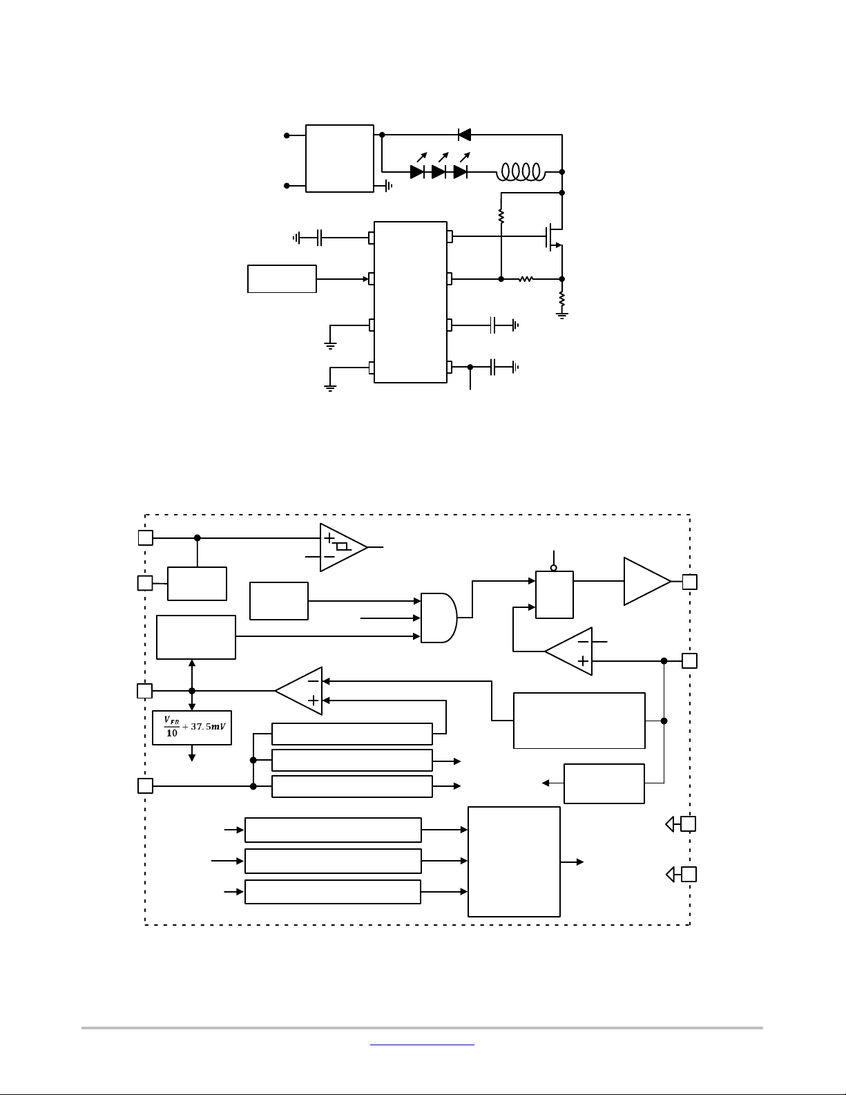
APPLICATION SCHEMATIC
200~500 Vin
VDD
BIAS
FB
3.3 V
LDO
T
OF F.FB
generator
V
FB
V
AC
Dimming
Signal
10 V /
8 V
Soft
Start
OTA
PFC
Stage
FB
DIM
NCL30076
SG
BIAS
PG
External source
Figure 1. Application Schematic
BLOCK DIAGRAM
V
DD−ON
V
TO FF.SS
V
TO FF.ZCD
V
TO FF.FB
V
LED
V
REF
Reference control
DRV
CSZCD
VDD
|| V
V
PDIM
V
ON
S
V
OF F
R
Precise LED
current calculator
RCS
SHUTDOWN
Q
V
PWM
V
CS.LIM
DRV
CSZCD
DIM
V
V
CSZCD
CS.LIM
PWM dimming control
Standby mode control
V
DD
Over voltage protection
Over current protection
T
J
Thermal Shutdown
V
PDIM
V
SHUTDOWN
Protection
AR control
V
TO FF.ZCD
ZCD
detector
V
SHUTDOWN
PG
SG
Figure 2. Simplified Block Diagram
www.onsemi.com
2
NCL30076
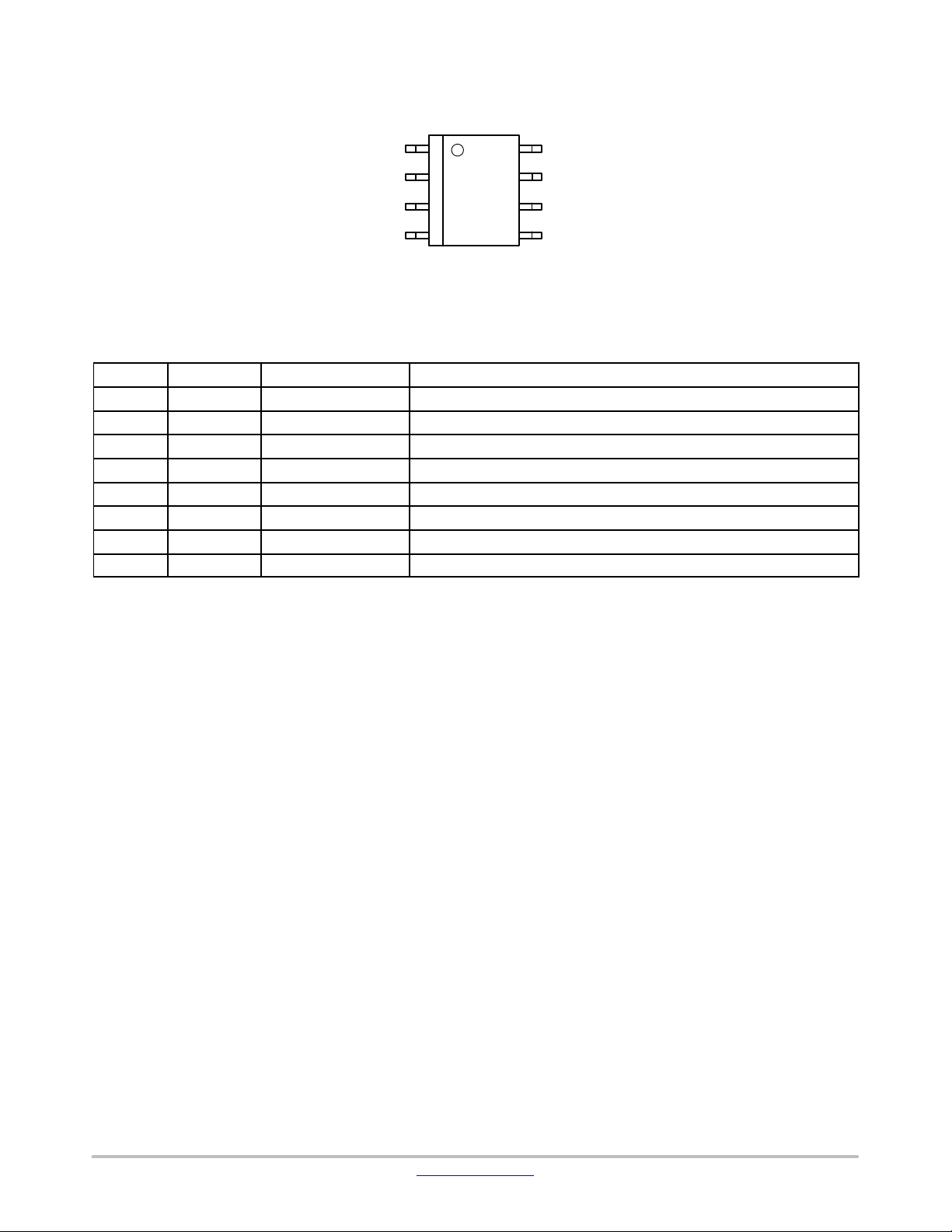
PIN FUNCTION DESCRIPTION
Pin No.
Pin Name
Function
Description
1
BIAS
3.3 V BIAS
This pin is 3.3 V LDO output to bias the internal digital circuit
2
CSZCD
CS and ZCD Sensing
This pin detects the switch current and the inductor current zero cross time
3SGSignal Ground
Signal Ground is close to control pin circuit such as CSZCD, DIM and FB
4FBFeedback
Output of feedback OTA
5
DIM
Dimming Input
Dimming signal is provided to this pin
6
VDD
Power Supply
IC operating current is supplied to this pin
7
DRV
Output Drive
This pin is connected to drive external switch
8PGPower Ground
Power Ground is close to the capacitors at BIAS and VDD pin
PIN CONFIGURATION
(Top View)
Figure 3. Pin Configuration
PGBIAS
DRVCSZCD
VDDSG
DIMFB
www.onsemi.com
3
NCL30076
MAXIMUM RATINGS
Parameter
Symbol
Value
Unit
VDD, DRV Pin Voltage Range
V
−0.3 to 30
V
DIM, FB, CSZCD, BIAS Pin Voltage Range
V
−0.3 to 5.5
V
Maximum Power Dissipation (TA < 50°C)
P
550
mW
Maximum Junction Temperature
T
150
C
Storage Temperature Range
T
−55 to 150
C
Junction−to−Ambient Thermal Impedance
R
145
C/W
ESD Capability, Human Body Model (Note 2)
ESD
2
kV
ESD Capability, Charged Device Model (Note 2)
ESD
1
kV
RECOMMENDED OPERATING RANGES
Parameter
Symbol
Min
Max
Unit
Junction Temperature
TJ−40
125
C
ELECTRICAL CHARACTERISTICS (V
= 15 V and TJ = −40~125°C unless otherwise specified)
Parameter
Test Conditions
Symbol
Min
Typ
Max
Unit
VDD SECTION
IC Turn−On Threshold Voltage
V
9.3
10.0
10.7
V
IC Turn−Off Threshold Voltage
V
7.4
8.0
8.6
V
Startup Current
VDD = V
− 1.6 V
I
−
250
400
A
Operating Current
I
−
6.5
8.0
mA
Standby Current
I
−
200
300
A
BIAS SECTION
3.23
3.30
3.37
TJ = 25~100°C (Note 4)
3.25
3.30
3.35
DIM SECTION
DIM Voltage for 100% V
V
= 1.9 V
V
)
1.755
1.80
1.845
V
DIM Voltage for 99% V
V
)
1.730
1.78
1.827
V
Standby Enabling DIM Voltage
V
5075100
mV
Standby Disabling DIM Voltage
V
60
100
140
mV
Standby Delay Time
t
91011
ms
SPECIFICATIONS
MV(MAX)
LV(MAX)
D(MAX)
J(max)
STG
θJA
HBM
CDM
Stresses exceeding those listed in the Maximum Ratings table may damage the device. If any of these limits are exceeded, device functionality
should not be assumed, damage may occur and reliability may be affected.
1. Refer to ELECTRICAL CHARACTERISTICS, RECOMMENDED OPERATING RANGES and/or APPLICATION INFORMATION for Safe
Operating parameters.
2. This device series incorporates ESD protection and is tested by the following methods:
− ESD Human Body Model per JEDEC Standard JESD22−A114
− ESD Charged Device Model per JEDEC Standard JESD22−C101
− Latch−up Current Maximum Rating ±100 mA per JEDEC Standard JESD78
°
°
°
°
Functional operation above the stresses listed in the Recommended Operating Ranges is not implied. Extended exposure to stresses beyond
the Recommended Operating Ranges limits may affect device reliability.
DD
DD(ON)
DD(OFF)
DD(ON)
BIAS Voltage V
REF
REF
DIM
DIM(REF−MAX
DIM(MAX−EFF
DIM(SB−ENA)
DIM(SB−DIS)
SB(DELAY)
DD(ST)
DD(OP)
DD(SB)
BIAS
m
m
V
www.onsemi.com
4
NCL30076
E
FB SECTION
FB OTA Source Current
IFB = (V
− V
) x g
x 10
I
−14.0
−11.5
−9.0
A
FB OTA Sink Current
IFB = (V
− V
) x g
x 10
I
9.0
11.5
14.0
A
FB OTA Transconductance
g
= IFB / {(V
− V
) x 10}
g
182328
mho
FB OTA High Voltage
V
= 150 mV, V
= 100 mV
V
4.7−−
V
FB Minimum Clamping Voltage
V
= 0 mV, V
= 100 mV
V
0.4
0.5
0.6
V
CS SECTION
CS Regulation
V
)
155
160
165
mV
CS Current Limit Maximum
V
390
410
430
mV
CS Current Limit Minimum
V
145
155
165
mV
DUTY SECTION
Leading Edge Blanking Time at
t
360
400
440
ns
Maximum Ton Time
t
455055
s
Minimum Toff Time
VFB = 3.8 V
t
900
1250
1500
ns
Maximum Toff Time
VFB = 0.5 V
t
1.17
1.30
1.43
ms
Maximum FB Voltage for Min. Toff
V
)
3.30
3.43
3.55
V
Minimum FB Voltage for Max. Toff
V
)
0.9
1.1
1.3
V
Quasi−Resonant Delay Time
tQR0.45
0.50
0.55
s
DRV SECTION
DRV Low Voltage
V
−−0.2
V
DRV High Voltage
VDD = 15 V
V
111213
V
DRV Rising Time
C
= 3.3 nF
t
60
100
145
ns
DRV Falling Time
C
= 3.3 nF
t
2555105
ns
AUTO RESTART SECTION
Auto Restart Time at Protection
t
0.9
1.0
1.1
s
VDD OVER VOLTAGE PROTECTION SECTION
VDD Over Voltage Threshold Voltage
V
222324
V
OVER CURRENT PROTECTION SECTION
CS Over Current Protection
V
0.9
1.0
1.1
V
THERMAL SHUTDOWN SECTION
Thermal Shut Down Temperature
TSD130
150
170°C
Thermal Shut Down Hysteresis
T
253035°C
LECTRICAL CHARACTERISTICS (V
Parameter UnitMaxTypMinSymbolTest Conditions
Turn−on
= 15 V and TJ = −40~125°C unless otherwise specified) (continued)
DD
LED
REF
V
= 150 mV, V
REF
V
= 50 mV, V
REF
M(FB)
REF
REF
LED
LED
REF
LED
REF
LED
LED
M(FB)
= 100 mV
M(FB)
= 100 mV
LED
FB(SOURCE)
FB(SINK)
M(FB)
FB(HIGH)
FB(CLP)
CS(REG−MAX
CS(LIM−MAX)
CS(LIM−MIN)
LEB(TON)
ON(MAX)
OFF(MIN)
OFF(MAX)
FB(MAX−TOFF
FB(MIN−TOFF
m
m
m
m
m
DRV(LOW)
DRV(HIGH)
DRV
DRV
Threshold
DRV(R)
DRV(F)
AR(PROT)
DD(OVP)
CS(OCP)
(Note 3)
(Note 3)
SD(HYS)
Product parametric performance is indicated in the Electrical Characteristics for the listed test conditions, unless otherwise noted. Product
performance may not be indicated by the Electrical Characteristics if operated under different conditions.
3. Guaranteed by design.
4. Guaranteed by characterization.
www.onsemi.com
5
 Loading...