

Page 1
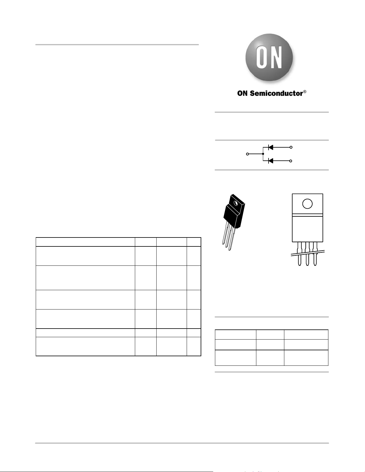
MURF1660CT
Preferred Device
SWITCHMODEt
Power Rectifier
These state-of-the-art devices are designed for use in switching
power supplies, inverters and as free wheeling diodes.
Features
•Ultrafast 60 Nanosecond Recovery Times
•150°C Operating Junction Temperature
•Epoxy Meets UL 94 V-0 @ 0.125 in
•High Temperature Glass Passivated Junction
•Low Leakage Specified @ 150°C Case Temperature
•Current Derating @ Both Case and Ambient Temperatures
•Electrically Isolated. No Isolation Hardware Required.
•Pb-Free Package is Available*
Mechanical Characteristics:
•Case: Epoxy, Molded
•Weight: 1.9 Grams (Approximately)
•Finish: All External Surfaces Corrosion Resistant and Terminal
Leads are Readily Solderable
•Lead Temperature for Soldering Purposes: 260°C Max. for 10 Seconds
MAXIMUM RATINGS (Per Leg)
Rating
Peak Repetitive Reverse Voltage
Working Peak Reverse Voltage
DC Blocking Voltage
Average Rectified Forward Current
Total Device, (Rated V
Per Diode
Per Device
Peak Repetitive Forward Current
(Rated V
TC = 150°C
Non-repetitive Peak Surge Current
(Surge applied at rated load conditions
halfwave, single phase, 60 Hz)
Operating Junction and Storage Temperature TJ, T
RMS Isolation Voltage
(t = 0.3 second, R.H. ≤ 30%, T
(Note 1) Per Figure 3
Stresses exceeding Maximum Ratings may damage the device. Maximum
Ratings are stress ratings only. Functional operation above the Recommended
Operating Conditions is not implied. Extended exposure to stresses above the
Recommended Operating Conditions may affect device reliability.
1. Proper strike and creepage distance must be provided.
, Square Wave, 20 kHz),
R
), TC = 150°C
R
= 25°C)
A
Symbol Value Unit
V
V
I
F(AV)
I
V
RRM
RWM
V
R
I
FM
FSM
iso1
stg
600 V
A
8
16
16 A
100 A
- 65 to +150 °C
V
4500
http://onsemi.com
ULTRAFAST RECTIFIER
16 AMPERES, 600 VOLTS
1
2
3
MARKING
DIAGRAM
AYWW
U1660G
ISOLATED TO-220
CASE 221D
1
2
3
STYLE 3
A = Assembly Location
Y = Year
WW = Work Week
U1660 = Device Code
G = Pb-Free Package
AKA = Diode Polarity
ORDERING INFORMATION
Device Package Shipping
MURF1660CT TO-220 50 Units/Rail
MURF1660CTG TO-220
Preferred devices are recommended choices for future use
and best overall value.
(Pb-Free)
A K A
50 Units/Rail
*For additional information on our Pb-Free strategy and soldering details, please
download the ON Semiconductor Soldering and Mounting Techniques
Reference Manual, SOLDERRM/D.
© Semiconductor Components Industries, LLC, 2007
June, 2007 - Rev. 5
1 Publication Order Number:
MURF1660CT/D
Page 2
MURF1660CT
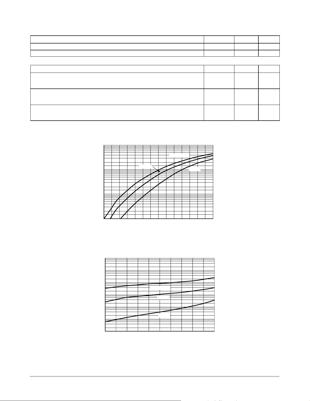
THERMAL CHARACTERISTICS (Per Leg)
Characteristic
Maximum Thermal Resistance, Junction-to-Case
Lead Temperature for Soldering Purposes: 1/8″ from Case for 5 Seconds T
ELECTRICAL CHARACTERISTICS (Per Leg)
Characteristic
Maximum Instantaneous Forward Voltage (Note 2)
(i
= 8.0 A, TC = 150°C)
F
(iF = 8.0 A, TC = 25°C)
Maximum Instantaneous Reverse Current (Note 2)
(Rated DC Voltage, TC = 150°C)
(Rated DC Voltage, TC = 25°C)
Maximum Reverse Recovery Time
= 1.0 A, di/dt = 50 A/ms)
(I
F
= 0.5 A, iR = 1.0 A, I
(I
F
2. Pulse Test: Pulse Width = 300 ms, Duty Cycle ≤ 2.0%.
= 0.25 A)
REC
100
50
20
100°C
10
TJ = 150°C
25°C
5
Symbol Value Unit
R
q
JC
L
3.0 °C/W
260 °C
Symbol Value Unit
v
F
1.20
V
1.50
i
R
500
mA
10
t
rr
60
ns
50
2
1
0.5
0.2
0.1
, INSTANTANEOUS FORWARD CURRENT (AMPS)
F
0.4 0.6 1.0 1.2 1.6 1.8
i
0.8 1.4
v
, INSTANTANEOUS VOLTAGE (V)
F
Figure 1. Typical Forward Voltage, Per Leg
10 K
1.0 K
, REVERSE CURRENT (A)μ
R
I
0.01
100
10
1.0
0.1
TJ = 150°C
100°C
25°C
VR, REVERSE VOLTAGE (V)
600500400300200100
Figure 2. Typical Reverse Current, Per Leg*
http://onsemi.com
2
Page 3

MURF1660CT
TEST CONDITION FOR ISOLATION TEST*
FULLY ISOLATED PACKAGE
LEADS
HEATSINK
0.110, MIN
Figure 3. Mounting Position
* Measurement made between leads and heatsink with all leads shorted together.
MOUNTING INFORMATION
CLIP
HEATSINK
Clip-Mounted
Figure 4. Typical Mounting Technique
http://onsemi.com
3
Page 4
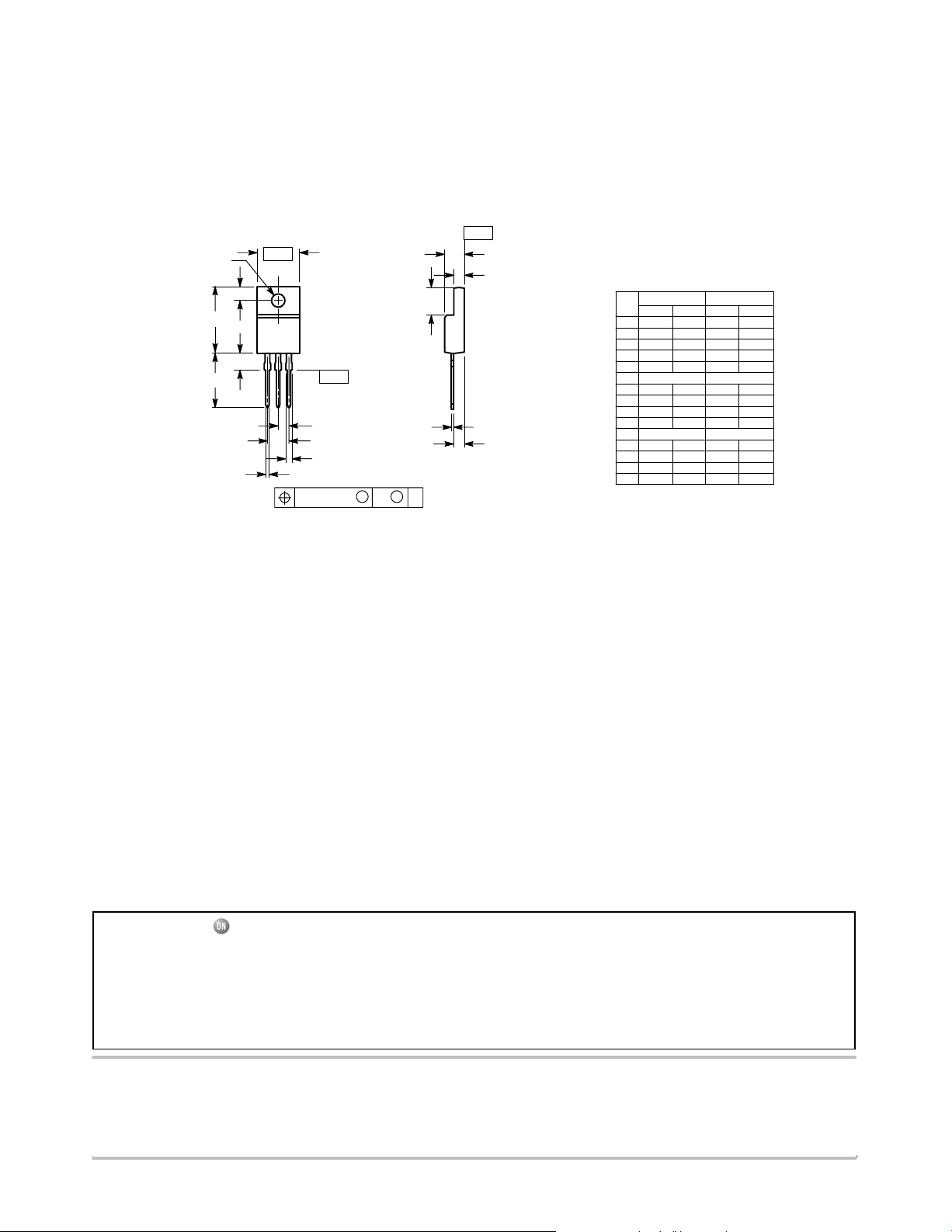
MURF1660CT
PACKAGE DIMENSIONS
TO-220 FULLPAK
CASE 221D-03
ISSUE J
SEATING
-T-
PLANE
F
-B-
Q
C
S
U
A
123
H
K
-Y-
G
N
J
R
L
D
3 PL
M
M
0.25 (0.010) Y
B
NOTES:
1. DIMENSIONING AND TOLERANCING PER ANSI
Y14.5M, 1982.
2. CONTROLLING DIMENSION: INCH
3. 221D-01 THRU 221D-02 OBSOLETE, NEW
STANDARD 221D-03.
INCHES
DIMAMIN MAX MIN MAX
0.617 0.635 15.67 16.12
B 0.392 0.419 9.96 10.63
C 0.177 0.193 4.50 4.90
D 0.024 0.039 0.60 1.00
F 0.116 0.129 2.95 3.28
G 0.100 BSC 2.54 BSC
H 0.118 0.135 3.00 3.43
J 0.018 0.025 0.45 0.63
K 0.503 0.541 12.78 13.73
L 0.048 0.058 1.23 1.47
N 0.200 BSC 5.08 BSC
Q 0.122 0.138 3.10 3.50
R 0.099 0.117 2.51 2.96
S 0.092 0.113 2.34 2.87
U 0.239 0.271 6.06 6.88
STYLE 3:
PIN 1. ANODE
2. CATHODE
3. ANODE
MILLIMETERS
SWITCHMODE is a trademark of Semiconductor Components Industries, LLC.
ON Semiconductor and are registered trademarks of Semiconductor Components Industries, LLC (SCILLC). SCILLC reserves the right to make changes without further notice
to any products herein. SCILLC makes no warranty, representation or guarantee regarding the suitability of its products for any particular purpose, nor does SCILLC assume any liability
arising out of the application or use of any product or circuit, and specifically disclaims any and all liability, including without limitation special, consequential or incidental damages.
“Typical” parameters which may be provided in SCILLC data sheets and/or specifications can and do vary in different applications and actual performance may vary over time. All
operating parameters, including “Typicals” must be validated for each customer application by customer's technical experts. SCILLC does not convey any license under its patent rights
nor the rights of others. SCILLC products are not designed, intended, or authorized for use as components in systems intended for surgical implant into the body, or other applications
intended to support or sustain life, or for any other application in which the failure of the SCILLC product could create a situation where personal injury or death may occur. Should
Buyer purchase or use SCILLC products for any such unintended or unauthorized application, Buyer shall indemnify and hold SCILLC and its officers, employees, subsidiaries, affiliates,
and distributors harmless against all claims, costs, damages, and expenses, and reasonable attorney fees arising out of, directly or indirectly, any claim of personal injury or death
associated with such unintended or unauthorized use, even if such claim alleges that SCILLC was negligent regarding the design or manufacture of the part. SCILLC is an Equal
Opportunity/Affirmative Action Employer. This literature is subject to all applicable copyright laws and is not for resale in any manner.
PUBLICATION ORDERING INFORMATION
LITERATURE FULFILLMENT:
Literature Distribution Center for ON Semiconductor
P.O. Box 5163, Denver, Colorado 80217 USA
Phone: 303-675-2175 or 800-344-3860 Toll Free USA/Canada
Fax: 303-675-2176 or 800-344-3867 Toll Free USA/Canada
Email: orderlit@onsemi.com
N. American Technical Support: 800-282-9855 Toll Free
USA/Canada
Europe, Middle East and Africa Technical Support:
Phone: 421 33 790 2910
Japan Customer Focus Center
Phone: 81-3-5773-3850
http://onsemi.com
ON Semiconductor Website: www.onsemi.com
Order Literature: http://www.onsemi.com/orderlit
For additional information, please contact your local
Sales Representative
MURF1660CT/D
4
 Loading...