

MUN5111T1 Series
Preferred Devices
Bias Resistor Transistor
PNP Silicon Surface Mount Transistor
with Monolithic Bias Resistor Network
This new series of digital transistors is designed to replace a single
device and its external resistor bias network. The Bias Resistor
Transistor (BRT) contains a single transistor with a monolithic bias
network consisting of two resistors; a series base resistor and a
base−emitter resistor. The BRT eliminates these individual
components by integrating them into a single device. The use of a BRT
can reduce both system cost and board space. The device is housed in
the SC−70/SOT−323 package which is designed for low power
surface mount applications.
Features
• Pb−Free Packages are Available
• Simplifies Circuit Design
• Reduces Board Space
• Reduces Component Count
• The SC−70/SOT−323 package can be soldered using wave or reflow.
The modified gull−winged leads absorb thermal stress during
soldering eliminating the possibility of damage to the die.
• Available in 8 mm embossed tape and reel − Use the Device Number
to order the 7 inch/3000 unit reel. Replace “T1” with “T3” in the
Device Number to order the 13 inch/10,000 unit reel.
MAXIMUM RATINGS (T
Rating Symbol Value Unit
Collector-Base Voltage V
Collector-Emitter Voltage V
Collector Current I
Maximum ratings are those values beyond which device damage can occur.
Maximum ratings applied to the device are individual stress limit values (not
normal operating conditions) and are not valid simultaneously. If these limits
are exceeded, device functional operation is not implied, damage may occur
and reliability may be affected.
THERMAL CHARACTERISTICS
Characteristic Symbol Max Unit
Total Device Dissipation
T
= 25°C
A
Derate above 25°C
Thermal Resistance, Junction-to-Ambient R
Thermal Resistance, Junction-to-Lead R
Junction and Storage Temperature Range TJ, T
1. FR−4 @ Minimum Pad
2. FR−4 @ 1.0 x 1.0 inch Pad
= 25°C unless otherwise noted)
A
CBO
CEO
C
P
D
JA
JL
stg
50 Vdc
50 Vdc
100 mAdc
202 (Note 1)
310 (Note 2)
1.6 (Note 1)
2.5 (Note 2)
618 (Note 1)
403 (Note 2)
280 (Note 1)
332 (Note 2)
−55 to +150 °C
mW
°C/W
°C/W
°C/W
http://onsemi.com
PNP SILICON
BIAS RESISTOR
TRANSISTORS
PIN 3
PIN 1
BASE
(INPUT)
R
1
R
2
1
2
SC−70/SOT−323
CASE 419
STYLE 3
MARKING DIAGRAM
6x M
6x = Specific Device Code
M = Date Code
(See Order Info Table)
ORDERING INFORMATION
See specific ordering and shipping information in the package
dimensions section on page 2 of this data sheet.
Preferred devices are recommended choices for future use
and best overall value.
COLLECTOR
(OUTPUT)
PIN 2
EMITTER
(GROUND)
3
Semiconductor Components Industries, LLC, 2004
October, 2004 − Rev. 7
1 Publication Order Number:
MUN5111T1/D
MUN5111T1 Series
ORDERING INFORMATION AND RESISTOR VALUES
Device Package Marking R1 (K) R2 (K) Shipping
MUN5111T1 SC−70/SOT−323 6A 10 10 3000/Tape & Reel
MUN5111T1G SC−70/SOT−323
MUN5112T1 SC−70/SOT−323 6B 22 22 3000/Tape & Reel
MUN5112T1G SC−70/SOT−323
MUN5113T1
MUN5113T3
MUN5113T1G SC−70/SOT−323
MUN5114T1 SC−70/SOT−323 6D 10 47 3000/Tape & Reel
MUN5114T1G SC−70/SOT−323
MUN5115T1 (Note 3) SC−70/SOT−323 6E 10 ∞ 3000/Tape & Reel
MUN5115T1G (Note 3) SC−70/SOT−323
MUN5116T1 (Note 3) SC−70/SOT−323 6F 4.7 ∞ 3000/Tape & Reel
MUN5130T1 (Note 3) SC−70/SOT−323 6G 1.0 1.0 3000/Tape & Reel
MUN5130T1G (Note 3) SC−70/SOT−323
MUN5131T1 (Note 3) SC−70/SOT−323 6H 2.2 2.2 3000/Tape & Reel
MUN5131T1G (Note 3) SC−70/SOT−323
MUN5132T1 (Note 3) SC−70/SOT−323 6J 4.7 4.7 3000/Tape & Reel
MUN5132T1G (Note 3) SC−70/SOT−323
MUN5133T1 (Note 3) SC−70/SOT−323 6K 4.7 47 3000/Tape & Reel
MUN5133T1G (Note 3) SC−70/SOT−323
MUN5134T1 (Note 3) SC−70/SOT−323 6L 22 47 3000/Tape & Reel
MUN5135T1 (Note 3) SC−70/SOT−323 6M 2.2 47 3000/Tape & Reel
MUN5136T1 SC−70/SOT−323 6N 100 100 3000/Tape & Reel
MUN5137T1 SC−70/SOT−323 6P 47 22 3000/Tape & Reel
†For information on tape and reel specifications, including part orientation and tape sizes, please refer to our Tape and Reel Packaging
Specifications Brochure, BRD8011/D.
3. New devices. Updated curves to follow in subsequent data sheets.
(Pb−Free)
(Pb−Free)
SC−70/SOT−323 6C 47 47 3000/Tape & Reel
(Pb−Free)
(Pb−Free)
(Pb−Free)
(Pb−Free)
(Pb−Free)
(Pb−Free)
(Pb−Free)
6A 10 10 3000/Tape & Reel
6B 22 22 3000/Tape & Reel
10,000/Tape & Reel
6C 47 47 3000/Tape & Reel
6D 10 47 3000/Tape & Reel
6E 10 ∞ 3000/Tape & Reel
6G 1.0 1.0 3000/Tape & Reel
6H 2.2 2.2 3000/Tape & Reel
6J 4.7 4.7 3000/Tape & Reel
6K 4.7 47 3000/Tape & Reel
†
http://onsemi.com
2
MUN5111T1 Series
ELECTRICAL CHARACTERISTICS (T
= 25°C unless otherwise noted)
A
Characteristic
OFF CHARACTERISTICS
Collector−Base Cutoff Current (VCB = 50 V, IE = 0) I
Collector−Emitter Cutoff Current (VCE = 50 V, IB = 0) I
Emitter−Base Cutoff Current MUN5111T1
(V
= 6.0 V, IC = 0) MUN5112T1
EB
MUN5113T1
MUN5114T1
MUN5115T1
MUN5116T1
MUN5130T1
MUN5131T1
MUN5132T1
MUN5133T1
MUN5134T1
MUN5135T1
MUN5136T1
MUN5137T1
Collector−Base Breakdown Voltage (IC = 10 A, IE = 0) V
Collector−Emitter Breakdown Voltage (Note 4)
= 2.0 mA, IB = 0)
(I
C
ON CHARACTERISTICS (Note 4)
DC Current Gain MUN5111T1
(V
= 10 V, IC = 5.0 mA) MUN5112T1
CE
Collector−Emitter Saturation Voltage (IC = 10 mA, IE = 0.3 mA)
(I
= 10 mA, IB = 5 mA) MUN5130T1/MUN5131T1
C
= 10 mA, IB = 1 mA) MUN5115T1/MUN5116T1/
(I
C
MUN5132T1/MUN5133T1/MUN5134T1
Output Voltage (on)
(V
= 5.0 V, VB = 2.5 V, RL = 1.0 k) MUN5111T1
CC
(V
= 5.0 V, VB = 3.5 V, RL = 1.0 k) MUN5113T1
CC
(V
= 5.0 V, VB = 5.5 V, RL = 1.0 k) MUN5136T1
CC
= 5.0 V, VB = 4.0 V, RL = 1.0 k) MUN5137T1
(V
CC
4. Pulse Test: Pulse Width < 300 s, Duty Cycle < 2.0%
MUN5113T1
MUN5114T1
MUN5115T1
MUN5116T1
MUN5130T1
MUN5131T1
MUN5132T1
MUN5133T1
MUN5134T1
MUN5135T1
MUN5136T1
MUN5137T1
MUN5112T1
MUN5114T1
MUN5115T1
MUN5116T1
MUN5130T1
MUN5131T1
MUN5132T1
MUN5133T1
MUN5134T1
MUN5135T1
Symbol Min Typ Max Unit
CBO
CEO
I
EBO
(BR)CBO
V
(BR)CEO
h
V
CE(sat)
V
FE
OL
− − 100 nAdc
− − 500 nAdc
−
−
−
−
−
−
−
−
−
−
−
−
−
−
−
−
−
−
−
−
−
−
−
−
−
−
−
−
0.5
0.2
0.1
0.2
0.9
1.9
4.3
2.3
1.5
0.18
0.13
0.2
0.05
0.13
mAdc
50 − − Vdc
50 − − Vdc
35
60
80
80
160
160
3.0
8.0
15
80
80
80
80
80
60
100
140
140
250
250
5.0
15
27
140
130
140
150
140
−
−
−
−
−
−
−
−
−
−
−
−
−
−
− − 0.25 Vdc
−
−
−
−
−
−
−
−
−
−
−
−
−
−
−
−
−
−
−
−
−
−
−
−
−
−
−
−
0.2
0.2
0.2
0.2
0.2
0.2
0.2
0.2
0.2
0.2
0.2
0.2
0.2
0.2
Vdc
http://onsemi.com
3
MUN5111T1 Series
ELECTRICAL CHARACTERISTICS (T
= 25°C unless otherwise noted) (Continued)
A
Characteristic
Output Voltage (off) (VCC = 5.0 V, VB = 0.5 V, RL = 1.0 k)
(V
= 5.0 V, VB = 0.050 V, RL = 1.0 k) MUN5130T1
CC
= 5.0 V, VB = 0.25 V, RL = 1.0 k) MUN5115T1
(V
CC
MUN5116T1
MUN5131T1
MUN5132T1
Input Resistor MUN5111T1
MUN5112T1
MUN5113T1
MUN5114T1
MUN5115T1
MUN5116T1
MUN5130T1
MUN5131T1
MUN5132T1
MUN5133T1
MUN5134T1
MUN5135T1
MUN5136T1
MUN5137T1
Resistor Ratio MUN5111T1/MUN5112T1/MUN5113T1/
MUN5136T1
MUN5114T1
MUN5115T1/MUN5116T1
MUN5130T1/MUN5131T1/MUN5132T1
MUN5133T1
MUN5134T1
MUN5135T1
MUN5137T1
Symbol Min Typ Max Unit
V
OH
R1 7.0
R1/R
2
4.9 − − Vdc
15.4
32.9
7.0
7.0
3.3
0.7
1.5
3.3
3.3
15.4
1.54
70
32.9
0.8
0.17
−
0.8
0.055
0.38
0.038
1.7
10
22
47
10
10
4.7
1.0
2.2
4.7
4.7
22
2.2
100
47
1.0
0.21
−
1.0
0.1
0.47
0.047
2.1
13
28.6
61.1
13
13
6.1
1.3
2.9
6.1
6.1
28.6
2.86
130
61.1
1.2
0.25
−
1.2
0.185
0.56
0.056
2.6
k
250
200
150
100
R
= 833°C/W
50
, POWER DISSIPATION (MILLIWATTS)
D
P
0
−50 0 50 100 150
JA
T
, AMBIENT TEMPERATURE (°C)
A
Figure 1. Derating Curve
http://onsemi.com
4

MUN5111T1 Series
TYPICAL ELECTRICAL CHARACTERISTICS − MUN5111T1
1
IC/IB = 10
0.1
, MAXIMUM COLLECTOR VOLTAGE (VOLTS)
0.01
CE(sat)
V
0 40
20
, COLLECTOR CURRENT (mA)
I
C
Figure 2. V
CE(sat)
4
3
2
T
=−25°C
A
75°C
versus I
C
f = 1 MHz
l
= 0 V
E
T
= 25°C
A
25°C
, DC CURRENT GAIN (NORMALIZED)
FE
50
1000
VCE = 10 V
T
100
10
1 10 100
IC, COLLECTOR CURRENT (mA)
Figure 3. DC Current Gain
100
75°C
10
1
25°C
T
=−25°C
A
=75°C
A
25°C
−25°C
, CAPACITANCE (pF)
ob
1
C
0
010203040
, REVERSE BIAS VOLTAGE (VOLTS)
V
R
Figure 4. Output Capacitance Figure 5. Output Current versus Input Voltage
100
VO = 0.2 V
10
1
, INPUT VOLTAGE (VOLTS)
in
V
0.1
0
10 20 30 40 50
Figure 6. Input Voltage versus Output Current
0.1
, COLLECTOR CURRENT (mA) h
C
0.01
I
0.001
50
T
=−25°C
A
75°C
, COLLECTOR CURRENT (mA)
I
C
0
1 2 3 4 5
25°C
VO = 5 V
6 7 8 9 10
Vin, INPUT VOLTAGE (VOLTS)
http://onsemi.com
5

MUN5111T1 Series
TYPICAL ELECTRICAL CHARACTERISTICS − MUN5112T1
10
IC/IB = 10
1
T
=−25°C
A
0.1
, MAXIMUM COLLECTOR VOLTAGE (VOLTS)
0.01
CE(sat)
V
0 20 50
I
, COLLECTOR CURRENT (mA)
C
Figure 7. V
CE(sat)
versus I
C
4
3
2
25°C
75°C
40
f = 1 MHz
= 0 V
l
E
T
= 25°C
A
1000
100
, DC CURRENT GAIN (NORMALIZED)
FE
10
1
100
75°C
10
1
10
I
, COLLECTOR CURRENT (mA)
C
Figure 8. DC Current Gain
25°C
T
=−25°C
A
VCE = 10 V
T
=75°C
A
25°C
−25°C
100
, CAPACITANCE (pF)
ob
1
C
0
010203040
V
, REVERSE BIAS VOLTAGE (VOLTS)
R
Figure 9. Output Capacitance
, INPUT VOLTAGE (VOLTS)
in
V
100
10
0.1
VO = 0.2 V
1
0 10 20 30
0.1
, COLLECTOR CURRENT (mA) h
C
I
0.01
0.001
50
0 1 2 3 4
Figure 10. Output Current versus Input Voltage
T
=−25°C
A
25°C
75°C
IC, COLLECTOR CURRENT (mA)
V
in
40 50
VO = 5 V
5 6 7 8 9 10
, INPUT VOLTAGE (VOLTS)
Figure 11. Input Voltage versus Output Current
http://onsemi.com
6

MUN5111T1 Series
TYPICAL ELECTRICAL CHARACTERISTICS − MUN5113T1
1
IC/IB = 10
T
=−25°C
A
25°C
75°C
0.1
, MAXIMUM COLLECTOR VOLTAGE (VOLTS)
0.01
CE(sat)
V
010203040
IC, COLLECTOR CURRENT (mA)
Figure 12. V
CE(sat)
versus I
C
1
f = 1 MHz
l
= 0 V
0.8
E
T
A
= 25°C
0.6
1000
T
=75°C
A
100
, DC CURRENT GAIN (NORMALIZED)
FE
10
1 10 100
, COLLECTOR CURRENT (mA)
I
C
Figure 13. DC Current Gain
100
10
1
T
=75°C
A
25°C
−25°C
25°C
−25°C
0.4
, CAPACITANCE (pF)
ob
C
0.2
0
010203040
, REVERSE BIAS VOLTAGE (VOLTS)
V
R
Figure 14. Output Capacitance Figure 15. Output Current versus Input Voltage
100
T
A
10
1
, INPUT VOLTAGE (VOLTS)
in
V
0.1
0 10 20 30 40
0.1
0.01
, COLLECTOR CURRENT (mA) h
C
I
0.001
50
010
=−25°C
25°C
75°C
IC, COLLECTOR CURRENT (mA)
VO = 5 V
123456789
Vin, INPUT VOLTAGE (VOLTS)
VO = 0.2 V
50
Figure 16. Input Voltage versus Output Current
http://onsemi.com
7

MUN5111T1 Series
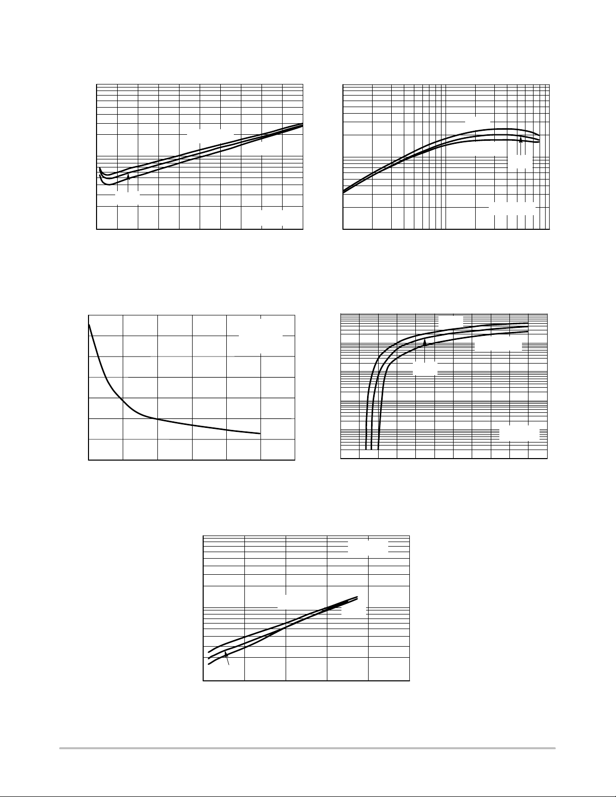
TYPICAL ELECTRICAL CHARACTERISTICS − MUN5114T1
1
IC/IB = 10
0.1
0.01
, MAXIMUM COLLECTOR VOLTAGE (VOLTS)
CE(sat)
0.001
V
020406080
IC, COLLECTOR CURRENT (mA)
Figure 17. V
4.5
4
3.5
3
2.5
2
1.5
, CAPACITANCE (pF)
ob
C
1
0.5
0
0 2 4 6 8101520253035404550
V
, REVERSE BIAS VOLTAGE (VOLTS)
R
CE(sat)
T
=−25°C
A
75°C
versus I
C
f = 1 MHz
l
= 0 V
E
= 25°C
T
A
25°C
Figure 19. Output Capacitance Figure 20. Output Current versus Input Voltage
180
T
=75°C
VCE = 10 V
160
140
120
100
80
60
40
, DC CURRENT GAIN (NORMALIZED)
20
FE
0
2 4 6 8 15 20 40 50 60 70 80 90
1 10 100
IC, COLLECTOR CURRENT (mA)
−25°C
A
25°C
Figure 18. DC Current Gain
100
T
=75°C
A
−25°C
10
, COLLECTOR CURRENT (mA) h
C
I
1
0 246810
Vin, INPUT VOLTAGE (VOLTS)
25°C
VO = 5 V
10
VO = 0.2 V
75°C
1
, INPUT VOLTAGE (VOLTS)
in
V
0.1
010 20 30 4050
IC, COLLECTOR CURRENT (mA)
T
=−25°C
A
25°C
Figure 21. Input Voltage versus Output Current
http://onsemi.com
+12 V
T ypical Application
for PNP BRTs
LOAD
Figure 22. Inexpensive, Unregulated Current Source
8

MUN5111T1 Series
TYPICAL ELECTRICAL CHARACTERISTICS — MUN5132T1
1
0.1
, MAXIMUM COLLECTOR
VOLTAGE (VOLTS)
CE(sat)
V
0.01
10
9
8
7
6
5
4
, CAPACITANCE (pF)
3
ob
C
2
1
0
75°C
25°C
−25°C
I
, COLLECTOR CURRENT (mA)
C
Figure 23. Maximum Collector V oltage versus
Collector Current
1000
, DC CURRENT GAIN
FE
h
35302520151050
100
, COLLECTOR CURRENT (mA)
C
I
6050403020100
0.01
100
10
10
0.1
75°C
−25°C
25°C
1
40 60 80 100
I
, COLLECTOR CURRENT (mA)
C
120200
Figure 24. DC Current Gain
75°C
1
Vin, INPUT VOLTAGE (VOLTS)VR, REVERSE BIAS VOLTAGE (VOLTS)
25°C
−25°C
6543210
10987
Figure 25. Output Capacitance Figure 26. Output Current versus Input Voltage
10
−25°C
25°C
75°C
IC, OUTPUT CURRENT (mA)
302520151050
454035 50
, INPUT VOLTAGE (VOLTS)
in
V
0.1
1
Figure 27. Input Voltage versus Output Current
http://onsemi.com
9

MUN5111T1 Series
TYPICAL ELECTRICAL CHARACTERISTICS — MUN5136T1
, MAXIMUM COLLECTOR
VOLTAGE (VOLTS)
CE(sat)
V
0.01
1.2
1.0
0.8
0.6
1
0.1
−25°C
I
, COLLECTOR CURRENT (mA)
C
Figure 28. Maximum Collector V oltage versus
Collector Current
f = 1 MHz
I
E
T
A
25°C
IC/IB = 10
= 0 V
= 25°C
75°C
1000
75°C
= −25°C
T
100
A
10
, DC CURRENT GAIN (NORMALIZED)
FE
1
h
76543210
I
, COLLECTOR CURRENT (mA)
C
Figure 29. DC Current Gain
100
25°C
10
25°C
VCE = 10 V
75°C
= −25°C
T
A
100101
0.4
, CAPACITANCE (pF)
ob
C
0.2
0
1
, COLLECTOR CURRENT (mA)
C
I
6050403020100
0.1
VO = 5 V
6543210
Vin, INPUT VOLTAGE (VOLTS)VR, REVERSE BIAS VOLTAGE (VOLTS)
Figure 30. Output Capacitance Figure 31. Output Current versus Input Voltage
100
= −25°C
T
A
VO = 0.2 V
121086420
181614 20
, INPUT VOLTAGE (VOLTS)
in
V
10
25°C
75°C
1
IC, COLLECTOR CURRENT (mA)
10987
Figure 32. Input Voltage versus Output Current
http://onsemi.com
10
MUN5111T1 Series
TYPICAL ELECTRICAL CHARACTERISTICS — MUN5137T1
, MAXIMUM COLLECTOR
VOLTAGE (VOLTS)
CE(sat)
V
0.01
1.4
1.2
1.0
0.8
1
TA = −25°C
0.1
25°C
35302520151050
I
, COLLECTOR CURRENT (mA)
C
Figure 33. Maximum Collector V oltage versus
Collector Current
f = 1 MHz
I
E
T
A
75°C
I
C/IB
= 0 V
= 25°C
= 10
1000
100
, DC CURRENT GAIN (NORMALIZED)
FE
10
h
504540
I
, COLLECTOR CURRENT (mA)
C
Figure 34. DC Current Gain
100
10
1
75°C
TA = −25°C
25°C
VCE = 10 V
100101
75°C
TA = −25°C
25°C
0.6
, CAPACITANCE (pF)
0.4
ob
C
0.2
0
0.1
0.01
, COLLECTOR CURRENT (mA)
C
I
0.001
6050403020100
6543210
V
= 5 V
O
10
Vin, INPUT VOLTAGE (VOLTS)VR, REVERSE BIAS VOLTAGE (VOLTS)
Figure 35. Output Capacitance Figure 36. Output Current versus Input Voltage
100
V
= 0.2 V
O
TA = −25°C
75°C
151050
20 25
, INPUT VOLTAGE (VOLTS)
in
V
10
25°C
1
IC, COLLECTOR CURRENT (mA)
11987
Figure 37. Input Voltage versus Output Current
http://onsemi.com
11

MUN5111T1 Series
PACKAGE DIMENSIONS
SC−70/SOT−323
CASE 419−04
ISSUE L
0.05 (0.002)
A
L
3
S
12
G
H
B
D
C
N
SOLDERING FOOTPRINT*
0.50
0.0197
NOTES:
1. DIMENSIONING AND TOLERANCING PER ANSI
Y14.5M, 1982.
2. CONTROLLING DIMENSION: INCH.
DIM MIN MAX MIN MAX
A 0.071 0.087 1.80 2.20
B 0.045 0.053 1.15 1.35
C 0.032 0.040 0.80 1.00
D 0.012 0.016 0.30 0.40
G 0.047 0.055 1.20 1.40
H 0.000 0.004 0.00 0.10
J 0.004 0.010 0.10 0.25
K 0.017 REF 0.425 REF
L 0.026 BSC 0.650 BSC
N 0.028 REF 0.700 REF
S 0.079 0.095 2.00 2.40
J
K
STYLE 3:
PIN 1. BASE
2. EMITTER
3. COLLECTOR
MILLIMETERSINCHES
0.65
0.025
0.65
0.025
0.40
0.0157
1.9
0.0748
SCALE 20:1
mm
inches
*For additional information on our Pb−Free strategy and soldering
details, please download the ON Semiconductor Soldering and
Mounting Techniques Reference Manual, SOLDERRM/D.
ON Semiconductor and are registered trademarks of Semiconductor Components Industries, LLC (SCILLC). SCILLC reserves the right to make changes without further notice
to any products herein. SCILLC makes no warranty, representation or guarantee regarding the suitability of its products for any particular purpose, nor does SCILLC assume any liability
arising out of the application or use of any product or circuit, and specifically disclaims any and all liability, including without limitation special, consequential or incidental damages.
“Typical” parameters which may be provided in SCILLC data sheets and/or specifications can and do vary in different applications and actual performance may vary over time. All
operating parameters, including “Typicals” must be validated for each customer application by customer’s technical experts. SCILLC does not convey any license under its patent rights
nor the rights of others. SCILLC products are not designed, intended, or authorized for use as components in systems intended for surgical implant into the body, or other applications
intended to support or sustain life, or for any other application in which the failure of the SCILLC product could create a situation where personal injury or death may occur. Should
Buyer purchase or use SCILLC products for any such unintended or unauthorized application, Buyer shall indemnify and hold SCILLC and its officers, employees, subsidiaries, affiliates,
and distributors harmless against all claims, costs, damages, and expenses, and reasonable attorney fees arising out of, directly or indirectly, any claim of personal injury or death
associated with such unintended or unauthorized use, even if such claim alleges that SCILLC was negligent regarding the design or manufacture of the part. SCILLC is an Equal
Opportunity/Affirmative Action Employer. This literature is subject to all applicable copyright laws and is not for resale in any manner.
PUBLICATION ORDERING INFORMATION
LITERATURE FULFILLMENT:
Literature Distribution Center for ON Semiconductor
P.O. Box 61312, Phoenix, Arizona 85082−1312 USA
Phone: 480−829−7710 or 800−344−3860 Toll Free USA/Canada
Fax: 480−829−7709 or 800−344−3867 Toll Free USA/Canada
Email: orderlit@onsemi.com
N. American Technical Support: 800−282−9855 Toll Free
USA/Canada
Japan: ON Semiconductor, Japan Customer Focus Center
2−9−1 Kamimeguro, Meguro−ku, Tokyo, Japan 153−0051
Phone: 81−3−5773−3850
http://onsemi.com
ON Semiconductor Website: http://onsemi.com
Order Literature: http://www.onsemi.com/litorder
For additional information, please contact your
local Sales Representative.
MUN5111T1/D
12

WWW.ALLDATASHEET.COM
Copyright © Each Manufacturing Company.
All Datasheets cannot be modified without permission.
This datasheet has been download from :
www.AllDataSheet.com
100% Free DataSheet Search Site.
Free Download.
No Register.
Fast Search System.
www.AllDataSheet.com
 Loading...