

Page 1
© KEMET Electronics Corporation, P.O. Box 5928, Greenville, S.C. 29606, (864) 963-6300 3
MULTILAYER CERAMIC CAPACITORS/AXIAL & RADIAL LEADED
Multilayer ceramic capacitors are available in a
variety of physical sizes and configurations, including
leaded devices and surface mounted chips. Leaded
styles include molded and conformally coated parts
with axial and radial leads. However, the basic
capacitor element is similar for all styles. It is called a
chip and consists of formulated dielectric materials
which have been cast into thin layers, interspersed
with metal electrodes alternately exposed on opposite
edges of the laminated structure.
The entire structure is
fired at high temperature to produce a monolithic
block
which provides high capacitance values in a
small physical volume. After firing, conductive
terminations are applied to opposite ends of the chip to
make contact with the exposed electrodes.
Termination materials and methods vary depending on
the intended use.
TEMPERATURE CHARACTERISTICS
Ceramic dielectric materials can be formulated with
a wide range of characteristics. The EIA standard for
ceramic dielectric capacitors (RS-198) divides ceramic
dielectrics into the following classes:
Class I: Temperature compensating capacitors,
suitable for resonant circuit application or other applications where high Q and stability of capacitance characteristics are required. Class I capacitors have
predictable temperature coefficients and are not
effected by voltage, frequency or time. They are made
from materials which are not ferro-electric, yielding
superior stability but low volumetric efficiency. Class I
capacitors are the most stable type available, but have
the lowest volumetric efficiency.
Class II: Stable capacitors, suitable for bypass
or coupling applications or frequency discriminating
circuits where Q and stability of capacitance characteristics are not of major importance. Class II
capacitors have temperature characteristics of ± 15%
or less. They are made from materials which are
ferro-electric, yielding higher volumetric efficiency but
less stability. Class II capacitors are affected by
temperature, voltage, frequency and time.
Class III: General purpose capacitors, suitable
for by-pass coupling or other applications in which
dielectric losses, high insulation resistance and
stability of capacitance characteristics are of little or
no importance. Class III capacitors are similar to Class
II capacitors except for temperature characteristics,
which are greater than ± 15%. Class III capacitors
have the highest vol
umetric efficiency and poorest
stability of any type.
KEMET leaded ceramic capacitors are offered in
the three most popular temperature characteristics:
C0G: Class I, with a temperature coefficient of 0 ±
30 ppm per degree C over an operating
temperature range of - 55°C to + 125°C (Also
known as “NP0”).
X7R: Class II, with a maximum capacitance
change of ± 15% over an operating temperature
range of - 55°C to + 125°C.
Z5U: Class III, with a maximum capacitance
change of + 22% - 56% over an operating tem-
perature range of + 10°C to + 85°C.
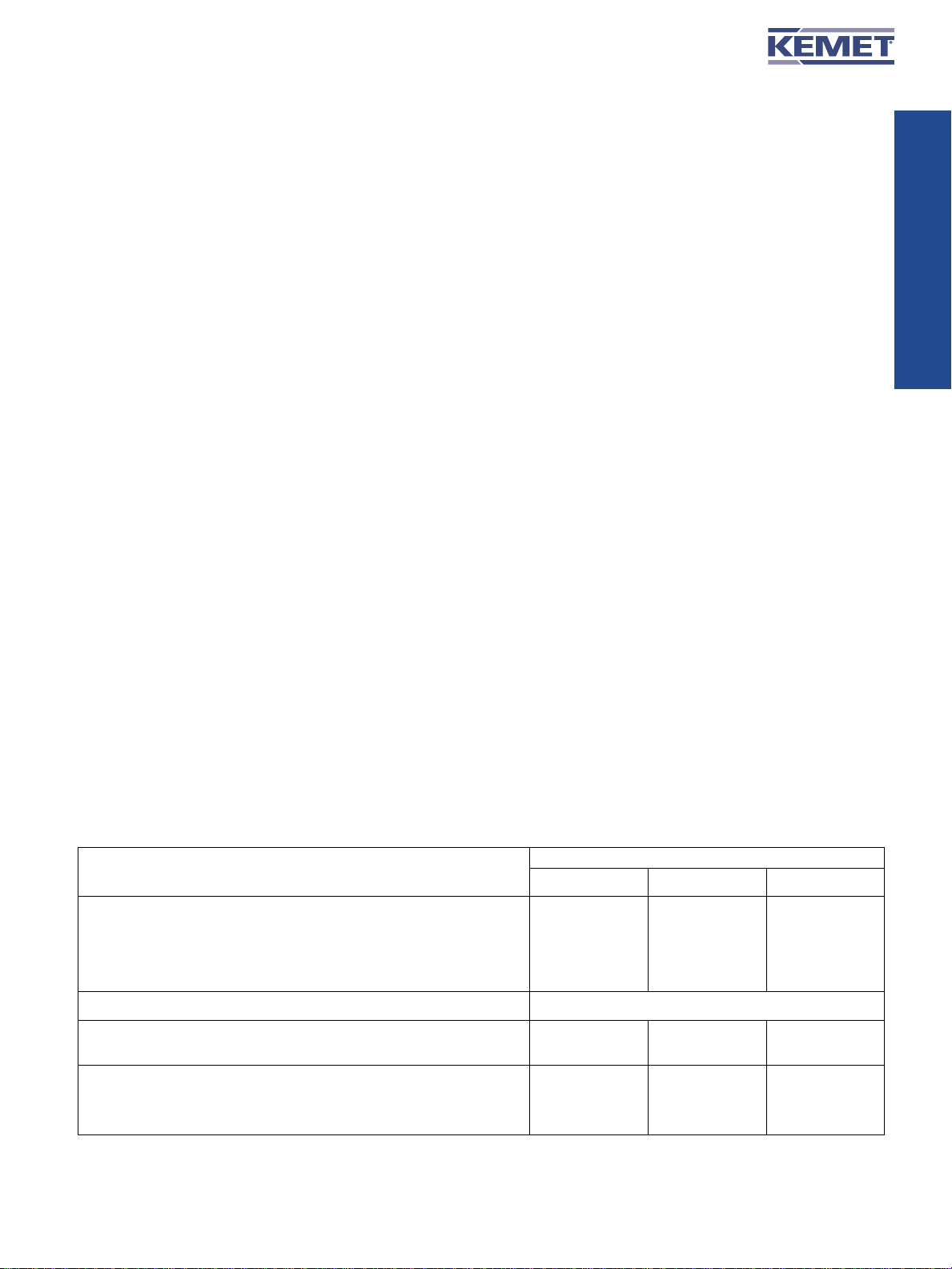
Specified electrical limits for these three temperature
characteristics are shown in Table 1.
SPECIFIED ELECTRICAL LIMITS
TEMPERATURE CHARACTERISTICS
PARAMETER C0G X7R Z5U
Dissipation Factor: Measured at following conditions:
C0G — 1 kHz and 1 vrms if capacitance > 1000 pF
1 MHz and 1 vrms if capacitance ≤ 1000 pF 0.15% 2.5% 4.0%
X7R — 1 kHz and 1 vrms* or if extended cap range 0.5 vrms
Z5U — 1 kHz and 0.5 vrms
Dielectric Strength: 2.5 times rated DC voltage. Pass Subsequent IR Test
Insulation Resistance (IR): At rated DC voltage, 1,000 MΩ-µF 1,000 MΩ-µF 1,000 MΩ-µF
whichever of the two is smaller or 100 GΩ or 100 GΩ or 10 GΩ
Temperature Characteristics: Range, °C -55 to +125 -55 to +125 +10 to +85
Capacitance Change without 0 ± 30 ppm/°C ±15% +22%, -56%
DC voltage
* 1 MHz and 1 vrms if capacitance ≤ 100 pF on military product.
Table I
Multlayer Ceramic
Capacitors
Page 2

CERAMIC CONFORMALLY COATED/AXIAL & RADIAL
PERFORMANCE CHARACTERISTICS FOR STANDARD AND HIGH VOLTAGE
© KEMET Electronics Corporation, P.O. Box 5928, Greenville, S.C. 29606, (864) 963-63004
GENERAL SPECIFICATIONS
Working Voltage:
Axial (WVDC) Radial (WVDC)
C0G – 50 & 100
X7R – 50 & 100
Z5U – 50 & 100 50 & 100
Temperature Characteristics:
C0G – 0 ± 30 PPM / °C from - 55°C to + 125°C (1)
X7R – ± 15% from - 55°C to + 125°C
Z5U – + 22% / -56% from + 10°C to + 85°C
Capacitance Tolerance:
C0G – ±0.5pF, ±1%, ±2%, ±5%, ±10%
X7R – ±10%, ±20%, +80% / -20%, +100% / -0%
Z5U – ±20%, +80% / -20%
Construction:
Epoxy encapsulated - meets flame test requirements of UL
Standard 94V-0.
High-temperature solder - meets EIA RS-198, Method 302,
Condition B (260°C for 10 seconds)
Lead Material:
100% matte tin (Sn) with nickel (Ni) underplate and steel core.
Solderability:
EIA RS-198, Method 301, Solder Temperature: 230°C ±5°C.
Dwell time in solder = 7 ± ½ seconds.
Terminal Strength:
EIA RS-198, Method 303, Condition A (2.2kg)
50, 100, 200, 500, 1k, 1.5k, 2k, 2.5k, 3k
50, 100, 200, 500, 1k, 1.5k, 2k, 2.5k, 3k
ENVIRONMENTAL
Vibration:
EIA RS-198, Method 304, Condition D (10-2000Hz; 20g)
Shock:
EIA RS-198, Method 305, Condition I (100g)
Life Test:
EIA RS-198, Method 201, Condition D.
££
200V
C0G – 200% of rated voltage @ +125°C
X7R – 200% of rated voltage @ +125°C
Z5U – 200% of rated voltage @ +85°C
³³
500V
C0G – rated voltage @ +125°C
X7R – rated voltage @ +125°C
Post Test Limits @ 25°C are:
Capacitance Change:
C0G (£ 200V) – +3% or 0.25pF, whichever is greater.
C0G (³ 500V) – +3% or 0.50pF, whichever is greater.
X7R – + 20% of initial value (2)
Z5U – + 30% of initial value (2)
Dissipation Factor:
C0G – 0.15% maximum
X7R – 2.5% maximum
Z5U – 4.0% maximum
Insulation Resistance:
C0G – 10k Megohm or 100 Megohm x µF, whichever is less.
³1kV tested @ 500V.
X7R – 10k Megohm or 100 Megohm x µF, whichever is less.
³1kV tested @ 500V.
Z5U – 1k Megohm or 100 Megohm x µF, whichever is less.
ELECTRICAL
Capacitance @ 25°C:
Within specified tolerance and following test conditions.
C0G – > 1000pF with 1.0 vrms @ 1 kHz
£ 1000pF with 1.0 vrms @ 1 MHz
X7R – with 1.0 vrms @ 1 kHz
Z5U – with 1.0 vrms @ 1 kHz
Dissipation Factor @ 25°C:
Same test conditions as capacitance.
C0G – 0.15% maximum
X7R – 2.5% maximum
Z5U – 4.0% maximum
Insulation Resistance @ 25°C:
EIA RS-198, Method 104, Condition A <1kV
C0G – 100k Megohm or 1000 Megohm x µF, whichever is less.
£500V test @ rated voltage, ³1kV test @ 500V
X7R – 100k Megohm or 1000 Megohm x µF, whichever is less.
£500V test @ rated voltage, ³1kV test @ 500V
Z5U – 10k Megohm or 1000 Megohm x µF, whichever is less.
Dielectric Withstanding Voltage:
EIA RS-198, Method 103
£200V test @ 250% of rated voltage for 5 seconds with current
limited to 50mA.
500V test @ 150% of rated voltage for 5 seconds with current
limited to 50mA.
³1000V test @ 120% of rated voltage for 5 seconds with current
limited to 50mA.
Moisture Resistance:
EIA RS-198, Method 204, Condition A (10 cycles without
applied voltage.)
Post Test Limits @ 25°C are:
Capacitance Change:
C0G (£ 200V) – +3% or 0.25pF, whichever is greater.
C0G (³ 500V) – +3% or 0.50pF, whichever is greater.
X7R – + 20% of initial value (2)
Z5U – + 30% of initial value (2)
Dissipation Factor:
C0G – 0.25% maximum
X7R – 3.0% maximum
Z5U – 4.0% maximum
Insulation Resistance:
C0G – 10k Megohm or 100 Megohm x µF, whichever is less.
£500V test @ rated voltage, ³1kV test @ 500V.
X7R – 10k Megohm or 100 Megohm x µF, whichever is less.
³500V test @ rated voltage, >1kV test @ 500V.
Z5U – 1k Megohm or 100 Megohm x µF, whichever is less.
Thermal Shock:
EIA RS-198, Method 202, Condition B (C0G & X7R: -55°C to
+125°C); Condition A (Z5U: -55°C to 85°C)
(1) +53 PPM -30 PPM/ °C from +25°C to -55°C, + 60 PPM below
10pF.
(2) X7R and Z5U dielectrics exhibit aging characteristics; there-
fore, it is highly recommended that capacitors be deaged for 2
hours at 150°C and stabilized at room temperature for 48
hours before capacitance measurements are made.
Page 3
CERAMIC CONFORMALLY COATED/RADIAL
“STANDARD & HIGH VOLTAGE GOLDEN MAX”
Golden Max
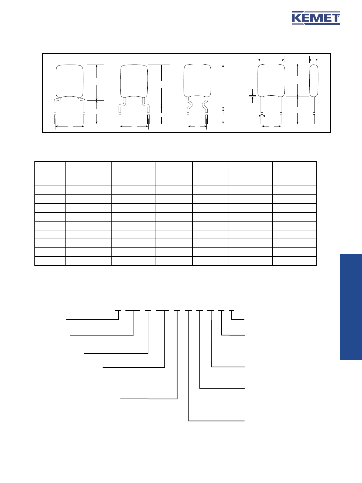
STANDARD LEAD CONFIGURATION — OUTLINE DRAWINGS
*.276 (7.00) MIN.
C317
C322
C330
H
*
S
Drawings are not to scale. See table below for dimensions.
See page 10 for optional lead configurations.
C323
S
C333
H
*
.060
(1.52)
H
MAX.
*
D
S
L
C315
C320
C330
C340
C350
S
H
*
DIMENSIONS — INCHES & MILLIMETERS
CASE L H T S(1) D
Case
SIZE MAX. MAX. MAX. ±.030 (.78)
Size
C315 .150 (3.81) .210 (5.33) .130 (3.30) .100 (2.54) .020 (.51)
C315 0.150 (3.81) 0.210 (5.33) 0.100 0.150 0.100 (2.54) 0.020 (.51)
C317 .150 (3.81) .230 (5.84) .130 (3.30) .200 (5.08) .020 (.51)
C317 0.150 (3.81) 0.230 (5.84) 0.100 0.150 0.200 (5.08) 0.020 (.51)
C320 .200 (5.08) .260 (6.60) .150 (3.81) .100 (2.54) .020 (.51)
C320 0.200 (5.08) 0.260 (6.60) 0.125 0.200 0.100 (2.54) 0.020 (.51)
C322 .200 (5.08) .260 (6.60) .150 (3.81) .200 (5.08) .020 (.51)
C322 0.200 (5.08) 0.260 (6.60) 0.125 0.200 0.200 (5.08) 0.020 (.51)
C323 .200 (5.08) .320 (8.13) .150 (3.81) .200 (5.08) .020 (.51)
C323 0.200 (5.08) 0.320 (8.13) 0.125 0.200 0.200 (5.08) 0.020 (.51)
C330 0.300 (7.62) 0.360 (9.14) 0.150 0.250 0.200 (5.08) 0.020 (.51)
C330 .300 (7.62) .360 (9.14) .200 (5.08) .200 (5.08) .020 (.51)
C333 0.300 (7.62) 0.390 (9.91) 0.150 0.250 0.200 (5.08) 0.020 (.51)
C333 .300 (7.62) .390 (9.91) .200 (5.08) .200 (5.08) .020 (.51)
C340 0.400 (10.16) 0.460 (11.68) 0.150 0.270 0.200 (5.08) 0.020 (.51)
C340 .400 (10.16) .460 (11.68) .200 (5.08) .200 (5.08) .020 (.51)
C350 0.500 (12.70) 0.560 (14.22) 0.200 0.270 0.400 (10.16) 0.025 (.64)
C350 .500 (12.70) .560 (14.22) .250 (6.35) .400 (10.16) .025 (.64)
NOTE: 1 inch = 25.4 mm.
NOTE: (1) Measured at seating plane.
L
Max.
H.
Max
Standard
T
Max.
High
Voltage
T Max.
S(1)
±.030 (.78)
D
+.004(.10)
+.004 (.10)- .001 (.025)
-.001(.025)
T
ORDERING INFORMATION
C
320
C
102
M
R
1
CERAMIC
CASE SIZE
(See Table Above)
SPECIFICATION
C — Standard
CAPACITANCE, CODE
Expressed in Picofarads (pF)
First Two Digits — Significant Figures
Third Digit — Number of Zeros (Use 9 for 1.0
thru 9.9 pF. Example: 2.2pF — 229)
CAP ACIT ANCE T OLERANCE
D — ±0.5 pF
F — ±1%
G — ±2%
J — ±5%
K — ±10%
M — ±20%
P — 0%, +100%
Z — -20, +80%
*Part Number Example: C320C102M1R5CA (14 digits – no spaces)
T
5
For packaging information, see pages 40, and 41.
© KEMET Electronics Corporation, P.O. Box 5928, Greenville, S.C. 29606, (864) 963-6300 9
*
A
FAILURE RATE
A — Not Applicable
TERMINATION MATERIAL
T — 100% Tin
H — SnPb
100% Sn
C —
(
Not recommended for new design)
INTERNAL
CONSTRUCTION
5 — Standard
DIELECTRIC
EIA Designation
G — C0G (NP0) — Ultra-Stable
R — X7R — Stable
U — Z5U — General Purpose
RA TED VOLTA GE
50
1000
F — 1500
G — 2000
Z — 2500
H — 3000
2 — 200
1 — 100
5 —
C — 500
D —
Page 4
CERAMIC CONFORMALLY COATED/RADIAL
“STANDARD & HIGH VOLTAGE GOLDEN MAX”
© KEMET Electronics Corporation, P.O. Box 5928, Greenville, S.C. 29606, (864) 963-630010
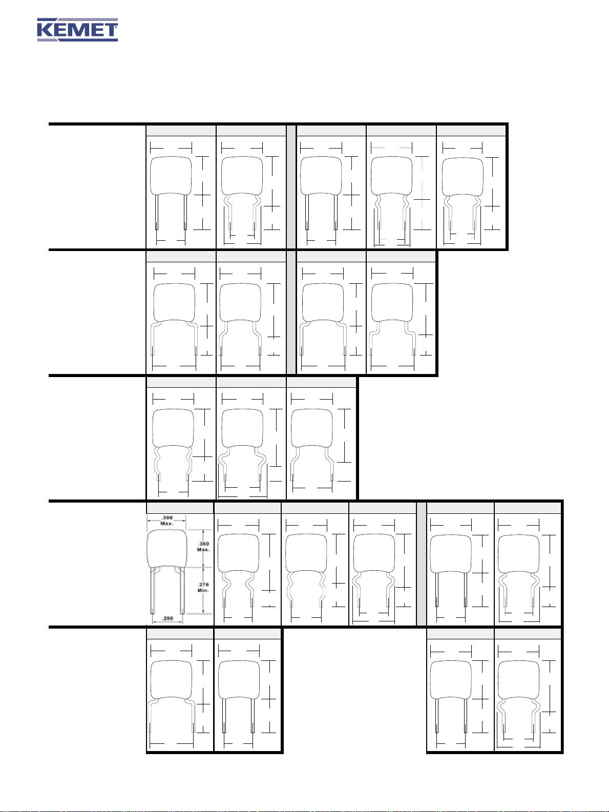
Note: Non-standard lead lengths are available in bulk only.
OPTIONAL CONFIGURATIONS BY LEAD SPACING
The preferred lead wire configurations are shown on page 9. However, additional configurations are
available. All available options, including those on page 9, are shown below grouped by lead spacing.
Lead Spacing
.100" ± .030
Lead Spacing
.200" ± .030
Lead Spacing
.200" ± .030
C 3 1 5
.150
MAX.
.100
C 3 1 7
.150
MAX.
.200
C 3 2 5
.200
MAX.
.210
MAX.
.276
MIN.
MAX.
.320
MAX.
.230
.276
MIN.
C 3 1 6
.150
MAX.
.100
.200
C 3 1 8
.150
MAX.
.200
C 3 2 7
.200
MAX.
.230
MAX.
.230
±.030
.235
MAX.
.276
MIN.
.350
MAX.
C 3 2 0
.200
MAX.
.260
MAX.
.276
MIN.
.100
C 3 2 2 C 3 2 3
.200
MAX.
.260
MAX.
.276
MIN.
.200
C 3 2 8
.200
MAX.
.325
MAX.
C 3 2 4 C 3 2 6
.200
MAX.
.100
.125
.200
MAX.
.200
.260
MAX.
.276
MIN.
.320
MAX.
.276
MIN.
.200
MAX.
.100
.200
.350
MAX.
.230
± .030
Lead Spacing
.200" ± .030
Note: C330 Shoulder
bend leads:
X7R/50V 683-105
Z5U/100V 683-334
Lead Spacing
.250" ± .030
(Available in
bulk only)
.200
C 3 3 0
.300
MAX.
.200
C 3 2 1
.200
MAX.
.250
.276
MIN.
.360
MAX.
.276
MIN.
.260
MAX.
.276
MIN.
.200
.270
C 3 3 3
.300
MAX.
.200
C 3 3 1
.300
MAX.
.250
.390
MAX.
.276
MIN.
.360
MAX.
.276
MIN.
.230
±.030
.276
MIN.
.200
C 3 3 5
.300
MAX.
.420
MAX.
.276
MIN.
.200
Lead Spacing
.400" ± .030
(Available in
C 3 3 6
.300
MAX.
.450
MAX.
.230
±.030
.200
.300
bulk only)
C 3 4 0
.400
MAX.
.200
C 3 5 0
.500
MAX.
.400
.460
MAX.
.276
MIN.
.560
MAX.
.276
MIN.
C 3 4 6
.400
MAX.
.200
.320
C 3 5 6
.500
MAX.
.400
.520
.590
MAX.
.230
±.030
.670
MAX.
.230
±.030
Page 5
© KEMET Electronics Corporation, P.O. Box 5928, Greenville, S.C. 29606, (864) 963-6300 11
CERAMIC CONFORMALLY COATED/RADIAL
“STANDARD & HIGH VOLTAGE GOLDEN MAX”
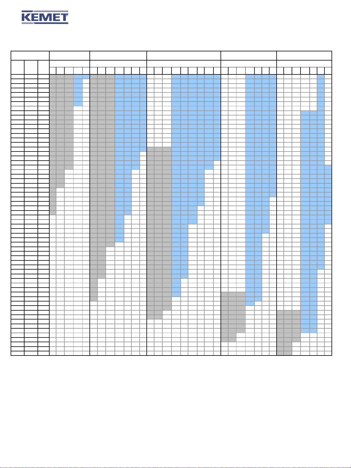
Golden Max
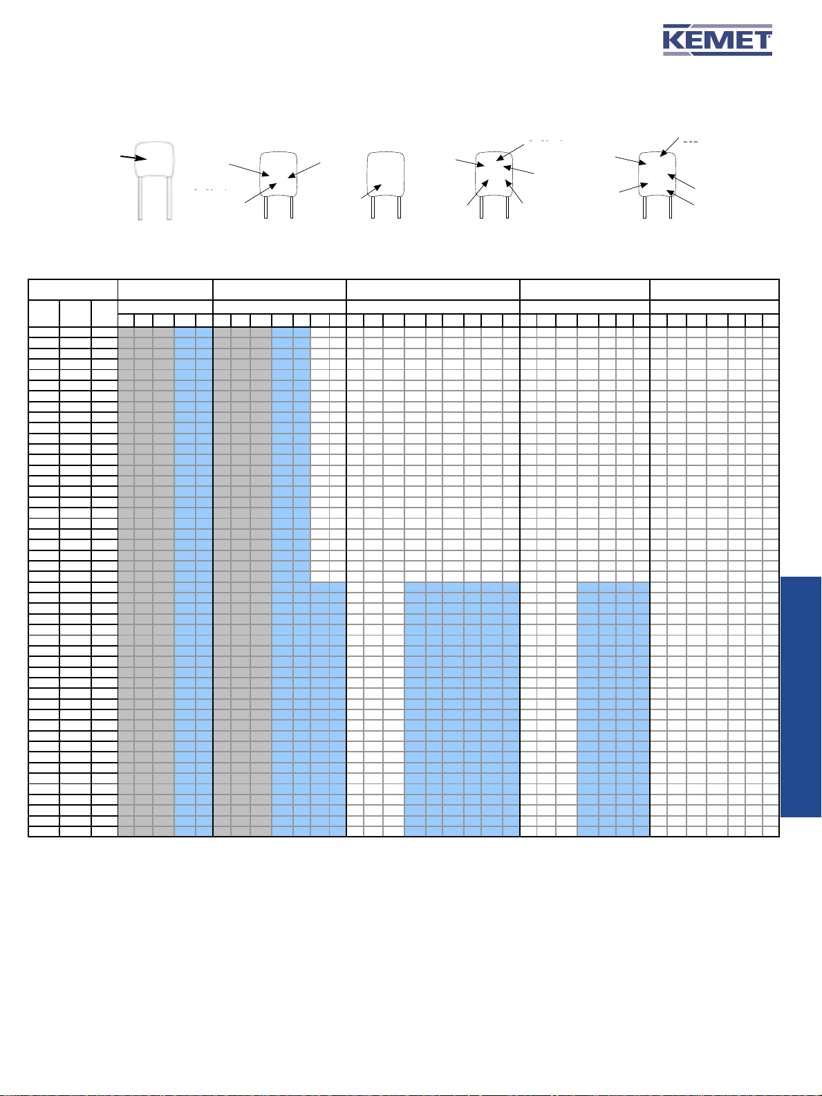
CAPACITOR MARKINGS
RATINGS & PART NUMBER REFERENCE: ULTRA-STABLE TEMPERATURE CHARACTERISTICS – C0G/NPO
For packaging information, see pages 40 and 41.
K
Manufacturer
(KEMET)
Style
Cap
Cap
1.0pF 109 D
1.1 119 D
1.2 129 D
1.3 139 D
1.5 159 D
1.6 169 D
1.8 189 D
2.0 209 D
2.2 229 D
2.4 249 D
2.7 279 D
3.0 309 D
3.3 339 D
3.6 369 D
3.9 399 D
4.3 439 D
4.7 479 D
5.1 519 D
5.6 569 D
6.2 629 D
6.8 689 D
7.5 759 D
8.2 829 D
9.1 919 D
10 100 J,K
11 110 J,K
12 120 J,K
13 130 J,K
15 150 J,K
16 160 J,K
18 180 J,K
20 200 J,K
22 220 J,K
24 240 G,J,K
27 270 G,J,K
30 300 G,J,K
33 330 G,J,K
36 360 G,J,K
39 390 G,J,K
43 430 G,J,K
47 470 G,J,K
51 510 G,J,K
56 560 F,G,J
62 620 F,G,J
68 680 F,G,J
75 750 F,G,J
82 820 F,G,J
91 910 F,G,J
Cap
Code
Rated Voltage
5 - 50 volts
1 - 100 volts
2 - 200 volts
Dielectric
G - C0G
R - X7R
U - Z5U
Capacitance
Tolerance
Manufacturer
(KEMET)
Rated Voltage
5 - 50 volts
1 - 100 volts
2 - 200 volts
Capacitance
Tolerance
Front
K1K
Capacitance
Code
C31X & C32X Size
Back
102
Manufacturer
(KEMET)
Capacitance
Code
K5U
104M
C33X Size
C33X
Tol
50 100 200 500 1k 50 100 200 500 1k 1.5k 2k 50 100 200 500 1k 1.5k 2k 2.5k 3k 50 100 200 500 1k 2k 3k 50 100 200 500 1k 2k 3k
Manufacturer
C34X
(KEMET)
Rated
Voltage
C340 & C350 Size
KX7R
105K
100V
212
0
Dielectric
C0G
X7R
Z5U
Capacitance
& Tolerance
Date Code
C35XC31X C32X
WVDCWVDC WVDC WVDC WVDC
Page 6
© KEMET Electronics Corporation, P.O. Box 5928, Greenville, S.C. 29606, (864) 963-630012
For packaging information, see pages 40 and 41.
CERAMIC CONFORMALLY COATED/RADIAL
“STANDARD & HIGH VOLTAGE GOLDEN MAX”
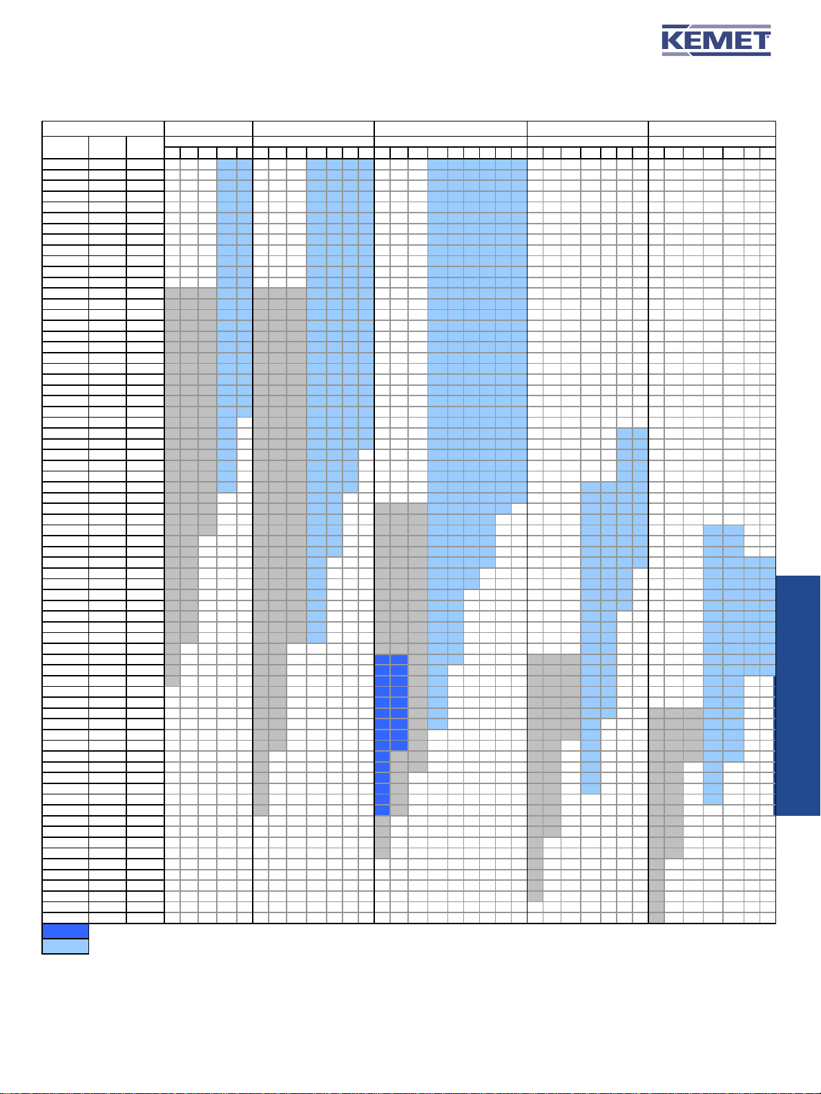
RATINGS & PART NUMBER REFERENCE: ULTRA-STABLE TEMPERATURE CHARACTERISTICS — C0G/NPO CONT.
Style
Cap
Code
Cap
Tol
Cap
100 101 F,G,J
110 111 F,G,J
120 121 F,G,J
130 131 F,G,J
150 151 F,G,J
160 161 F,G,J
180 181 F,G,J
200 201 F,G,J
220 221 F,G,J
240 241 F,G,J
270 271 F,G,J
300 301 F,G,J
330 331 F,G,J
360 361 F,G,J
390 391 F,G,J
430 431 F,G,J
470 471 F,G,J
510 511 F,G,J
560 561 F,G,J
620 621 F,G,J
680 681 F,G,J
750 751 F,G,J
820 821 F,G,J
910 911 F,G,J
1000 102 F,G,J
1100 112 F,G,J
1200 122 F,G,J
1300 132 F,G,J
1500 152 F,G,J
1600 162 F,G,J
1800 182 F,G,J
2000 202 F,G,J
2200 222 F,G,J
2400 242 F,G,J
2700 272 F,G,J
3000 302 F,G,J
3300 332 F,G,J
3600 362 F,G,J
3900 392 F,G,J
4300 432 F,G,J
4700 472 F,G,J
5100 512 F,G,J
5600 562 F,G,J
6200 622 F,G,J
6800 682 F,G,J
7500 752 F,G,J
8200 822 F,G,J
9100 912 F,G,J
.010uF 103 F,G,J
.015 123 F,G,J
.015 153 F,G,J
.018 183 F,G,J
.022 223 F,G,J
.027 273 F,G,J
.033 333 F,G,J
.039 393 F,G,J
.047 473 F,G,J
.056 563 F,G,J
.068 683 F,G,J
.082 823 F,G,J
.10 104 F,G,J
.12 124 F,G,J
C31X C32X C34X C35X
WVDC WVDC WVDC WVDC WVDC
50 100 200 500 1k 50 100 200 500 1k 1.5k 2k 50 100 200 500 1k 1.5k 2k 2.5k 3k 50 100 200 500 1k 2k 3k 50 100 200 500 1k 2k 3k
C33X
Page 7
For packaging information, see pages 40 and 41.
© KEMET Electronics Corporation, P.O. Box 5928, Greenville, S.C. 29606, (864) 963-6300 13
CERAMIC CONFORMALLY COATED/RADIAL
“STANDARD & HIGH VOLTAGE GOLDEN MAX”
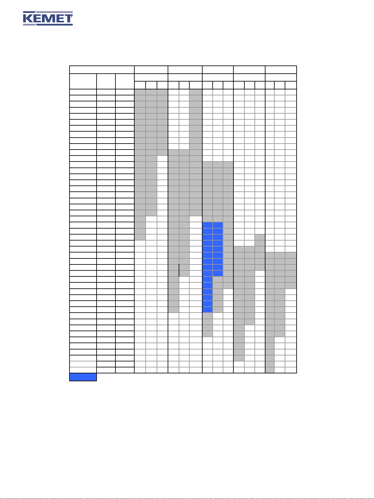
RATINGS & PART NUMBER REFERENCE: STABLE TEMPERATURE CHARACTERISTICS — X7R
Golden Max
Style
Cap
Code
Cap
50 100 200 500 1k 50 100 200 500 1k 1.5k 2k 50 100 200 500 1k 1.5k 2k 2.5k 3k 50 100 200 500 1k 2k 3k 50 100 200 500 1k 2k 3k
Tol
##
Cap
10pF 100 K,M,P,Z
12 120 K,M,P,Z
15 150 K,M,P,Z
18 180 K,M,P,Z
22 220 K,M,P,Z
27 270 K,M,P,Z
33 330 K,M,P,Z
39 390 K,M,P,Z
47 470 K,M,P,Z
56 560 K,M,P,Z
68 680 K,M,P,Z
82 820 K,M,P,Z
100 101 K,M,P,Z
120 121 K,M,P,Z
150 151 K,M,P,Z
180 181 K,M,P,Z
220 221 K,M,P,Z
270 271 K,M,P,Z
330 331 K,M,P,Z
390 391 K,M,P,Z
470 471 K,M,P,Z
560 561 K,M,P,Z
680 681 K,M,P,Z
820 821 K,M,P,Z
1000 102 K,M,P,Z
1200 122 K,M,P,Z
1500 152 K,M,P,Z
1800 182 K,M,P,Z
2200 222 K,M,P,Z
2700 272 K,M,P,Z
3300 332 K,M,P,Z
3900 392 K,M,P,Z
4700 472 K,M,P,Z
5600 562 K,M,P,Z
6800 682 K,M,P,Z
8200 822 K,M,P,Z
.010uF 103 K,M,P,Z
.012 123 K,M,P,Z
.015 153 K,M,P,Z
.018 183 K,M,P,Z
.022 223 K,M,P,Z
.027 273 K,M,P,Z
.033 333 K,M,P,Z
.039 393 K,M,P,Z
.047 473 K,M,P,Z
.056 563 K,M,P,Z
.068 683 K,M,P,Z
.082 823 K,M,P,Z
.10 104 K,M,P,Z
.12 124 K,M,P,Z
.15 154 K,M,P,Z
.18 184 K,M,P,Z
.22 224 K,M,P,Z
.27 274 K,M,P,Z
.33 334 K,M,P,Z
.39 394 K,M,P,Z
.47 474 K,M,P,Z
.56 564 K,M,P,Z
.68 684 K,M,P,Z
.82 824 K,M,P,Z
1.0 105 K,M,P,Z
1.2 125 K,M,P,Z
1.5 155 K,M,P,Z
1.8 185 K,M,P,Z
2.2 225 K,M,P,Z
2.7 275 K,M,P,Z
3.3 335 K,M,P,Z
3.9 395 K,M,P,Z
4.7 475 K,M,P,Z
5.6 565 K,M,P,Z
6.8 685 K,M,P,Z
C330 shoulder bend lead configuration is standard for these cap codes.
# X7R Dielectric--extended range value--Cap and DF measured @0.5Vrms.
C33X
C34X
C35XC31X C32X
WVDCWVDC WVDC WVDC WVDC
Page 8
© KEMET Electronics Corporation, P.O. Box 5928, Greenville, S.C. 29606, (864) 963-630014
CERAMIC CONFORMALLY COATED/RADIAL
“STANDARD & HIGH VOLTAGE GOLDEN MAX”
RATINGS & PART NUMBER REFERENCE
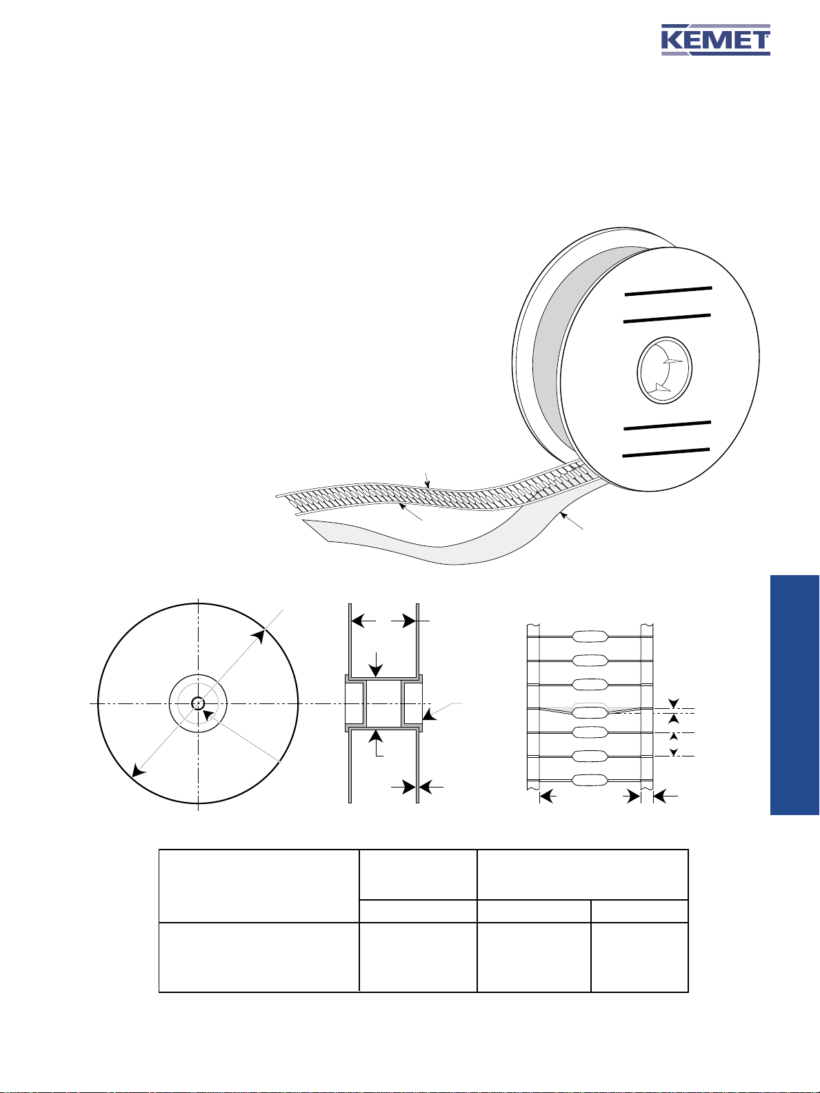
GENERAL PURPOSE TEMPERATURE CHARACTERISTIC – Z5U
For packaging information, see pages 40 and 41.
Cap
1000pF
1200
1500
1800
2200
2700
3300
3900
4700
5600
6800
8200
.010uF
.012
.015
.018
.022
.027
.033
.039
.047
.056
.068
.082
.10
.12
.15
.18
.22
.27
.33
.39
.47
.56
.68
.82
1.0
1.2
1.5
1.8
2.2
2.7
3.3
3.9
4.7
5.6
6.8
Style
Cap
102
122
152
182
222
272
332
392
472
562
682
822
103
123
153
183
223
273
333
393
473
563
683
823
104
124
154
184
224
274
334
394
474
564
684
824
105
125
155
185
225
275
335
395
475
565
685
Cap
Tol
M,P,Z
M,P,Z
M,P,Z
M,P,Z
M,P,Z
M,P,Z
M,P,Z
M,P,Z
M,P,Z
M,P,Z
M,P,Z
M,P,Z
M,P,Z
M,P,Z
M,P,Z
M,P,Z
M,P,Z
M,P,Z
M,P,Z
M,P,Z
M,P,Z
M,P,Z
M,P,Z
M,P,Z
M,P,Z
M,P,Z
M,P,Z
M,P,Z
M,P,Z
M,P,Z
M,P,Z
M,P,Z
M,P,Z
M,P,Z
M,P,Z
M,P,Z
M,P,Z
M,P,Z
M,P,Z
M,P,Z
M,P,Z
M,P,Z
M,P,Z
M,P,Z
M,P,Z
M,P,Z
M,P,Z
Code
C330 shoulder bend lead configuration is standard for these cap codes.
C31X C32X
C33X
C34X
C35X
WWDCWWDC WWDC WWDC WWDC
50 100 200 50 100 200 50 100 200 50 100 200 50 100 200
Page 9
© KEMET Electronics Corporation, P.O. Box 5928, Greenville, S.C. 29606, (864) 963-6300 39
CERAMIC LEADED
PACKAGING INFORMATION
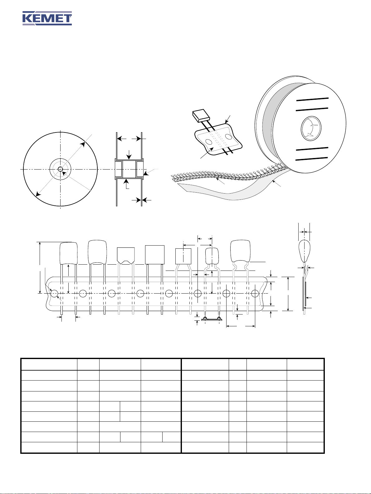
Tape and Reel Packaging
Ceramic Axial
Lead Tape and Reel Packaging
KEMET offers standard reeling of Molded and Conformally
Coated Axial Leaded Ceramic Capacitors for automatic insertion
or lead forming machines per EIA specification RS-296. KEMET’S
internal specification four-digit suffix, 7200, is placed at the end of
the part number to designate tape and reel packaging, ie:
C410C104Z5U5CA7200.
Paper (50 lb.) test minimum is inserted between the layers of
capacitors wound on reels for component pitch ≤ 0.400".
Capacitor lead length may extend only a maximum of .0625"
(1.59mm) beyond the tapes' edges. Capacitors are centered in a
row between the two tapes and will deviate only ± 0.031
(0.79mm) from the row center. A minimum of 36" (91.5 cm) leader
tape is provided at each end of the reel capacitors. Universal
splicing clips are used to connect the tape. Standard reel
quantities are shown on page 41.
Adhesive Tape
Figure 1
®
KEMET
®
KEMET
Table 1
Figure 2
10.5" - 14"
(26.67 -
35.56cm)
.655" ±0.010"
(16.6 ±0.25)
Dimensions in Inches & (Millimeters)
Component
Body Diameter
Adhesive Tape
.059" to .315"
*
31/4"
(82.6)
Component
Pitch "A"
0.020" or (±0.5mm) I III*
Greater Than
Component
Length
Hub
1
/8"
(3.18)
Inside Tape Spacing "B"
± 1.5mm (0.059")
Kraft Paper
Interleaving
Figure 3
See Table 1
(B)
.047" Max
(1.20)
See Table 1 (A)
*
.250" Nom.
(6.35)
0" (0mm) to 0.197" (5mm)
0.197" (5.01mm) to 0.394: (10mm)
* Not Available for Conformally Coated Parts.
0.197" or (5mm)
0.394" or (10mm)
2.062" (52.4mm)
2.874" (73mm)
Page 10
CERAMIC LEADED
PACKAGING INFORMATION
© KEMET Electronics Corporation, P.O. Box 5928, Greenville, S.C. 29606, (864) 963-630040
Ceramic Radial
Lead Tape and Reel Packaging
KEMET offers standard reeling of Molded and Conformally
Coated Radial Leaded Ceramic Capacitors for automatic
insertion per EIA specification RS-468. Parts are taped to a
tagboard carrier strip, and wound on a reel as shown in
Figure 1. Kraft paper interleaving is inserted between the
layers of capacitors on the reel. Ammopack is also available,
with the same lead tape configuration and package quantities.
Figure 1
Carrier Strip
®
KEMET
12"
(30.48 cm
.655" ±0.010"
0.25)
(16.6 ±
)
*
(82.6)
31/4"
.059" to .315"
Greater Than
Over All
Height
of T aped
Component
Hub
1
/8"
(3.18)
s
Figure 3: Standard Reel
H1
C315*
C320*
D
0
C340**
C6xx#
C056**
C066**
H
F
C330**
CK06**
CKR06**
C062**
Figure 2: Lead Tape Configuration (See Table Below)
Ceramic Radial Tape and Reel Dimensions in Millimeters & (Inches)
Dimension Symbol
Sprocket Hole Diameter
Sprocket Hole Pitch
Component Pitch
Lead Spacing (1)
Sprocket Hole Center
to Lead Center (1)
Sprocket Hole Center
to Component Center
Height to Seating Plane
(straight leads) (2)
Component Height
Above T ape Center
(1) Measured at the egress from the carrier tape, on the component side.
(2) Determined by a 4 digit suffix placed at the end of the part number, as follows:
7301 =
7303 =
Recommended for parts with formed leads.
Recommended for parts with straight leads.
Do
P0
P
F
P1
P2
H
H1
Nominal
mm (inch)
4.0 (.157)
12.7 (.500)
12.7 (.500)
5.08 2.54
(.20) (.10)
3.81 5.08
(.150) (.200)
6.35 (.250)
7301 7303
16.0 (.630) 18.0 (.709)
32.2 (1.27)
Tolerance
mm (inch) Dimension Symbol
± 0.2 (.008)
± 0.3 (.012)
± 0.3 (.012)
+0.6 -0.2
(+.024 -.008)
± 0.7 (.028)
± 1.3 (.051)
7301 7303
±0.5 (.020) Minimum
Maximum
Example: C322C104K5R5CA7301
Example: C320C104K5R5CA7303
Adhesive T
CK05**
CKR05**
C052**
P
P1
T
Height to Seating
Plane (formed leads) (2)
Component Alignment
Lead Protrusion
Composite T ape
Thickness
Overall T ape and
Lead Thickness
Carrier T ape Width
Hold-Down T ape
Width
Hold-Down T ape
Location
ape
C317**
C322**
C323**
P
2
H
Carrier Tape
0
C6xx#
C333**
L
1
P
0
H
7301 7303
0
16.0 (.630) 18.0 (.709)
∆h
L1
t
T
W
W0
W2
KEMET
Kraft Paper
Interleaving
(Note: Non-standard lead lengths
available in bulk only.)
∆H
1MM Max.
(.039")
W
2
W
W
0
W
2
* Lead spacings are 2.54mm
(.10") center-to-center.
** Lead spacings are 5.08mm
(.20") center-to-center.
# See page 15 for exact lead
configuration for Series.
Nominal
mm (inch)
4.0 (.157)
1.0 (.039)
0.7 (.051)
1.5 (.059)
18.0 (.709)
5.0 (.197)
3.0 (.118)
7301 7303
±0.5 (.020) Minimum
(+.039 -.020)
Tape
Carrier
Tolerance
mm (inch)
±0.2 (.008)
Maximum
±0.2 (.008)
Maximum
+1.0 - 0.5
Minimum
Maximum
®
Page 11
CERAMIC PACKAGING
CERAMIC LEADED
PACKAGING INFORMATION
KEMET
Series
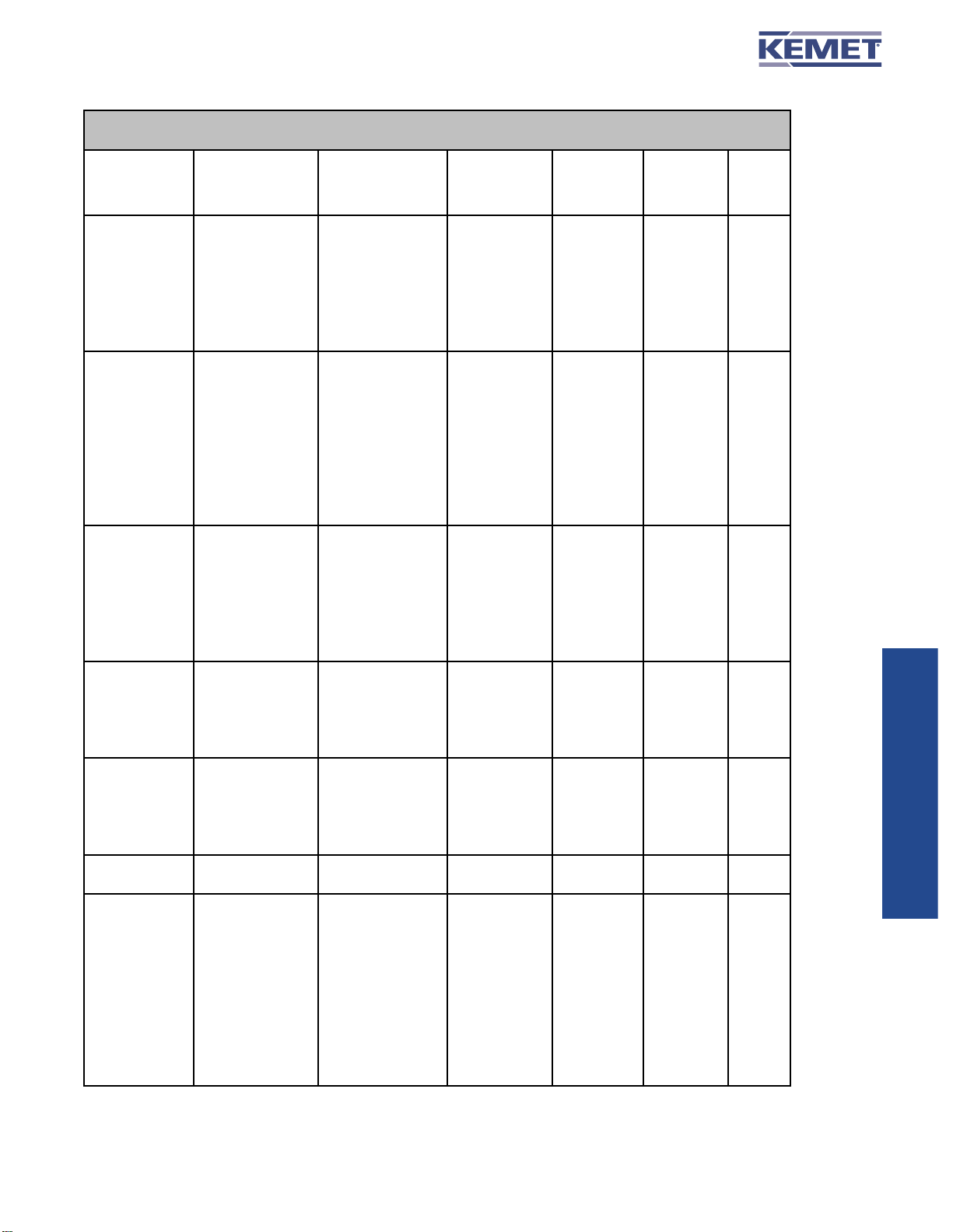
C114C-K-G CK12, CC75 MIL-C-11015/ 200/Box 5000 12"
C124C-K-G CK13, CC76 MIL-PRF-20 200/Box 5000 12"
C192C-K-G CK14, CC77 100/Box 3000 12"
C202C-K CK15 25/Box 500 12"
C222C-K CK16 10/Tray 300 12"
C052C-K-G CK05, CC05 100/Bag 2000 2000 12"
C062C-K-G CK06, CC06 100/Bag 1500 1500 12"
C114G CCR75 MIL-PRF-20 200/Box 5000 12"
C124G CCR76 200/Box 5000 12"
C192G CCR77 100/Box 3000 12"
C202G CC78-CCR78 25/Box 500 12"
C222G CC79-CCR79 10/Tray 300 12"
C052/56G CCR05 100/Bag 1700 12"
C062/66G CCR06 100/Bag 1500 12"
C512G CC07-CCR07 Footnote (2) N/A N/A
C522G CC08-CCR08 Footnote (2) N/A N/A
C114T CKR11 MIL-PRF-39014 200/Box 5000 12"
C124T CKR12 200/Box 5000 12"
C192T CKR14 100/Box 3000 12"
C202T CKR15 25/Box 500 12"
C222T CKR16 10/Tray 300 12"
C052/56T CKR05 100/Bag 1700 12"
C062/66T CKR06 100/Bag 1500 12"
C31X 500/Bag 2500 2500 12"
C32X 500/Bag 2500 2500 12"
C33X 250/Bag 1500 1500 12"
C340 100/Bag 1000 1000 12"
C350 50/Bag N/A N/A N/A
C410 300/Box 4000 5000 12"
C412 200/Box 4000 5000 12"
C420 300/Box 4000 5000 12"
C430 200/Box 2000 2500 12"
C440 200/Box 2000 2500
C512 N/A N/A Footnote (2) N/A
C522 N/A N/A Footnote (2) N/A
C617 500/Bag
C622/C623 500/Bag
C627/C628 500/Bag
C630/C631 250/Bag
C637/C638 250/Bag
C640/C641 100/Bag
C642/C643 100/Bag
C647/C648 100/Bag
C657/C658 50/Bag
C667/C668 50/Bag
NOTE: (1) Standard packaging refers to number of pieces per bag, tray or vial.
(2) Quantity varies. For further details, please consult the factory.
Military
Style
Military
Specification
Standard (1)
Bulk
Quantity
Ammo Pack
Quantity
Maximum
Maximum
Reel
Quantity
Reel
Size
12"
N/A
N/A
Tape and Reel Packaging
© KEMET Electronics Corporation, P.O. Box 5928, Greenville, S.C. 29606, (864) 963-6300 41
 Loading...