

l
s
f
查询MMSZ18ET1G供应商
MMSZ2V4ET1 Series
Zener Voltage Regulators
500 mW SOD−123 Surface Mount
Three complete series of Zener diodes are offered in the convenient,
surface mount plastic SOD−123 package. These devices provide a
convenient alternative to the leadless 34−package style.
Specification Features
• 500 mW Rating on FR−4 or FR−5 Board
• Wide Zener Reverse Voltage Range − 2.4 V to 56 V
• Package Designed for Optimal Automated Board Assembly
• Small Package Size for High Density Applications
• ESD Rating of Class 3 (>16 kV) per Human Body Model
• Peak Power − 225 W (8 X 20 ms)
• Pb−Free Packages are Available
Mechanical Characteristics
CASE: Void-free, transfer-molded, thermosetting plastic case
FINISH: Corrosion resistant finish, easily solderable
MAXIMUM CASE TEMPERATURE FOR SOLDERING PURPOSES:
260°C for 10 Seconds
POLARITY: Cathode indicated by polarity band
FLAMMABILITY RATING: UL 94 V−0
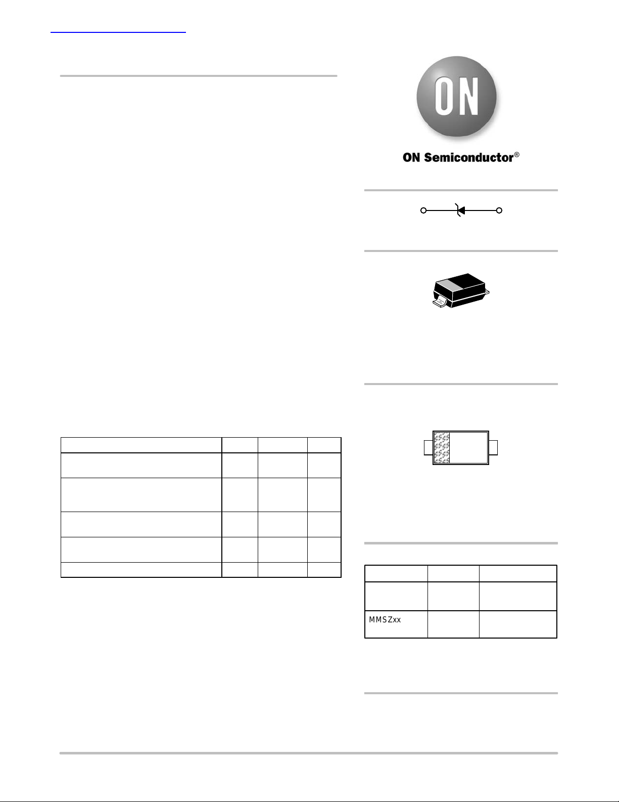
http://onsemi.com
1
Cathode
1
SOD−123
CASE 425
STYLE 1
MARKING DIAGRAM
2
Anode
2
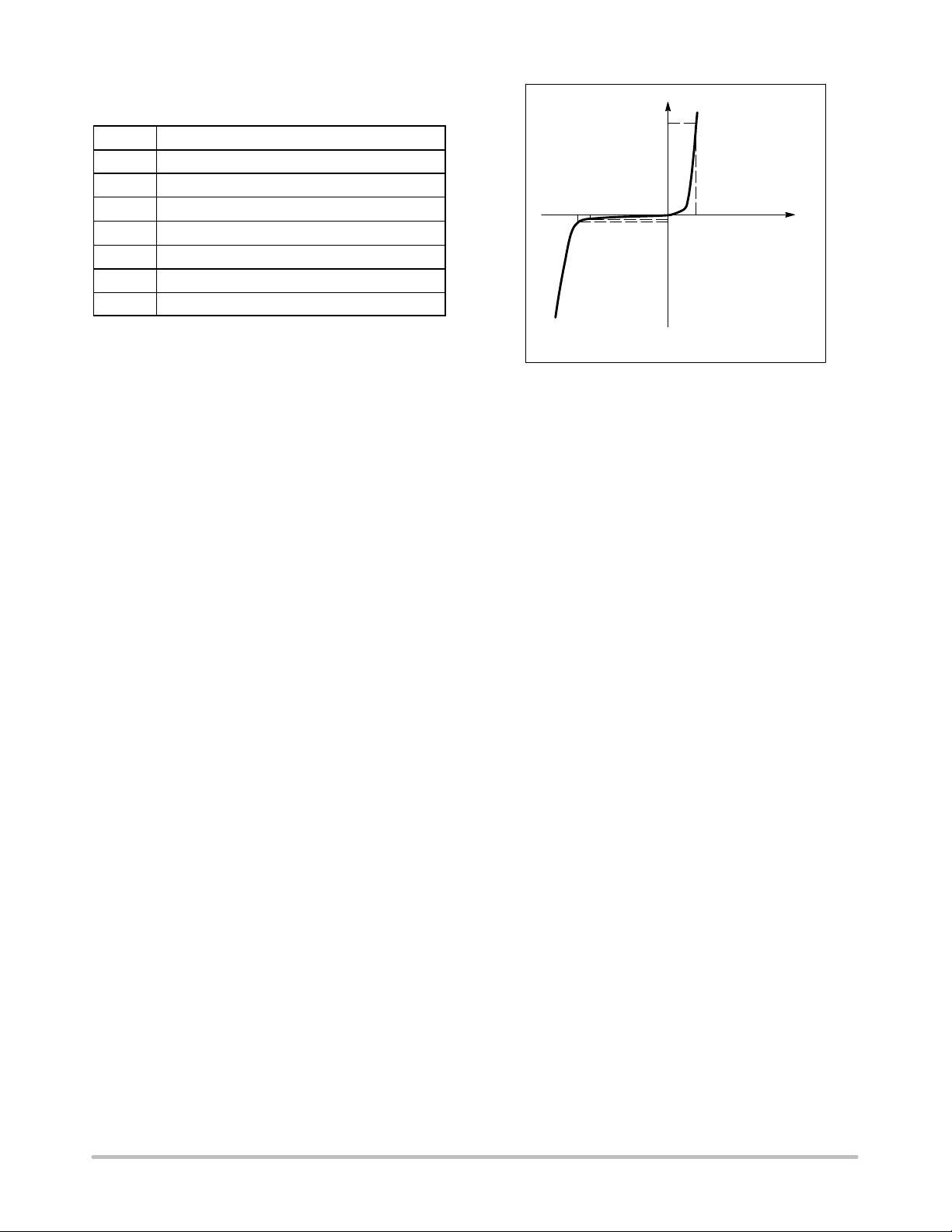
MAXIMUM RATINGS
Rating Symbol Max Unit
Peak Power Dissipation @ 20 ms (Note 1)
@ TL ≤ 25°C
Total Power Dissipation on FR−5 Board,
(Note 2) @ TL = 75°C
Derated above 75°C
Thermal Resistance, Junction−to−Ambient
(Note 3)
Thermal Resistance, Junction−to−Lead
(Note 3)
Junction and Storage Temperature Range TJ, T
Maximum ratings are those values beyond which device damage can occur.
Maximum ratings applied to the device are individual stress limit values (not
normal operating conditions) and are not valid simultaneously. If these limits are
exceeded, device functional operation is not implied, damage may occur and
reliability may be affected.
1. Nonrepetitive current pulse per Figure 11
2. FR−5 = 3.5 X 1.5 inches, using the ON minimum recommended footprint
3. Thermal Resistance measurement obtained via infrared Scan Method
P
pk
P
D
R
q
JA
R
q
JL
stg
225 W
500
6.7
340 °C/W
150 °C/W
−55 to +150 °C
mW
mW/°C
xxx M G
G
xxx = Device Code
M = Date Code
G = Pb−Free Package
(Note: Microdot may be in either location)
ORDERING INFORMATION
Device Package Shipping
MMSZxxxET1 SOD−123
(Pb−Free)
MMSZxxxET3 SOD−123
(Pb−Free)
†For information on tape and reel specifications,
including part orientation and tape sizes, please
refer to our Tape and Reel Packaging Specification
Brochure, BRD8011/D.
3000/Tape & Reel
10,000/Tape & Ree
†
DEVICE MARKING INFORMATION
See specific marking information in the device marking
column of the Electrical Characteristics table on page 3 o
this data sheet.
© Semiconductor Components Industries, LLC, 2006
January, 2006 − Rev. 5
1 Publication Order Number:
MMSZ2V4ET1/D
MMSZ2V4ET1 Series
ELECTRICAL CHARACTERISTICS (T
= 25°C unless
A
otherwise noted, VF = 0.95 V Max. @ IF = 10 mA)
Symbol Parameter
V
I
Z
V
V
Reverse Zener Voltage @ I
Z
Reverse Current
ZT
Maximum Zener Impedance @ I
ZT
I
Reverse Leakage Current @ V
R
Reverse Voltage
R
I
Forward Current
F
Forward Voltage @ I
F
ZT
ZT
R
F
I
I
F
VRV
Z
I
V
R
F
I
ZT
Zener Voltage Regulator
V
http://onsemi.com
2

MMSZ2V4ET1 Series
ELECTRICAL CHARACTERISTICS (T
Device
Device
Marking
= 25°C unless otherwise noted, VF = 0.9 V Max. @ IF = 10 mA)
A
VZ1 (V)
(Notes 4 and 5)
@ I
= 5 mA @ I
ZT1
Min Nom Max
Z
ZT1
(Note 6)
W
VZ2 (V)
(Notes 4 and 5)
Min Max
Z
ZT2
(Note 6)
= 1 mA IR @ V
ZT2
Max Reverse
Leakage Current
W mA
R
V
MMSZ2V4ET1, G CL1 2.28 2.4 2.52 100 1.7 2.1 600 50 1
MMSZ2V7ET1, G CL2 2.57 2.7 2.84 100 1.9 2.4 600 20 1
MMSZ3V0ET1 CL3 2.85 3.0 3.15 95 2.1 2.7 600 10 1
MMSZ3V3ET1, G CL4 3.14 3.3 3.47 95 2.3 2.9 600 5 1
MMSZ3V6ET1, G CL5 3.42 3.6 3.78 90 2.7 3.3 600 5 1
MMSZ3V9ET1, G CL6 3.71 3.9 4.10 90 2.9 3.5 600 3 1
MMSZ4V3ET1 CL7 4.09 4.3 4.52 90 3.3 4.0 600 3 1
MMSZ4V7ET1 CL8 4.47 4.7 4.94 80 3.7 4.7 500 3 2
MMSZ5V1ET1, G CL9 4.85 5.1 5.36 60 4.2 5.3 480 2 2
MMSZ5V6ET1 CM1 5.32 5.6 5.88 40 4.8 6.0 400 1 2
MMSZ6V2ET1 CM2 5.89 6.2 6.51 10 5.6 6.6 150 3 4
MMSZ6V8ET1 CM3 6.46 6.8 7.14 15 6.3 7.2 80 2 4
MMSZ7V5ET1 CM4 7.13 7.5 7.88 15 6.9 7.9 80 1 5
MMSZ8V2ET1 CM5 7.79 8.2 8.61 15 7.6 8.7 80 0.7 5
MMSZ9V1ET1 CM6 8.65 9.1 9.56 15 8.4 9.6 100 0.5 6
MMSZ10ET1, G CM7 9.50 10 10.50 20 9.3 10.6 150 0.2 7
MMSZ11ET1 CM8 10.45 11 11.55 20 10.2 11.6 150 0.1 8
MMSZ12ET1, G CM9 11.40 12 12.60 25 11.2 12.7 150 0.1 8
MMSZ13ET1 CN1 12.35 13 13.65 30 12.3 14.0 170 0.1 8
MMSZ15ET1, G CN2 14.25 15 15.75 30 13.7 15.5 200 0.05 10.5
MMSZ16ET1, G CN3 15.20 16 16.80 40 15.2 17.0 200 0.05 11.2
MMSZ18ET1, G CN4 17.10 18 18.90 45 16.7 19.0 225 0.05 12.6
MMSZ20ET1, G CN5 19.00 20 21.00 55 18.7 21.1 225 0.05 14
MMSZ22ET1, G CN6 20.90 22 23.10 55 20.7 23.2 250 0.05 15.4
MMSZ24ET1 CN7 22.80 24 25.20 70 22.7 25.5 250 0.05 16.8
4. The type numbers shown have a standard tolerance of ±5% on the nominal Zener Voltage.
5. Tolerance and Voltage Designation: Zener Voltage (VZ) is measured with the Zener Current applied for PW = 1 ms.
6. ZZT and ZZK are measured by dividing the AC voltage drop across the device by the AC current applied. The specified limits are for
I
Z(AC)
= 0.1 I
with the AC frequency = 1 kHz.
Z(DC),
Devices listed in bold, italic are ON Semiconductor Preferred devices. Preferred devices are recommended choices for future use and
best overall value.
*The “G” suffix indicates Pb−Free package available.
http://onsemi.com
3

MMSZ2V4ET1 Series
ELECTRICAL CHARACTERISTICS (T
Device
Device
Marking
= 25°C unless otherwise noted, VF = 0.9 V Max. @ IF = 10 mA)
A
VZ1 (V)
(Notes 7 and 8)
@ I
= 2 mA @ I
ZT1
Min Nom Max
Z
ZT1
(Note 9)
W
VZ2 (V)
(Notes 7 and 8)
= 0.1 mA
ZT2
Min Max
Z
ZT2
(Note 9)
@ I
=
ZT2
0.5 mA
W mA
Max Reverse
Leakage Current
IR @ V
R
V
MMSZ27ET1, G CN8 25.65 27 28.35 80 25 28.9 300 0.05 18.9
MMSZ30ET1 CN9 28.50 30 31.50 80 27.8 32 300 0.05 21
MMSZ33ET1 CP1 31.35 33 34.65 80 30.8 35 325 0.05 23.1
MMSZ36ET1 CP2 34.20 36 37.80 90 33.8 38 350 0.05 25.2
MMSZ39ET1 CP3 37.05 39 40.95 130 36.7 41 350 0.05 27.3
MMSZ43ET1, G CP4 40.85 43 45.15 150 39.7 46 375 0.05 30.1
MMSZ47ET1 CP5 44.65 47 49.35 170 43.7 50 375 0.05 32.9
MMSZ51ET1 CP6 48.45 51 53.55 180 47.6 54 400 0.05 35.7
MMSZ56ET1 CP7 53.20 56 58.80 200 51.5 60 425 0.05 39.2
7. The type numbers shown have a standard tolerance of ±5% on the nominal Zener Voltage.
8. Tolerance and Voltage Designation: Zener Voltage (VZ) is measured with the Zener Current applied for PW = 1 ms.
9. ZZT and ZZK are measured by dividing the AC voltage drop across the device by the AC current applied. The specified limits are for
I
Z(AC)
= 0.1 I
with the AC frequency = 1 kHz.
Z(DC),
Devices listed in bold, italic are ON Semiconductor Preferred devices. Preferred devices are recommended choices for future use and
best overall value.
*The “G” suffix indicates Pb−Free package available.
http://onsemi.com
4
MMSZ2V4ET1 Series
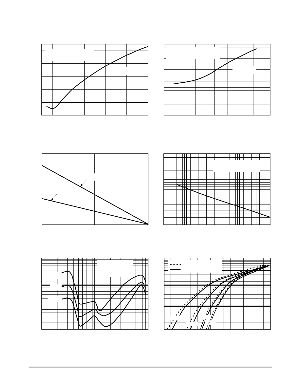
8
100
0
0
.2
TYPICAL CHARACTERISTICS
7
TYPICAL TC VALUES
6
FOR MMSZ2V4T1 SERIES
5
4
3
10
, TEMPERATURE COEFFICIENT (mV/ C)°θ
VZ
2
1
0
−1
−2
1
−3
VZ, NOMINAL ZENER VOLTAGE (V)
VZ @ I
ZT
12111098765432
Figure 1. Temperature Coefficients
(Temperature Range −55°C to +150°C)
1.2
1.0
0.8
0.6
PD versus T
PD versus T
A
L
1000
TYPICAL TC VALUES
FOR MMSZ2V4T1 SERIES
VZ @ I
ZT
, TEMPERATURE COEFFICIENT (mV/ C)°θ
VZ
10 10
VZ, NOMINAL ZENER VOLTAGE (V)
Figure 2. Temperature Coefficients
(Temperature Range −55°C to +150°C)
RECTANGULAR
WAVEFORM, TA = 25°C
100
0.4
, POWER DISSIPATION (WATTS)
D
0.2
P
1000
100
10
, DYNAMIC IMPEDANCE ( )Ω
ZT
Z
0
1
T, TEMPERATURE (°C)
Figure 3. Steady State Power Derating
TJ = 25°C
I
= 0.1 I
Z(AC)
IZ = 1 mA
5 mA
20 mA
VZ, NOMINAL ZENER VOLTAGE
f = 1 kHz
101
Z(DC)
1501251007550250
100
10
, PEAK SURGE POWER (WATTS)
pk
P
1
0.1
1 10 100 100
PW, PULSE WIDTH (ms)
Figure 4. Maximum Nonrepetitive Surge Power
1000
75 V (MMSZ5267BT1)
91 V (MMSZ5270BT1)
100
10
, FORWARD CURRENT (mA)
F
I
150°C
1
25°C
75°C
VF, FORWARD VOLTAGE (V)
0°C
1
1.11.00.90.80.70.60.50.4
Figure 5. Effect of Zener Voltage on
Zener Impedance
http://onsemi.com
5
Figure 6. Typical Forward Voltage

MMSZ2V4ET1 Series
1000
0
1000
TYPICAL CHARACTERISTICS
100
C, CAPACITANCE (pF)
100
10
1
10
1
0 V BIAS
1 V BIAS
BIAS AT
50% OF VZ NOM
101
VZ, NOMINAL ZENER VOLTAGE (V)
Figure 7. Typical Capacitance
TA = 25°C
TA = 25°C
100
100
10
0.1
, LEAKAGE CURRENT ( A)μ
0.01
R
I
0.001
0.0001
0.00001
100
10
1
+150°C
+25°C
−55°C
9
80706050403020100
VZ, NOMINAL ZENER VOLTAGE (V)
Figure 8. Typical Leakage Current
TA = 25°C
1
, ZENER CURRENT (mA)
Z
0.1
I
0.01
VZ, ZENER VOLTAGE (V)
Figure 9. Zener Voltage versus Zener Current
(V
Up to 12 V)
Z
100
t
r
90
80
70
60
50
40
30
20
% OF PEAK PULSE CURRENT
10
0
020406080
, ZENER CURRENT (mA)
Z
0.1
I
0.01
1086420
12
10 30 50 70 90
Figure 10. Zener Voltage versus Zener Current
t
P
PEAK VALUE I
PULSE WIDTH (tP) IS DEFINED
AS THAT POINT WHERE THE
PEAK CURRENT DECAY = 8 ms
HALF VALUE I
t, TIME (ms)
RSM
@ 8 ms
RSM
/2 @ 20 ms
Figure 11. 8 × 20 ms Pulse Waveform
VZ, ZENER VOLTAGE (V)
(12 V to 91 V)
http://onsemi.com
6
MMSZ2V4ET1 Series
PACKAGE DIMENSIONS
SOD−123
CASE 425−04
ISSUE E
D
1
H
E
2
E
b
A
A1
L
NOTES:
1. DIMENSIONING AND TOLERANCING PER ANSI
Y14.5M, 1982.
2. CONTROLLING DIMENSION: INCH.
MILLIMETERS INCHES
DIM MIN NOM MAX
A 0.94 1.17 1.35 0.037
A1 0.00 0.05 0.10 0.000
b 0.51 0.61 0.71 0.020
−−−
3.56H
2. ANODE
−−−
1.60
3.68 0.140
−−− −−−
c
E 2.54 2.69 2.84 0.100
E
L 0.25
STYLE 1:
PIN 1. CATHODE
MIN NOM MAX
0.15
0.055D 1.40 1.80
3.86
0.010
0.046
0.002
0.024
−−− −−−
0.063
0.106
0.145
−−− −−−
0.053
0.004
0.028
0.006
0.071
0.112
0.152
C
SOLDERING FOOTPRINT*
0.91
0.036
1.22
0.048
2.36
0.093
4.19
0.165
mm
ǒ
SCALE 10:1
inches
Ǔ
*For additional information on our Pb−Free strategy and soldering
details, please download the ON Semiconductor Soldering and
Mounting Techniques Reference Manual, SOLDERRM/D.
ON Semiconductor and are registered trademarks of Semiconductor Components Industries, LLC (SCILLC). SCILLC reserves the right to make changes without further notice
to any products herein. SCILLC makes no warranty, representation or guarantee regarding the suitability of its products for any particular purpose, nor does SCILLC assume any liability
arising out of the application or use of any product or circuit, and specifically disclaims any and all liability, including without limitation special, consequential or incidental damages.
“Typical” parameters which may be provided in SCILLC data sheets and/or specifications can and do vary in different applications and actual performance may vary over time. All
operating parameters, including “Typicals” must be validated for each customer application by customer’s technical experts. SCILLC does not convey any license under its patent rights
nor the rights of others. SCILLC products are not designed, intended, or authorized for use as components in systems intended for surgical implant into the body, or other applications
intended to support or sustain life, or for any other application in which the failure of the SCILLC product could create a situation where personal injury or death may occur. Should
Buyer purchase or use SCILLC products for any such unintended or unauthorized application, Buyer shall indemnify and hold SCILLC and its officers, employees, subsidiaries, affiliates,
and distributors harmless against all claims, costs, damages, and expenses, and reasonable attorney fees arising out of, directly or indirectly, any claim of personal injury or death
associated with such unintended or unauthorized use, even if such claim alleges that SCILLC was negligent regarding the design or manufacture of the part. SCILLC is an Equal
Opportunity/Affirmative Action Employer. This literature is subject to all applicable copyright laws and is not for resale in any manner.
PUBLICATION ORDERING INFORMATION
LITERATURE FULFILLMENT:
Literature Distribution Center for ON Semiconductor
P.O. Box 61312, Phoenix, Arizona 85082−1312 USA
Phone: 480−829−7710 or 800−344−3860 Toll Free USA/Canada
Fax: 480−829−7709 or 800−344−3867 Toll Free USA/Canada
Email: orderlit@onsemi.com
N. American Technical Support: 800−282−9855 Toll Free
USA/Canada
Japan: ON Semiconductor, Japan Customer Focus Center
2−9−1 Kamimeguro, Meguro−ku, Tokyo, Japan 153−0051
Phone: 81−3−5773−3850
http://onsemi.com
ON Semiconductor Website: http://onsemi.com
Order Literature: http://www.onsemi.com/litorder
For additional information, please contact your
local Sales Representative.
MMSZ2V4ET1/D
7
 Loading...