查询MMBZ10VAL供应商
MMBZ5V6ALT1 Series
Preferred Device
24 and 40 Watt Peak Power
Zener Transient Voltage
Suppressors
SOT−23 Dual Common Anode Zeners
for ESD Protection
http://onsemi.com
These dual monolithic silicon Zener diodes are designed for
applications requiring transient overvoltage protection capability. They
are intended for use in voltage and ESD sensitive equipment such as
computers, printers, business machines, communication systems,
medical equipment and other applications. Their d ual junction common
anode design protects two separate lines using only o ne p ackage. T hese
devices are ideal for situations where board space is at a premium.
Features
• Pb−Free Packages are Available
• SOT−23 Package Allows Either Two Separate Unidirectional
Configurations or a Single Bidirectional Configuration
• Working Peak Reverse Voltage Range − 3 V to 26 V
• Standard Zener Breakdown Voltage Range − 5.6 V to 33 V
• Peak Power − 24 or 40 Watts @ 1.0 ms (Unidirectional),
per Figure 5 Waveform
• ESD Rating of Class N (exceeding 16 kV) per the Human
Body Model
• Maximum Clamping Voltage @ Peak Pulse Current
• Low Leakage < 5.0 A
• Flammability Rating UL 94 V−O
Mechanical Characteristics
CASE:
Void-free, transfer-molded, thermosetting plastic case
FINISH: Corrosion resistant finish, easily solderable
MAXIMUM CASE TEMPERATURE FOR SOLDERING PURPOSES:
260°C for 10 Seconds
Package designed for optimal automated board assembly
Small package size for high density applications
Available in 8 mm Tape and Reel
1
2
3
SOT−23
1
2
See detailed ordering and shipping information in the package
dimensions section on page 2 of this data sheet.
DEVICE MARKING INFORMATION
See specific marking information in the device marking
column of the table on page 3 of this data sheet.
Preferred devices are recommended choices for future use
and best overall value.
CASE 318
STYLE 12
xxx = Device Code
M = Date Code
ORDERING INFORMATION
3
MARKING
DIAGRAM
xxx
M
Use the Device Number to order the 7 inch/3,000 unit reel.
Replace the “T1” with “T3” in the Device Number to order the
13 inch/10,000 unit reel.
Semiconductor Components Industries, LLC, 2004
August, 2004 − Rev. 7
1 Publication Order Number:
MMBZ5V6ALT1/D

MMBZ5V6ALT1 Series
MAXIMUM RATINGS
Rating Symbol Value Unit
Peak Power Dissipation @ 1.0 ms (Note 1) MMBZ5V6ALT1 thru MMBZ10VALT1
≤ 25°C MMBZ12VALT1 thru MMBZ33VALT1
@ T
L
Total Power Dissipation on FR−5 Board (Note 2) @ TA = 25°C
Derate above 25°C
Thermal Resistance Junction−to−Ambient R
Total Power Dissipation on Alumina Substrate (Note 3) @ TA = 25°C
Derate above 25°C
Thermal Resistance Junction−to−Ambient R
Junction and Storage Temperature Range TJ, T
Lead Solder Temperature − Maximum (10 Second Duration) T
Maximum ratings are those values beyond which device damage can occur. Maximum ratings applied to the device are individual stress limit
values (not normal operating conditions) and are not valid simultaneously . If these limits are exceeded, device functional operation is not implied,
damage may occur and reliability may be affected.
1. Non−repetitive current pulse per Figure 5 and derate above T
2. FR−5 = 1.0 x 0.75 x 0.62 in.
= 25°C per Figure 6.
A
3. Alumina = 0.4 x 0.3 x 0.024 in, 99.5% alumina.
*Other voltages may be available upon request.
ORDERING INFORMATION
Device Package Shipping
MMBZ5V6ALT1 SOT−23 3000 Tape & Reel
MMBZ5V6ALT1G SOT−23
MMBZ5V6ALT3 SOT−23 10,000 Tape & Reel
MMBZ5V6ALT3G SOT−23
MMBZ6VxALT1 SOT−23 3000 Tape & Reel
MMBZ6VxALT1G SOT−23
MMBZ6VxALT3 SOT−23 10,000 Tape & Reel
MMBZ6VxALT3G SOT−23
MMBZ9V1ALT1 SOT−23 3000 Tape & Reel
MMBZ9V1ALT1G SOT−23
MMBZ9V1ALT3 SOT−23 10,000 Tape & Reel
MMBZ9V1ALT13G SOT−23
MMBZxxVALT1 SOT−23 3000 Tape & Reel
MMBZxxVALT1G SOT−23
MMBZxxVALT3 SOT−23 10,000 Tape & Reel
MMBZxxVALT3G SOT−23
†For information on tape and reel specifications, including part orientation and tape sizes, please refer to our Tape and Reel Packaging
Specifications Brochure, BRD8011/D.
(Pb−Free)
(Pb−Free)
(Pb−Free)
(Pb−Free)
(Pb−Free)
(Pb−Free)
(Pb−Free)
(Pb−Free)
P
pk
24
40
°PD° 225
1.8
JA
556 °C/W
°PD° 300
2.4
JA
stg
L
417 °C/W
− 55 to +150 °C
260 °C
3000 Tape & Reel
10,000 Tape & Reel
3000 Tape & Reel
10,000 Tape & Reel
3000 Tape & Reel
10,000 Tape & Reel
3000 Tape & Reel
10,000 Tape & Reel
Watts
°mW°
mW/°C
°mW
mW/°C
†
http://onsemi.com
2

MMBZ5V6ALT1 Series
Device
I
@
Device
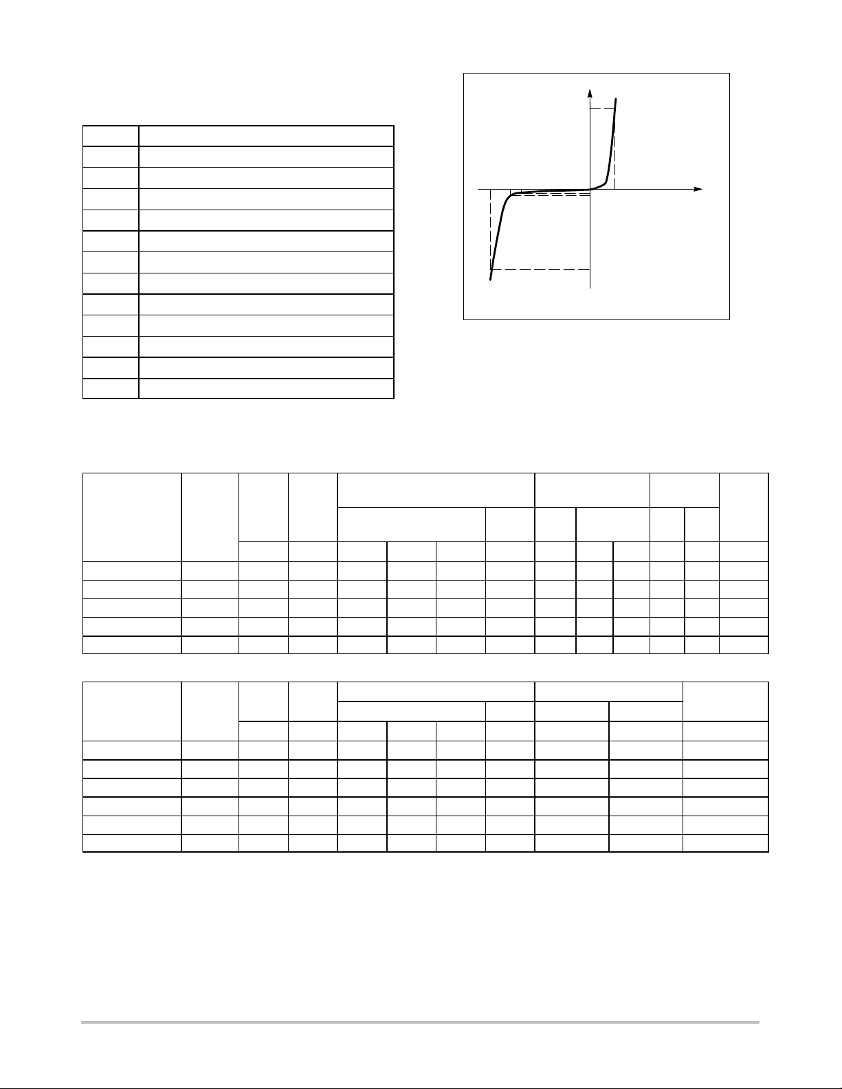
ELECTRICAL CHARACTERISTICS
(TA = 25°C unless otherwise noted)
UNIDIRECTIONAL (Circuit tied to Pins 1 and 3 or 2 and 3)
Symbol
V
V
I
PP
V
RWM
I
V
I
I
V
Z
I
ZK
Z
Maximum Reverse Peak Pulse Current
Clamping Voltage @ I
C
Working Peak Reverse Voltage
Maximum Reverse Leakage Current @ V
R
Breakdown Voltage @ I
BR
Test Current
T
Maximum Temperature Coefficient of V
BR
Forward Current
F
Forward Voltage @ I
F
Maximum Zener Impedance @ I
ZT
Reverse Current
Maximum Zener Impedance @ I
ZK
ELECTRICAL CHARACTERISTICS (T
Parameter
PP
T
F
RWM
BR
ZT
ZK
= 25°C unless otherwise noted)
A
VCV
V
RWM
BR
Uni−Directional TVS
I
I
F
I
V
R
F
I
T
I
PP
V
UNIDIRECTIONAL (Circuit tied to Pins 1 and 3 or Pins 2 and 3)
(VF = 0.9 V Max @ IF = 10 mA) 24 WATTS
Max Zener
Impedance (Note 5)
Z
ZT
@ I
T
ZT
ZZK @ I
Device
Marking
Breakdown Voltage
IR @
V
V
RWM
V
RWM
(Note 4) (V) @ I
BR
Volts A Min Nom Max mA mA V A
MMBZ5V6AL 5A6 3.0 5.0 5.32 5.6 5.88 20 11 1600 0.25 8.0 3.0 1.26
MMBZ6V2AL 6A2 3.0 0.5 5.89 6.2 6.51 1.0 − − − 8.7 2.76 2.80
MMBZ6V8AL 6A8 4.5 0.5 6.46 6.8 7.14 1.0 − − − 9.6 2.5 3.4
MMBZ9V1AL 9A1 6.0 0.3 8.65 9.1 9.56 1.0 − − − 14 1.7 7.5
MMBZ10VAL 10A 6.5 0.3 9.50 10 10.5 1.0 − − − 14.2 1.7 7.5
ZK
VC @ I
(Note 6)
V
CIPP
PP
V
BR
mV/C
(VF = 0.9 V Max @ IF = 10 mA) 40 WATTS
R
V
RWM
Device
Marking
V
RWM
Volts nA Min Nom Max mA V A
MMBZ12VAL 12A 8.5 200 11.40 12 12.60 1.0 17 2.35 7.5
MMBZ15VAL 15A 12 50 14.25 15 15.75 1.0 21 1.9 12.3
MMBZ18VAL 18A 14.5 50 17.10 18 18.90 1.0 25 1.6 15.3
MMBZ20VAL 20A 17 50 19.00 20 21.00 1.0 28 1.4 17.2
MMBZ27VAL 27A 22 50 25.65 27 28.35 1.0 40 1.0 24.3
MMBZ33VAL 33A 26 50 31.35 33 34.65 1.0 46 0.87 30.4
4. VBR measured at pulse test current IT at an ambient temperature of 25°C.
5. Z
and ZZK are measured by dividing the AC voltage drop across the device by the AC current applied. The specified limits are for I
ZT
= 0.1 I
6. Surge current waveform per Figure 5 and derate per Figure 6
, with the AC frequency = 1.0 kHz.
Z(DC)
Breakdown Voltage VC @ IPP (Note 6)
V
(Note 4) (V) @ I
BR
T
V
C
I
PP
http://onsemi.com
3
V
BR
mV/C
Z(AC)
 Loading...