

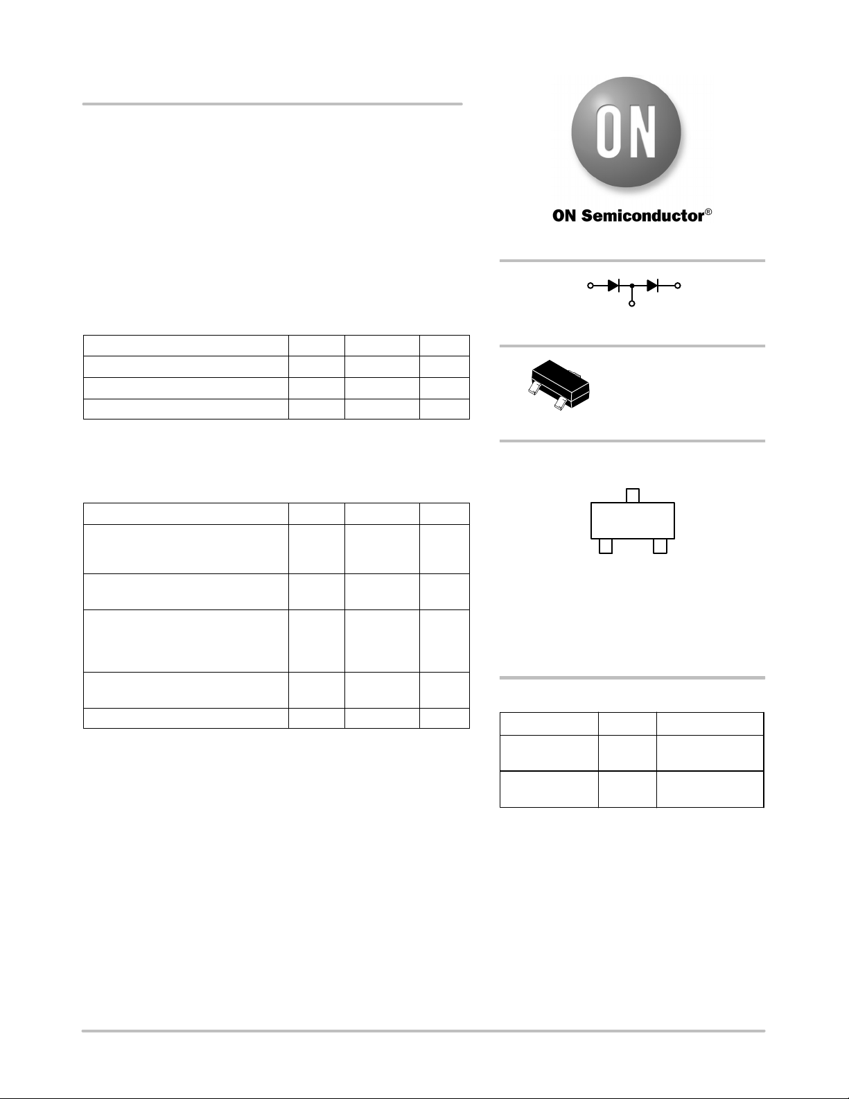
MMBD7000LT1G
Dual Switching Diode
Features
• These Devices are Pb−Free, Halogen Free/BFR Free and are RoHS
Compliant
http://onsemi.com
MAXIMUM RATINGS (EACH DIODE)
Rating Symbol Value Unit
Reverse Voltage V
Forward Current I
Peak Forward Surge Current I
Stresses exceeding Maximum Ratings may damage the device. Maximum
Ratings are stress ratings only. Functional operation above the Recommended
Operating Conditions is not implied. Extended exposure to stresses above the
Recommended Operating Conditions may affect device reliability.
R
F
FM(surge)
100 Vdc
200 mAdc
500 mAdc
THERMAL CHARACTERISTICS
Characteristic Symbol Max Unit
Total Device Dissipation FR−5 Board
(Note 1)TA = 25°C
Derate above 25°C
Thermal Resistance, Junction to
Ambient
Total Device Dissipation
Alumina Substrate, (Note 2)
TA = 25°C
Derate above 25°C
Thermal Resistance,
Junction−to−Ambient
Junction and Storage Temperature TJ, T
1. FR− 5 = 1.0 0.75 0.062 in.
2. Alumina = 0.4 0.3 0.024 in. 99.5% alumina.
P
D
R
q
JA
P
D
R
q
JA
stg
225
1.8
556 °C/W
300
2.4
417 °C/W
−55 to +150 °C
mW
mW/°C
mW
mW/°C
1
ANODE
1
2
3
CATHODE/ANODE
3
SOT−23 (TO−236AB)
2
CATHODE
CASE 318
STYLE 11
MARKING DIAGRAM
M5C MG
G
1
M5C = Specific Device Code
M = Date Code*
G = Pb−Free Package
(Note: Microdot may be in either location)
*Date Code orientation and/or overbar may
vary depending upon manufacturing location.
ORDERING INFORMATION
Device Package Shipping
MMBD7000LT1G SOT−23
(Pb−Free)
MMBD7000LT3G SOT−23
(Pb−Free)
3000 Tape & Reel
10,000 Tape & Reel
†
© Semiconductor Components Industries, LLC, 2009
August, 2009 − Rev. 5
†For information on tape and reel specifications,
including part orientation and tape sizes, please
refer to our Tape and Reel Packaging Specifications
Brochure, BRD8011/D.
1 Publication Order Number:
MMBD7000LT1/D
MMBD7000LT1G
ELECTRICAL CHARACTERISTICS (T
Characteristic
= 25°C unless otherwise noted) (EACH DIODE)
A
Symbol Min Max Unit
OFF CHARACTERISTICS
Reverse Breakdown Voltage
= 100 mAdc)
(I
(BR)
V
(BR)
100 − Vdc
Reverse Voltage Leakage Current
(VR = 50 Vdc)
(V
= 100 Vdc)
R
= 50 Vdc, 125°C)
(V
R
Forward Voltage
(IF = 1.0 mAdc)
(IF = 10 mAdc)
(IF = 100 mAdc)
Reverse Recovery Time
I
R
I
R2
I
R3
V
F
t
rr
−
−
−
0.55
0.67
0.75
1.0
3.0
100
0.7
0.82
1.1
− 4.0 ns
(IF = IR = 10 mAdc) (Figure 1)
Capacitance (VR = 0 V) C − 1.5 pF
mAdc
Vdc
+10 V
50 W OUTPUT
GENERATOR
820 W
PULSE
0.1 mF
2.0 k
100 mH
I
t
t
r
I
F
DUT
0.1 mF
p
10%
90%
t
50 W INPUT
SAMPLING
OSCILLOSCOPE
V
R
INPUT SIGNAL
F
I
R
Notes: 1. A 2.0 kW variable resistor adjusted for a Forward Current (IF) of 10 mA.
Notes: 2. Input pulse is adjusted so I
Notes: 3. tp » t
rr
is equal to 10 mA.
R(peak)
Figure 1. Recovery Time Equivalent Test Circuit
t
rr
i
R(REC)
t
= 1.0 mA
OUTPUT PULSE
(IF = IR = 10 mA; MEASURED
at i
= 1.0 mA)
R(REC)
http://onsemi.com
2

MMBD7000LT1G
CURVES APPLICABLE TO EACH DIODE
100
, FORWARD CURRENT (mA)
I
m
, REVERSE CURRENT ( A)
R
I
F
10
1.0
0.1
1.0
0.1
0.01
TA = 85°C
VF, FORWARD VOLTAGE (VOLTS)
TA = -40°C
TA = 25°C
1.0 1.20.2 0.4 0.6 0.8
Figure 2. Forward Voltage
10
TA = 150°C
TA = 125°C
TA = 85°C
TA = 55°C
0.001
0.68
0.64
0.60
0.56
, DIODE CAPACITANCE (pF)
D
C
0.52
TA = 25°C
0
10 20 30 40 50
VR, REVERSE VOLTAGE (VOLTS)
Figure 3. Leakage Current
0
2.0 4.0 6.0 8.0
VR, REVERSE VOLTAGE (VOLTS)
Figure 4. Capacitance
http://onsemi.com
3
MMBD7000LT1G
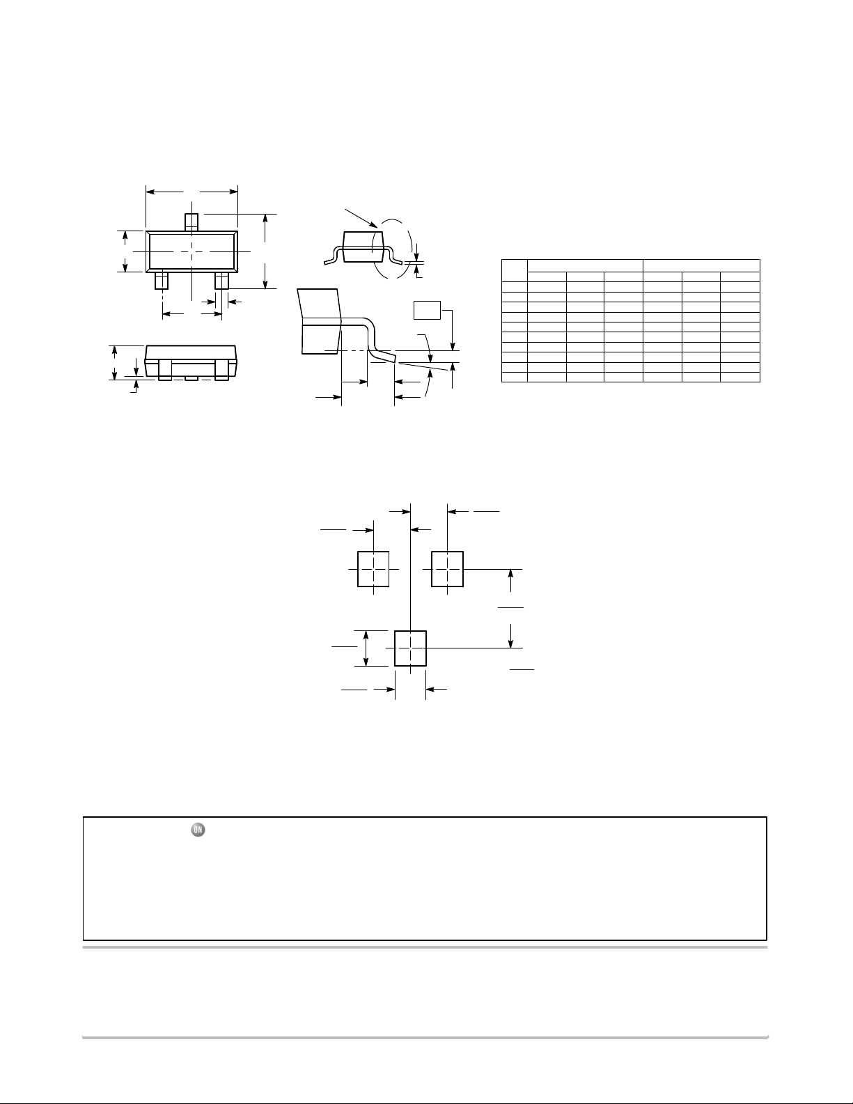
l
PACKAGE DIMENSIONS
SOT−23 (TO−236)
CASE 318−08
ISSUE AN
NOTES:
1. DIMENSIONING AND TOLERANCING PER ANSI
Y14.5M, 1982.
D
H
SEE VIEW C
E
c
0.25
3
E
12
b
e
q
A
L
A1
L1
VIEW C
2. CONTROLLING DIMENSION: INCH.
3. MAXIMUM LEAD THICKNESS INCLUDES LEAD
FINISH THICKNESS. MINIMUM LEAD
THICKNESS IS THE MINIMUM THICKNESS OF
BASE MATERIAL.
4. 318−01 THRU −07 AND −09 OBSOLETE, NEW
STANDARD 318−08.
DIMAMIN NOM MAX MIN
A1 0.01 0.06 0.10 0.001
b 0.37 0.44 0.50 0.015
c 0.09 0.13 0.18 0.003
D 2.80 2.90 3.04 0.110
E 1.20 1.30 1.40 0.047
e 1.78 1.90 2.04 0.070
L 0.10 0.20 0.30 0.004
L1
H
STYLE 11:
PIN 1. ANODE
MILLIMETERS
0.89 1.00 1.11 0.035
0.35 0.54 0.69 0.014 0.021 0.029
2.10 2.40 2.64 0.083 0.094 0.104
E
2. CATHODE
3. CATHODE−ANODE
INCHES
NOM MAX
0.040 0.044
0.002 0.004
0.018 0.020
0.005 0.007
0.114 0.120
0.051 0.055
0.075 0.081
0.008 0.012
SOLDERING FOOTPRINT
0.95
0.95
0.037
0.9
0.035
0.8
0.031
ON Semiconductor and are registered trademarks of Semiconductor Components Industries, LLC (SCILLC). SCILLC reserves the right to make changes without further notice
to any products herein. SCILLC makes no warranty, representation or guarantee regarding the suitability of its products for any particular purpose, nor does SCILLC assume any liability
arising out of the application or use of any product or circuit, and specifically disclaims any and all liability, including without limitation special, consequential or incidental damages.
“Typical” parameters which may be provided in SCILLC data sheets and/or specifications can and do vary in different applications and actual performance may vary over time. All
operating parameters, including “Typicals” must be validated for each customer application by customer’s technical experts. SCILLC does not convey any license under its patent rights
nor the rights of others. SCILLC products are not designed, intended, or authorized for use as components in systems intended for surgical implant into the body, or other applications
intended to support or sustain life, or for any other application in which the failure of the SCILLC product could create a situation where personal injury or death may occur. Should
Buyer purchase or use SCILLC products for any such unintended or unauthorized application, Buyer shall indemnify and hold SCILLC and its officers, employees, subsidiaries, affiliates,
and distributors harmless against all claims, costs, damages, and expenses, and reasonable attorney fees arising out of, directly or indirectly, any claim of personal injury or death
associated with such unintended or unauthorized use, even if such claim alleges that SCILLC was negligent regarding the design or manufacture of the part. SCILLC is an Equal
Opportunity/Affirmative Action Employer. This literature is subject to all applicable copyright laws and is not for resale in any manner.
0.037
SCALE 10:1
2.0
0.079
ǒ
inches
mm
Ǔ
PUBLICATION ORDERING INFORMATION
LITERATURE FULFILLMENT:
Literature Distribution Center for ON Semiconductor
P.O. Box 5163, Denver, Colorado 80217 USA
Phone: 303−675−2175 or 800−344−3860 Toll Free USA/Canada
Fax: 303−675−2176 or 800−344−3867 Toll Free USA/Canada
Email: orderlit@onsemi.com
N. American Technical Support: 800−282−9855 Toll Free
USA/Canada
Europe, Middle East and Africa Technical Support:
Phone: 421 33 790 2910
Japan Customer Focus Center
Phone: 81−3−5773−3850
http://onsemi.com
4
ON Semiconductor Website: www.onsemi.com
Order Literature: http://www.onsemi.com/orderlit
For additional information, please contact your loca
Sales Representative
MMBD7000LT1/D
 Loading...