

Page 1
查询MKP3V120供应商
MKP3V120, MKP3V240
Preferred Device
Sidac High V oltage
Bidirectional Triggers
Bidirectional devices designed for direct interface with the ac power
line. Upon reaching the breakover voltage in each direction, the device
switches from a blocking state to a low voltage on–state. Conduction
will continue like a Triac until the main terminal current drops below
the holding current. The plastic axial lead package provides high pulse
current capability at low cost. Glass passivation insures reliable
operation. Applications are:
• High Pressure Sodium Vapor Lighting
• Strobes and Flashers
• Ignitors
• High Voltage Regulators
• Pulse Generators
• Used to Trigger Gates of SCR’s and Triacs
• Indicates UL Registered — File #E116110
• Device Marking: Logo, Device Type, e.g., MKP3V120, Date Code
http://onsemi.com
SIDACS
()
1 AMPERE RMS
120 and 240 VOLTS
MT1 MT2
MAXIMUM RATINGS (T
Rating
Peak Repetitive Off–State V oltage
(Sine Wave, 50 to 60 Hz,
TJ = –40 to 125°C)
On-State RMS Current
(TL = 80°C, Lead Length = 3/8″,
All Conduction Angles)
Peak Non–Repetitive Surge Current
(60 Hz One Cycle Sine Wave,
Peak Value, TJ = 125°C)
Operating Junction Temperature Range T
Storage Temperature Range T
= 25°C unless otherwise noted)
J
MKP3V120
MKP3V240
Symbol Value Unit
V
DRM
V
RRM
I
T(RMS)
I
TSM
J
stg
,
"
90
"
180
"
1.0 Amp
"
20 Amps
–40 to
+125
–40 to
+150
Volts
°C
°C
SURMETIC 50
PLASTIC AXIAL
(No Polarity)
CASE 267
STYLE 2
ORDERING INFORMATION
Device Package Shipping
MKP3V120 SURMETIC 50 Bulk 500/Bag
MKP3V120RL Tape and Reel
MKP3V240 SURMETIC 50 Bulk 500/Bag
MKP3V240RL Tape and Reel
Preferred devices are recommended choices for future use
and best overall value.
SURMETIC 50
1.5K/Reel
SURMETIC 50
1.5K/Reel
Semiconductor Components Industries, LLC, 2000
May, 2000 – Rev. 3
1 Publication Order Number:
MKP3V120/D
Page 2

THERMAL CHARACTERISTICS
Characteristic Symbol Max Unit
Thermal Resistance, Junction to Lead
(Lead Length = 3/8″)
Lead Solder Temperature
(Lead Length w 1/16″ from Case, 10 s Max)
MKP3V120, MKP3V240
R
θJL
T
L
15 °C/W
260 °C
ELECTRICAL CHARACTERISTICS (T
Characteristic
= 25°C unless otherwise noted; Electricals apply in both directions)
C
OFF CHARACTERISTICS
Repetitive Peak Off–State Current
(50 to 60 Hz Sine Wave)
V
= 90 V MKP3V120
DRM
V
= 180 V MKP3V240
DRM
ON CHARACTERISTICS
Breakover Voltage, IBO = 200 µA
Breakover Current I
Peak On–State Voltage
(ITM = 1 A Peak, Pulse Width ≤ 300 µs, Duty Cycle ≤ 2%)
Dynamic Holding Current
(Sine Wave, 60 Hz, RL = 100 Ω)
Switching Resistance
(Sine Wave, 50 to 60 Hz)
MKP3V120
MKP3V240
DYNAMIC CHARACTERISTICS
Critical Rate–of–Rise of On–State Current,
Critical Damped Waveform Circuit
(IPK = 130 Amps, Pulse Width = 10 µsec)
Symbol Min Typ Max Unit
I
DRM
V
BO
BO
V
TM
I
H
R
S
di/dt — 120 — A/µs
— — 10 µA
110
220
— — 200 µA
— 1.1 1.5 Volts
— — 100 mA
0.1 — — kΩ
—
—
130
250
Volts
http://onsemi.com
2
Page 3
MKP3V120, MKP3V240
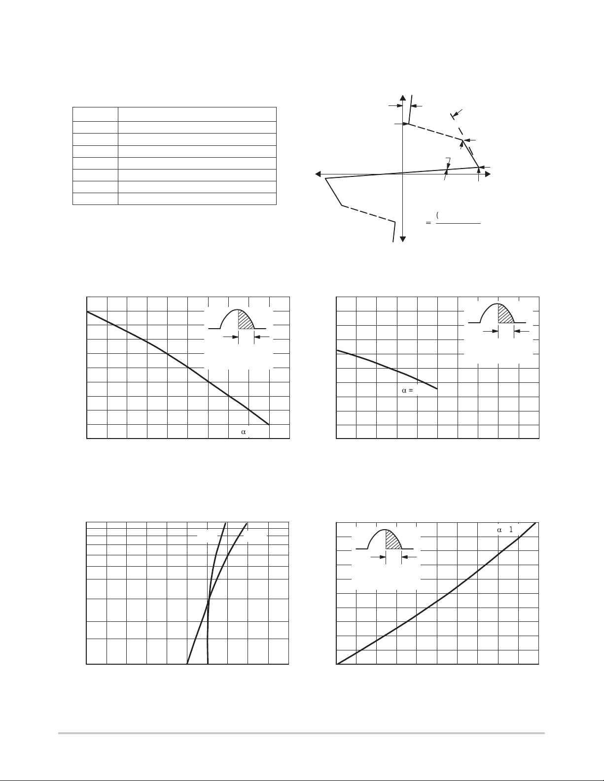
130
0
Voltage Current Characteristic of SIDAC
(Bidirectional Device)
+ Current
Symbol Parameter
I
DRM
V
DRM
V
BO
I
BO
I
H
V
TM
I
TM
°
120
110
100
90
80
, MAXIMUM ALLOWABLE CASE TEMPERATURE ( C)
C
T
Off State Leakage Current
Off State Repetitive Blocking Voltage
Breakover Voltage
Breakover Current
Holding Current
On State Voltage
Peak on State Current
0.2
0.4
I
, AVERAGE ON–STATE CURRENT (AMPS)
T(AV)
0.6
I
TM
I
H
V
TM
I
DRM
V
R
+
S
DRM
(V
(BO)–VS
(IS–I
Slope = R
V
S
V
(BO)
I
S
(BO)
)
)
S
I
(BO)
+ Voltage
CURRENT DERATING
α
α = Conduction Angle
TJ Rated = 125°C
a
= 180°
1.0
0.80
1.61.2
1.4 2.01.8
140
120
100
80
60
TEMPERATURE ( C)°
40
, MAXIMUM ALLOWABLE AMBIENT
A
T
20
0
0.2
a
= 180°
0.4
0.6
I
, AVERAGE ON–STATE CURRENT (AMPS)
T(AV)
1.00
0.8 1.2 1.4
α = Conduction Angle
α
TJ Rated = 125°C
1.6 1.8 2.
1.0
0.8
0.6
0.4
0.3
0.2
0.1
, INSTANTANEOUS ON–STATE CURRENT (AMPS)
T
I
Figure 1. Maximum Case T emperature Figure 2. Maximum Ambient T emperature
a
= 180°
25°C
0.9
VT, INSTANTANEOUS ON–STATE VOLTAGE (VOLTS)
1.0 1.10.8
125°C
1.2
1.3
1.25
1.00
0.75
0.50
0.25
, MAXIMUM AVERAGE POWER DISSIPATION (W ATTS)
AV
P
α
α = Conduction Angle
TJ Rated = 125°C
I
T(AV)
0.2 0.60
0.4 0.8
, AVERAGE ON–STATE CURRENT (AMPS)
Figure 3. T ypical Forward Voltage Figure 4. T ypical Power Dissipation
http://onsemi.com
3
1.0
Page 4

1.0
Z
q
D
0.5
where:
0.3
D
0.2
lead temperature
r(t) = normalized value of transient thermal resistance at
time, t from this figure. For example,
0.1
r(tp) = normalized value of
transient resistance at time tp.
0.05
0.03
0.02
0.01
r(t), TRANSIENT THERMAL RESIST ANCE (NORMALIZED)
MKP3V120, MKP3V240
THERMAL CHARACTERISTICS
(t) = R
JL
TJL = Ppk R
TJL = the increase in junction temperature above the
• r(t)
q
JL
[r(t)]
q
JL
t
TIME
p
10
5.00.2 0.5 1.0 2.0
Figure 5. Thermal Response
LEAD LENGTH = 1/4″
The temperature of the lead should be
measured using a thermocouple placed on the
lead as close as possible to the tie point. The
thermal mass connected to the tie point is
normally large enough so that it will not
significantly respond to heat surges generated
in the diode as a result of pulsed operation
once steady–state conditions are achieved.
Using the measured value of TL, the junction
temperature may be determined by:
TJ = TL + DT
20 50 100 200 500 1.0 k 2.0 k 5.0 k 10 k
t, TIME (ms)
JL
20 k
m
, BREAKOVER CURRENT ( A)
I
100
90
80
70
60
50
40
30
20
(BO)
10
TYPICAL CHARACTERISTICS
250
225
200
175
150
125
100
75
, HOLDING CURRENT (mA)
H
I
50
25
0
TJ, JUNCTION TEMPERATURE (°C)
40–40 –20 0 20
100–60
8060 120 140
Figure 6. T ypical Breakover Current Figure 7. T ypical Holding Current
0
–40 –20 100 140
–60
0604020
TJ, JUNCTION TEMPERATURE (°C)
80
120
http://onsemi.com
4
Page 5

MKP3V120, MKP3V240
P ACKAGE DIMENSIONS
SURMETIC 50
PLASTIC AXIAL
(No Polarity)
CASE 267–03
ISSUE D
D
1
B
K
A
2
K
NOTES:
1. DIMENSIONING AND TOLERANCING PER ANSI
Y14.5M, 1982.
2. CONTROLLING DIMENSION: INCH.
DIM MIN MAX MIN MAX
A 0.370 0.380 9.40 9.65
B 0.190 0.210 4.83 5.33
D 0.048 0.052 1.22 1.32
K 1.000 ––– 25.40 –––
STYLE 2:
NO POLARITY
MILLIMETERSINCHES
http://onsemi.com
5
Page 6

Notes
MKP3V120, MKP3V240
http://onsemi.com
6
Page 7

Notes
MKP3V120, MKP3V240
http://onsemi.com
7
Page 8

MKP3V120, MKP3V240
ON Semiconductor and are trademarks of Semiconductor Components Industries, LLC (SCILLC). SCILLC reserves the right to make changes
without further notice to any products herein. SCILLC makes no warranty , representation or guarantee regarding the suitability of its products for any particular
purpose, nor does SCILLC assume any liability arising out of the application or use of any product or circuit, and specifically disclaims any and all liability ,
including without limitation special, consequential or incidental damages. “Typical” parameters which may be provided in SCILLC data sheets and/or
specifications can and do vary in different applications and actual performance may vary over time. All operating parameters, including “Typicals” must be
validated for each customer application by customer’s technical experts. SCILLC does not convey any license under its patent rights nor the rights of others.
SCILLC products are not designed, intended, or authorized for use as components in systems intended for surgical implant into the body, or other applications
intended to support or sustain life, or for any other application in which the failure of the SCILLC product could create a situation where personal injury or
death may occur. Should Buyer purchase or use SCILLC products for any such unintended or unauthorized application, Buyer shall indemnify and hold
SCILLC and its officers, employees, subsidiaries, affiliates, and distributors harmless against all claims, costs, damages, and expenses, and reasonable
attorney fees arising out of, directly or indirectly , any claim of personal injury or death associated with such unintended or unauthorized use, even if such claim
alleges that SCILLC was negligent regarding the design or manufacture of the part. SCILLC is an Equal Opportunity/Affirmative Action Employer .
PUBLICATION ORDERING INFORMATION
NORTH AMERICA Literature Fulfillment:
Literature Distribution Center for ON Semiconductor
P.O. Box 5163, Denver, Colorado 80217 USA
Phone: 303–675–2175 or 800–344–3860 Toll Free USA/Canada
Fax: 303–675–2176 or 800–344–3867 Toll Free USA/Canada
Email: ONlit@hibbertco.com
Fax Response Line: 303–675–2167 or 800–344–3810 T oll Free USA/Canada
N. American Technical Support: 800–282–9855 Toll Free USA/Canada
EUROPE: LDC for ON Semiconductor – European Support
German Phone: (+1) 303–308–7140 (M–F 1:00pm to 5:00pm Munich Time)
Email: ONlit–german@hibbertco.com
French Phone: (+1) 303–308–7141 (M–F 1:00pm to 5:00pm Toulouse T ime)
Email: ONlit–french@hibbertco.com
English Phone: (+1) 303–308–7142 (M–F 12:00pm to 5:00pm UK Time)
Email: ONlit@hibbertco.com
EUROPEAN TOLL–FREE ACCESS*: 00–800–4422–3781
*Available from Germany, France, Italy, England, Ireland
CENTRAL/SOUTH AMERICA:
Spanish Phone: 303–308–7143 (Mon–Fri 8:00am to 5:00pm MST)
Email: ONlit–spanish@hibbertco.com
ASIA/PACIFIC : LDC for ON Semiconductor – Asia Support
Phone: 303–675–2121 (Tue–Fri 9:00am to 1:00pm, Hong Kong Time)
T oll Free from Hong Kong & Singapore:
001–800–4422–3781
Email: ONlit–asia@hibbertco.com
JAPAN: ON Semiconductor, Japan Customer Focus Center
4–32–1 Nishi–Gotanda, Shinagawa–ku, T okyo, Japan 141–0031
Phone: 81–3–5740–2745
Email: r14525@onsemi.com
ON Semiconductor Website: http://onsemi.com
For additional information, please contact your local
Sales Representative.
http://onsemi.com
8
MKP3V120/D
 Loading...