

MJW21192 (NPN),
MJW21191 (PNP)
Complementary Silicon
Plastic Power Transistors
Specifically designed for power audio output, or high power drivers
in audio amplifiers.
• DC Current Gain Specified up to 8.0 A at Temperature
• All On Characteristics at Temperature
• High SOA: 20 A, 18 V, 100 ms
• TO−247AE Package
• Pb−Free Packages are Available*
MAXIMUM RATINGS
MJW21191
CEO
CB
EB
I
C
B
P
q
q
D
stg
JC
JA
MJW21192
150 Vdc
150 Vdc
5.0 Vdc
8.0
16
2.0 Adc
125
0.65
–65 to
+150
1.0
50
Unit
Adc
W
W/_C
_C
_C/W
_C/W
Rating Symbol
Collector−Emitter Voltage V
Collector−Base Voltage V
Emitter−Base Voltage V
Collector Current − Continuous
Base Current I
Total Power Dissipation @ TC = 25_C
Derate above 25_C
Operating and Storage Junction
Temperature Range
− Peak
TJ, T
THERMAL CHARACTERISTICS
Characteristic Symbol Max Unit
Thermal Resistance, Junction to Case
Thermal Resistance, Junction to Ambient
Maximum ratings are those values beyond which device damage can occur.
Maximum ratings applied to the device are individual stress limit values (not
normal operating conditions) and are not valid simultaneously. If these limits are
exceeded, device functional operation is not implied, damage may occur and
reliability may be affected.
1000
PNP
NPN
100
R
R
http://onsemi.com
8.0 A
POWER TRANSISTORS
COMPLEMENTARY SILICON
150 V, 125 W
TO−247
CASE 340L
STYLE 3
1
2
3
MARKING DIAGRAM
MJW2119x
AYWWG
1 BASE
2 COLLECTOR
x = 1 or 2
A = Assembly Location
Y = Year
WW = Work Week
G = Pb−Free Package
ORDERING INFORMATION
3 EMITTER
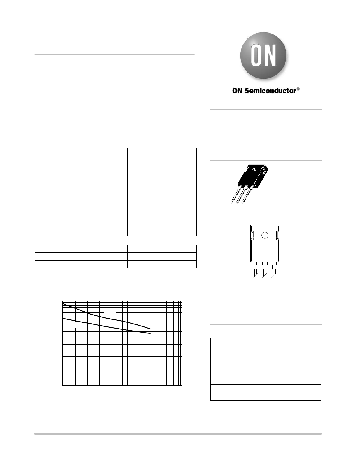
10
C, CAPACITANCE (pF)
1.0
1.0
10 100 1000
VR, REVERSE VOLTAGE (V)
Figure 1. Typical Capacitance @ 25°C
*For additional information on our Pb−Free strategy and soldering details, please
download the ON Semiconductor Soldering and Mounting Techniques
Reference Manual, SOLDERRM/D.
© Semiconductor Components Industries, LLC, 2005
June, 2005 − Rev. 2
1 Publication Order Number:
Device Package Shipping
MJW21191 TO−247 30 Units/Rail
MJW21191G TO−247
(Pb−Free)
MJW21192 TO−247 30 Units/Rail
MJW21192G TO−247
(Pb−Free)
30 Units/Rail
30 Units/Rail
MJW21192/D
MJW21192 (NPN), MJW21191 (PNP)
ELECTRICAL CHARACTERISTICS (T
= 25_C unless otherwise noted)
C
Characteristic Symbol Min Max Unit
OFF CHARACTERISTICS
Collector−Emitter Sustaining Voltage (Note 1)
(IC = 10 mAdc, IB = 0)
Collector Cutoff Current
(VCB = 250 Vdc, IE = 0)
Emitter Cutoff Current
(VBE = 5.0 Vdc, IC = 0)
ON CHARACTERISTICS (Note 1)
DC Current Gain
(IC = 4.0 Adc, VCE = 2.0 Vdc)
(IC = 8.0 Adc, VCE = 2.0 Vdc)
Collector−Emitter Saturation Voltage
(IC = 4.0 Adc, IB = 0.4 Adc)
(IC = 8.0 Adc, IB = 1.6 Adc)
Base−Emitter On Voltage
(IC = 4.0 Adc, VCE = 2.0 Vdc)
DYNAMIC CHARACTERISTICS
Current Gain − Bandwidth Product (Note 2)
(IC = 1.0 Adc, VCE = 10 Vdc, f
= 1.0 MHz)
test
1. Pulse Test: Pulse Width v 300 ms, Duty Cycle v 2.0%.
2. fT = ⎪hfe⎪• f
test
.
V
CEO(sus)
I
CES
I
EBO
h
V
CE(sat)
V
BE(on)
f
FE
Vdc
150 −
mAdc
− 10
mAdc
− 10
−
15
5.0
100
−
Vdc
−
−
1.0
2.0
− 2.0 Vdc
T
4.0 − MHz
1.0
D = 0.5
0.2
0.1
0.1
0.05
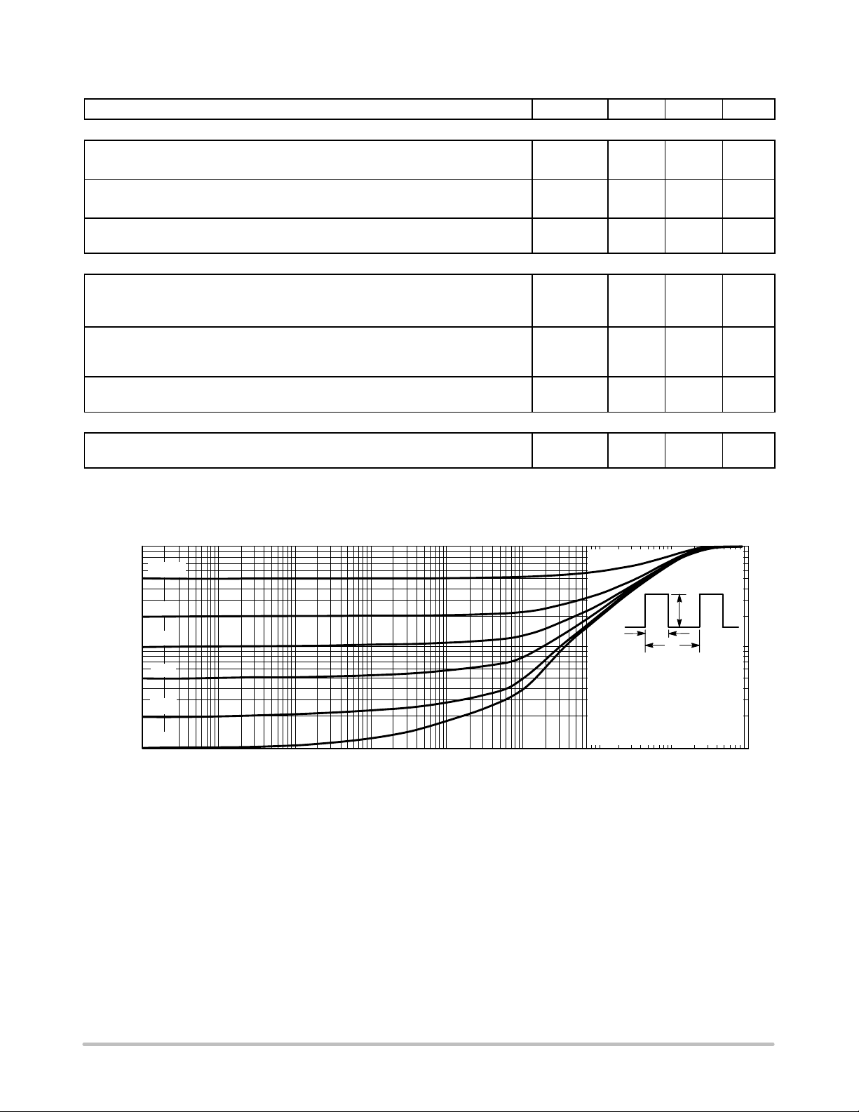
TRANSIENT THERMAL
RESISTANCE (NORMALIZED)
0.02
0.01
0.01
0.00001 0.0001 0.001 0.01 0.1 1.0 10
Figure 2. Thermal Response
There are two limitations on the power handling ability of
a transistor: average junction temperature and second
breakdown. Safe operating area curves indicate IC − V
CE
limits of the transistor that must be observed for reliable
operation, i.e., the transistor must not be subjected to greater
dissipation then the curves indicate.
DUTY
CYCLE,
D = t1/t
P
(pk)
t
1
t
2
Z
= r(t) R
θ
JC(t)
R
θ
JC
θ
JC
= 1.65°C/W MAX
D CURVES APPLY FOR POWER
PULSE TRAIN SHOWN
READ TIME AT t
T
− TC = P
J(pk)
(pk)
1
Z
θ
JC(t)
100 1000
t, TIME (s)
The data of Figures 3 and 4 is based on T
J(pk)
= 150_C;
TC is variable depending on conditions. Second breakdown
pulse limits are valid for duty cycles to 10% provided T
< 150_C. T
may be calculated from the data in
J(pk)
Figure 2. At high case temperatures, thermal limitations will
reduce the power that can be handled to values less than the
limitations imposed by second breakdown.
2
J(pk)
http://onsemi.com
2

MJW21192 (NPN), MJW21191 (PNP)
NPN — MJW21192 PNP — MJW21191
100
10
1.0
, COLLECTOR CURRENT (AMPS)
C
I
0.1
100 ms
1.0
VCE, COLLECTOR−EMITTER VOLTAGE (VOLTS)
10 1000
10ms
250ms
Figure 3. NPN — MJW21192
100
100
10
1.0
, COLLECTOR CURRENT (AMPS)
C
I
0.1
1.0
VCE, COLLECTOR−EMITTER VOLTAGE (VOLTS)
Figure 4. PNP — MJW21191
Safe Operating Area
TYPICAL CHARACTERISTICS
NPN — MJW21192 PNP — MJW21191
1000
1000
10 ms
100 ms
250 ms
10
Safe Operating Area
100
1000
100
, DC CURRENT GAIN
FE
h
1.0
100°C
25°C
10
0.01
50°C
0.1 10
IC, COLLECTOR CURRENT (AMPS)
1.0
100
100°C
100
25°C
, DC CURRENT GAIN
10
FE
h
1.0
0.01 1.0 100
Figure 5. NPN — MJW21192
V
= 2.0 V DC Current Gain
CE
50°C
0.1 10
IC, COLLECTOR CURRENT (AMPS)
Figure 6. PNP — MJW21191
V
= 2.0 V DC Current Gain
CE
http://onsemi.com
3

MJW21192 (NPN), MJW21191 (PNP)
NPN — MJW21192 PNP — MJW21191
1000
50°C
100°C
100
25°C
, DC CURRENT GAIN
10
FE
h
1.0
0.01 1.0 100
0.1 10
IC, COLLECTOR CURRENT (AMPS)
Figure 7. NPN — MJW21192
V
= 5.0 V DC Current Gain
CE
1.0
100°C
0.1
25°C
1000
50°C
100°C
100
25°C
10
FE
h , DC CURRENT GAIN
1.0
0.01 1.0 100
0.1 10
IC, COLLECTOR CURRENT (AMPS)
Figure 8. PNP — MJW21191
V
= 5.0 V DC Current Gain
CE
1.0
0.1
V, VOLTAGE (VOLTS)
0.01
V, VOLTAGE (VOLTS)
0.01
1.0
0.1
0.1
0.1
IC, COLLECTOR CURRENT (AMPS)
Figure 9. NPN — MJW21192
V
CE(sat) IC/IB
IC, COLLECTOR CURRENT (AMPS)
= 5.0
Figure 11. NPN — MJW21192
V
CE(sat) IC/IB
= 10
100°C
25°C
V, VOLTAGE (VOLTS)
100°C
25°C
101.0
0.01
IC, COLLECTOR CURRENT (AMPS)
100.1 1.0
Figure 10. PNP — MJW21191
V
CE(sat) IC/IB
10
1.0
0.1
V, VOLTAGE (VOLTS)
100°C
25°C
101.0
0.01
0.1
IC, COLLECTOR CURRENT (AMPS)
= 5.0
101.0
Figure 12. PNP — MJW21191
SPACE
V
CE(sat) IC/IB
= 10
http://onsemi.com
4

MJW21192 (NPN), MJW21191 (PNP)
CE
BE(on)
CE
BE(on)
NPN — MJW21192 PNP — MJW21191
V, VOLTAGE (VOLTS)
1.0
0.1
10
50°C
25°C
100°C
0.01 0.1
IC, COLLECTOR CURRENT (AMPS)
100.001 1.0
Figure 13. NPN — MJW21192
V
= 2.0 V V
Curve
V, VOLTAGE (VOLTS)
1.0
0.1
10
50°C
25°C
100°C
0.01 0.1
IC, COLLECTOR CURRENT (AMPS)
100.001 1.0
Figure 14. PNP — MJW21191
V
= 2.0 V V
Curve
http://onsemi.com
5

MJW21192 (NPN), MJW21191 (PNP)
PACKAGE DIMENSIONS
TO−247
CASE 340L−02
ISSUE D
−T−
−B−
U
N
A
123
C
E
L
4
−Q−
0.63 (0.025)MTB
P
−Y−
K
F
2 PL
G
W
D
3 PL
0.25 (0.010)MYQ
J
H
S
NOTES:
1. DIMENSIONING AND TOLERANCING PER ANSI
Y14.5M, 1982.
2. CONTROLLING DIMENSION: MILLIMETER.
DIM MIN MAX MIN MAX
A 20.32 21.08 0.800 8.30
B 15.75 16.26 0.620 0.640
C 4.70 5.30 0.185 0.209
D 1.00 1.40 0.040 0.055
M
E 2.20 2.60 0.087 0.102
F 1.65 2.13 0.065 0.084
G 5.45 BSC 0.215 BSC
H 1.50 2.49 0.059 0.098
J 0.40 0.80 0.016 0.031
K 20.06 20.83 0.790 0.820
L 5.40 6.20 0.212 0.244
N 4.32 5.49 0.170 0.216
P −−− 4.50 −−− 0.177
Q 3.55 3.65 0.140 0.144
U 6.15 BSC 0.242 BSC
W 2.87 3.12 0.113 0.123
STYLE 3:
PIN 1. BASE
2. COLLECTOR
3. EMITTER
4. COLLECTOR
INCHESMILLIMETERS
ON Semiconductor and are registered trademarks of Semiconductor Components Industries, LLC (SCILLC). SCILLC reserves the right to make changes without further notice
to any products herein. SCILLC makes no warranty, representation or guarantee regarding the suitability of its products for any particular purpose, nor does SCILLC assume any liability
arising out of the application or use of any product or circuit, and specifically disclaims any and all liability, including without limitation special, consequential or incidental damages.
“Typical” parameters which may be provided in SCILLC data sheets and/or specifications can and do vary in different applications and actual performance may vary over time. All
operating parameters, including “Typicals” must be validated for each customer application by customer’s technical experts. SCILLC does not convey any license under its patent rights
nor the rights of others. SCILLC products are not designed, intended, or authorized for use as components in systems intended for surgical implant into the body, or other applications
intended to support or sustain life, or for any other application in which the failure of the SCILLC product could create a situation where personal injury or death may occur. Should
Buyer purchase or use SCILLC products for any such unintended or unauthorized application, Buyer shall indemnify and hold SCILLC and its officers, employees, subsidiaries, affiliates,
and distributors harmless against all claims, costs, damages, and expenses, and reasonable attorney fees arising out of, directly or indirectly, any claim of personal injury or death
associated with such unintended or unauthorized use, even if such claim alleges that SCILLC was negligent regarding the design or manufacture of the part. SCILLC is an Equal
Opportunity/Affirmative Action Employer. This literature is subject to all applicable copyright laws and is not for resale in any manner.
PUBLICATION ORDERING INFORMATION
LITERATURE FULFILLMENT:
Literature Distribution Center for ON Semiconductor
P.O. Box 61312, Phoenix, Arizona 85082−1312 USA
Phone: 480−829−7710 or 800−344−3860 Toll Free USA/Canada
Fax: 480−829−7709 or 800−344−3867 Toll Free USA/Canada
Email: orderlit@onsemi.com
N. American Technical Support: 800−282−9855 Toll Free
USA/Canada
Japan: ON Semiconductor, Japan Customer Focus Center
2−9−1 Kamimeguro, Meguro−ku, Tokyo, Japan 153−0051
Phone: 81−3−5773−3850
http://onsemi.com
ON Semiconductor Website: http://onsemi.com
Order Literature: http://www.onsemi.com/litorder
For additional information, please contact your
local Sales Representative.
MJW21192/D
6
 Loading...