

查询MJW18020供应商
MJW18020
Preferred Devices
NPN Silicon Power
Transistors High Voltage
Planar
The MJW18020 planar High Voltage Power Transistor is
specifically Designed for motor control applications, high power
supplies and UPS’s for which the high reproducibility of DC and
Switching parameters minimizes the dead time in bridge
configurations.
Mains features include:
• High and Excellent Gain Linearity
• Fast and Very Tight Switching Times Parameters t
• Very Stable Leakage Current due to the Planar Structure
• High Reliability
and t
si
fi
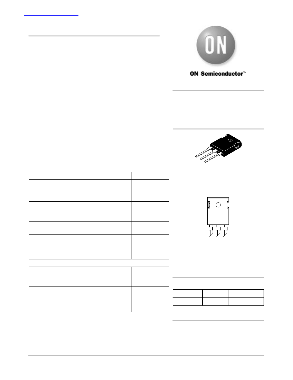
http://onsemi.com
30 AMPERES
1000 VOLTS BV
450 VOLTS BV
250 WATTS
CES
CEO
MAXIMUM RATINGS
Rating Symbol Value Unit
Collector–Emitter Sustaining Voltage V
Collector–Base Breakdown Voltage V
Collector–Base Voltage V
Emitter–Base Voltage V
Collector Current – Continuous
Base Current – Continuous
Total Power Dissipation @ TC = 25C
Derate Above 25C
Operating and Storage Junction
Temperature Range
– Peak (Note 1.)
– Peak (Note 1.)
TJ, T
THERMAL CHARACTERISTICS
Characteristic Symbol Max Unit
Thermal Resistance,
Junction–to–Case
Thermal Resistance,
Junction–to–Ambient
Maximum Lead Temperature for Soldering
Purposes: 1/8” from Case for 5 Seconds
1. Pulse Test: Pulse Width = 5 s, Duty Cycle ≤ 10%.
R
R
CEO
CES
CBO
EBO
I
C
I
B
P
θ
θ
T
D
JC
JA
L
stg
450 Vdc
1000 Vdc
1000 Vdc
9.0 Vdc
30
45
6.0
10
250
2.0
–65 to
+150
0.5 C/W
50 C/W
275 C
Adc
Adc
Watts
W/C
C
1
2
3
TO–247
CASE 340K
STYLE 3
MARKING DIAGRAM
MJW
18020
LLYWW
1 BASE
2 COLLECTOR
MJW18020= Device Code
LL = Location Code
Y = Year
WW = Work Week
3 EMITTER
ORDERING INFORMATION
Device Package Shipping
MJW18020 TO–247
30 Units/Rail
Semiconductor Components Industries, LLC, 2002
January , 2002 – Rev. 0
Preferred devices are recommended choices for future use
and best overall value.
1 Publication Order Number:
MJW180203/D
MJW18020
(
C
,
B1 B2
,
ELECTRICAL CHARACTERISTICS (T
= 25°C unless otherwise noted)
C
Characteristic Symbol Min Typ Max Unit
OFF CHARACTERISTICS
Collector–Emitter Sustaining Voltage
= 100 mAdc, IB = 0)
(I
C
Collector Cutoff Current
(V
CE
= Rated V
CEO
, IB = 0)
Collector Cutoff Current (VCE = Rated V
Emitter Cutoff Current
= 9 Vdc, IC = 0)
(V
CE
, VEB = 0)
CES
(T
C
= 125°C)
V
CEO(sus)
I
CEO
I
CES
I
EBO
ON CHARACTERISTICS
DC Current Gain (I
= 3 Adc, VCE = 5 Vdc)
C
= 10 Adc VCE = 2 Vdc)
(I
C
(I
= 20 Adc VCE = 2 Vdc)
C
(I
= 10 mAdc VCE = 5 Vdc)
C
Base–Emitter Saturation Voltage (IC = 10 Adc, IB = 2 Adc)
(I
= 20 Adc, IB = 4 Adc)
C
Collector–Emitter Saturation Voltage
= 10 Adc, IB = 2 Adc)
(I
C
(I
= 20 Adc, IB = 4 Adc)
C
(T
= 125°C)
C
= 125°C)
(T
C
= 125°C)
(T
C
= 125°C)
(T
C
= 125°C)
(T
C
h
V
BE(sat)
V
CE(sat)
FE
DYNAMIC CHARACTERISTICS
Current Gain Bandwidth Product
(I
= 1 Adc, VCE = 10 Vdc, f
C
test
Output Capacitance
= 10 Vdc, IE = 0, f
(V
CB
= 1 MHz)
test
Input Capacitance
(V
= 8.0)
EB
= 1 MHz)
f
T
C
ob
C
ib
SWITCHING CHARACTERISTICS: Resistive Load (D.C. = 10%, Pulse Width = 70 µs)
Turn–On Time
Storage Time t
Fall Time t
Turn–Off Time t
Turn–On Time
Storage Time
Fall Time t
Turn–Off Time t
SWITCHING CHARACTERISTICS: Inductive Load (V
Fall Time
Storage Time
Crossover Time
Fall Time
Storage Time
Crossover Time
(IC = 10 Adc, IB1 = IB2 = 2 Adc,
Vcc = 125 V)
(IC= 20 Adc, IB1 = IB2 = 4 Adc,
Vcc = 125 V)
= 300 V , Vcc = 15 V, L = 200 µH)
clamp
(IC = 10 Adc, IB1 = IB2 = 2 Adc)
(IC = 20 Adc, IB1 = IB2 = 4 Adc)
t
On
s
f
Off
t
On
t
s
f
Off
t
fi
t
si
t
c
t
fi
t
si
t
c
450 – – Vdc
– – 100 µAdc
– – 100
µAdc
500
– – 100 µAdc
14
–
8
5
5.5
4
14
– 0.97
1.15
30
16
14
9
7
25
34
–
–
–
–
–
1.25
1.5
Vdc
Vdc
–
–
–
–
0.2
0.3
0.5
0.9
0.6
–
1.5
2.0
– 13 – MHz
– 300 500 pF
– 7000 9000 pF
– 540 750 ns
– 4.75 6 µs
– 380 500 ns
– 5.2 6.5 µs
– 965 1200 ns
– 2.9 3.5 µs
– 350 500 ns
– 3.25 4 µs
– 142 250 ns
– 4.75 6 µs
– 320 500 ns
– 350 500 ns
– 3.0 3.5 µs
– 500 750 ns
http://onsemi.com
2
MJW18020
0
0
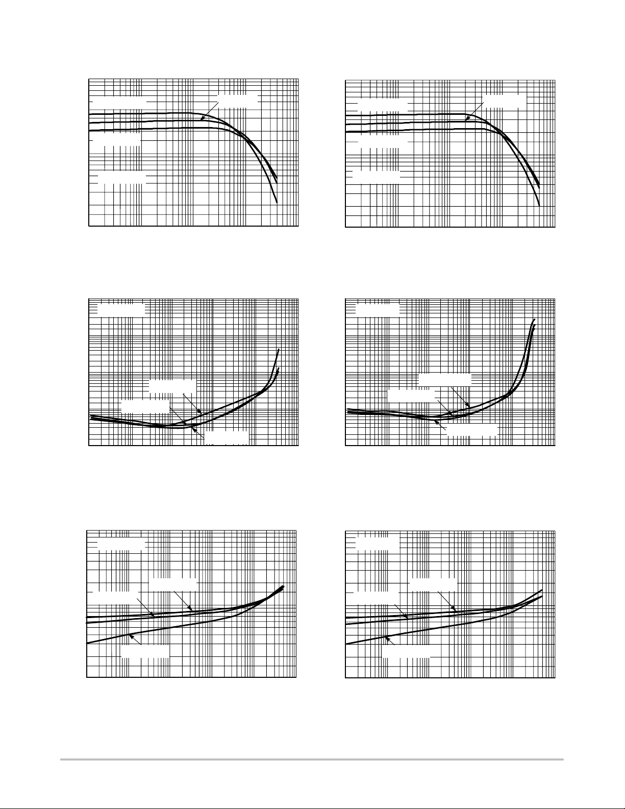
TYPICAL CHARACTERISTICS
100
TJ = 125°C
TJ = –20°C
10
, DC CURRENT GAIN
H
VCE = 2.0 V VCE = 5.0 V
FE
1.0
0.01 0.1 1.0 10
I
, COLLECTOR CURRENT (A)
C
TJ = 25°C
Figure 1. DC Current Gain, VCE = 2.0 V
100.0
10.0
1.0
TJ = –20°C
, VOLTAGE (VOLTS)
0.1
CE
V
0.0
0.001 0.01 0.1 1.0 10 100
TJ = 125°C
I
, COLLECTOR CURRENT (A)
C
TJ = 25°C
100
100
TJ = 125°C
TJ = –20°C
10
, DC CURRENT GAIN
FE
H
1.0
0.01 0.1 1.0 10
IC, COLLECTOR CURRENT (A)
TJ = 25°C
Figure 2. DC Current Gain, VCE = 5.0 V
100.0
Ic/Ib = 10Ic/Ib = 5.0
10.0
1.0
, VOLTAGE (VOLTS)
0.1
CE
V
0.0
0.001 0.01 0.1 1.0 10 10
TJ = 125°C
IC, COLLECTOR CURRENT (A)
TJ = –20°C
TJ = 25°C
100
Figure 3. Typical Collector–Emitter Saturation
Voltage, I
10.0
TJ = –20°C
TJ = 25°C
1.0
, VOLTAGE (VOLTS)
BE
V
0.1
0.001 0.01 0.1 1.0 10 100
TJ = 125°C
IC, COLLECTOR CURRENT (A)
C/IB
= 5.0
Figure 5. Typical Base–Emitter Saturation
Voltage, I
C/IB
= 5.0
10.0
1.0
, VOLTAGE (VOLTS)
BE
V
0.1
0.001 0.01 0.1 1.0 10 10
http://onsemi.com
3
Figure 4. Typical Collector–Emitter Saturation
Voltage, IC/IB = 10
Ic/Ib = 10Ic/Ib = 5.0
TJ = –20°C
TJ = 25°C
TJ = 125°C
IC, COLLECTOR CURRENT (A)
Figure 6. Typical Base–Emitter Saturation
Voltage, IC/IB = 10

MJW18020
TYPICAL CHARACTERISTICS
100000
10000
C, CAPACITANCE (pF)
C
ib
1000
C
ob
100
1 10 100
VCE, COLLECTOR–EMITTER VOLTAGE (VOLTS)
Figure 7. T ypical Capacitance
40
30
100.00
1.0 s
DC
10.00
5 ms
1.00
0.10
, COLLECTOR CURRENT (AMPS)
C
I
0.01
10 100 1000
VCE, COLLECTOR–EMITTER VOLTAGE (VOLTS)
1 ms
Extended SOA
10 s
Figure 8. Forward Bias Safe Operating Area
TC 125°C
I
> 4
c/Ib
= 500 H
L
C
20
–1.5 V
10
, COLLECTOR CURRENT (AMPS)
C
I
0
0 200 400 600 800 1000
VCE, COLLECTOR–EMITTER VOLTAGE (VOLTS)
VBE = 0 V
–5 V
Figure 9. Reverse Bias Safe Operating Area
http://onsemi.com
4

MJW18020
PACKAGE DIMENSIONS
TO–247
CASE 340K–01
ISSUE C
0.25 (0.010)MTB
A
K
0.25 (0.010)MYQ
–Q–
M
P
U
F
D
S
–B–
123
G
–T–
E
C
4
L
R
–Y–
V
H
J
NOTES:
1. DIMENSIONING AND TOLERANCING PER ANSI
Y14.5M, 1982.
2. CONTROLLING DIMENSION: MILLIMETER.
DIM MIN MAX MIN MAX
A 19.7 20.3 0.776 0.799
B 15.3 15.9 0.602 0.626
C 4.7 5.3 0.185 0.209
D 1.0 1.4 0.039 0.055
E 1.27 REF 0.050 REF
F 2.0 2.4 0.079 0.094
G 5.5 BSC 0.216 BSC
H 2.2 2.6 0.087 0.102
J 0.4 0.8 0.016 0.031
K 14.2 14.8 0.559 0.583
L 5.5 NOM 0.217 NOM
P 3.7 4.3 0.146 0.169
Q 3.55 3.65 0.140 0.144
R 5.0 NOM 0.197 NOM
U 5.5 BSC 0.217 BSC
V 3.0 3.4 0.118 0.134
STYLE 3:
PIN 1. BASE
2. COLLECTOR
3. EMITTER
4. COLLECTOR
INCHESMILLIMETERS
http://onsemi.com
5

Notes
MJW18020
http://onsemi.com
6

Notes
MJW18020
http://onsemi.com
7

MJW18020
ON Semiconductor and are trademarks of Semiconductor Components Industries, LLC (SCILLC). SCILLC reserves the right to make changes
without further notice to any products herein. SCILLC makes no warranty, representation or guarantee regarding the suitability of its products for any particular
purpose, nor does SCILLC assume any liability arising out of the application or use of any product or circuit, and specifically disclaims any and all liability,
including without limitation special, consequential or incidental damages. “Typical” parameters which may be provided in SCILLC data sheets and/or
specifications can and do vary in different applications and actual performance may vary over time. All operating parameters, including “Typicals” must be
validated for each customer application by customer’s technical experts. SCILLC does not convey any license under its patent rights nor the rights of others.
SCILLC products are not designed, intended, or authorized for use as components in systems intended for surgical implant into the body, or other applications
intended to support or sustain life, or for any other application in which the failure of the SCILLC product could create a situation where personal injury or
death may occur. Should Buyer purchase or use SCILLC products for any such unintended or unauthorized application, Buyer shall indemnify and hold
SCILLC and its officers, employees, subsidiaries, affiliates, and distributors harmless against all claims, costs, damages, and expenses, and reasonable
attorney fees arising out of, directly or indirectly, any claim of personal injury or death associated with such unintended or unauthorized use, even if such claim
alleges that SCILLC was negligent regarding the design or manufacture of the part. SCILLC is an Equal Opportunity/Affirmative Action Employer.
PUBLICATION ORDERING INFORMATION
Literature Fulfillment:
Literature Distribution Center for ON Semiconductor
P.O. Box 5163, Denver, Colorado 80217 USA
Phone: 303–675–2175 or 800–344–3860 Toll Free USA/Canada
Fax: 303–675–2176 or 800–344–3867 Toll Free USA/Canada
Email: ONlit@hibbertco.com
N. American Technical Support: 800–282–9855 Toll Free USA/Canada
http://onsemi.com
JAPAN: ON Semiconductor, Japan Customer Focus Center
4–32–1 Nishi–Gotanda, Shinagawa–ku, Tokyo, Japan 141–0031
Phone: 81–3–5740–2700
Email: r14525@onsemi.com
ON Semiconductor Website: http://onsemi.com
For additional information, please contact your local
Sales Representative.
MJW18020/D
8
 Loading...