

Page 1
MC100EP16VC
3.3V / 5VECL Differential
Receiver/Driver with High
Gain and Enable Output
The EP16VC is a differential receiver/driver. The device is
functionally equivalent to the EP16 and LVEP16 devices but with high
gain and enable output.
The EP16VC provides an EN
data input (D) signal in a way that provides glitchless gating of the
QHG and QHG
When the EN
outputs.
signal is LOW, the input is passed to the outputs and
the data output equals the data input. When the data input is HIGH and
goes HIGH, it will force the QHG LOW and the QHG HIGH on the
EN
next negative transition of the data input. If the data input is LOW
when the EN
and Q
goes HIGH, the next data transition to a HIGH is ignored
remains LOW and QHG remains HIGH. The next positive
HG
transition of the data input is not passed on to the data outputs under
these conditions. The Q
HG
state as long as the EN
influence on the Q
this output whether EN
output and the data input is passed on (inverted) to
is HIGH or LOW. This configuration is ideal
for crystal oscillator applications where the oscillator can be free
running and gated on and off synchronously without adding extra
counts to the output.
The VBB/D pin is internally dedicated and available for differential
interconnect. V
decouple V
/D may rebias AC coupled inputs. When used,
BB
/D and VCC via a 0.01 F capacitor and limit current
BB
sourcing or sinking to 1.5 mA. When not used, V
open.
The 100 Series contains temperature compensation.
• 310 ps Typical Prop Delay Q, 380 ps Typical Prop Delay QHG, QHG
• Gain > 200
• Maximum Frequency > 3 GHz Typical
• PECL Mode Operating Range: V
with V
EE
= 0 V
• NECL Mode Operating Range: V
with V
= −3.0 V to −5.5 V
EE
• Open Input Default State
• Q
Output Will Default LOW with D Inputs Open or at V
HG
• V
Output
BB
input which is synchronized with the
and QHG outputs remain in their disabled
input is held HIGH. The EN input has no
/D should be left
BB
= 3.0 V to 5.5 V
CC
= 0 V
CC
EE
http://onsemi.com
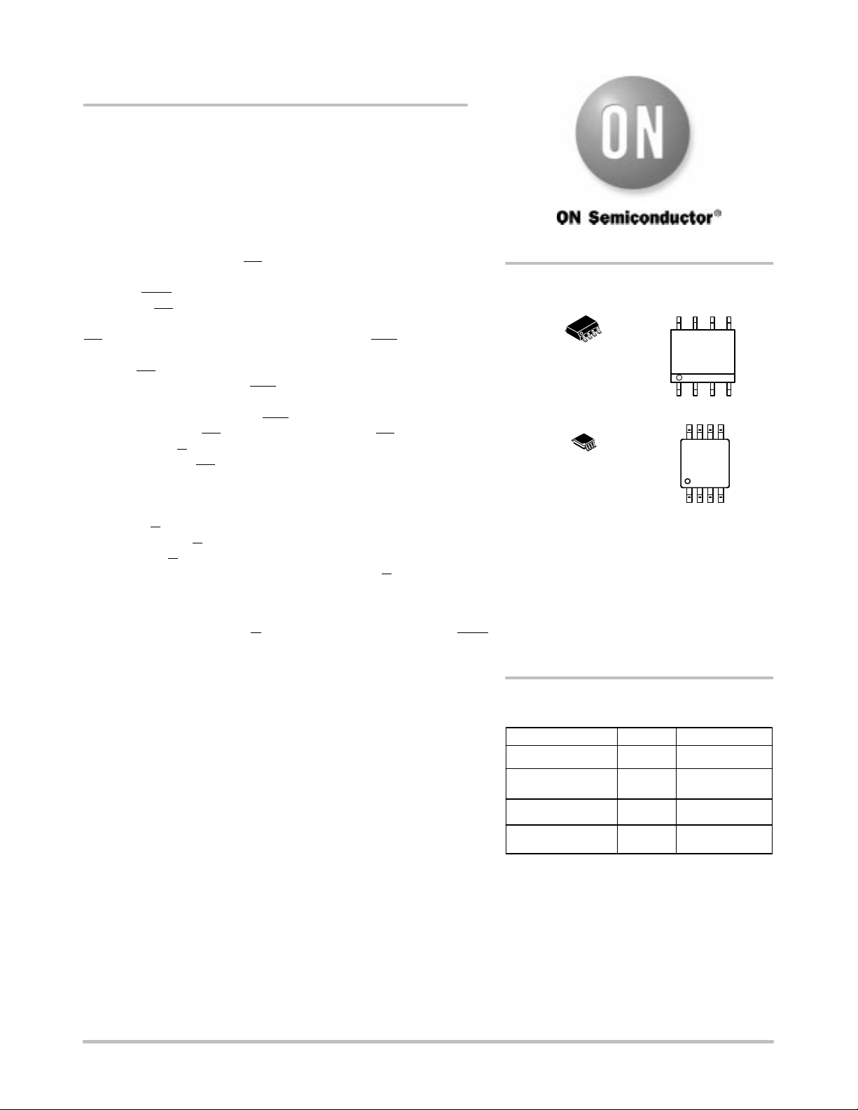
MARKING DIAGRAMS*
8
1
SO−8
D SUFFIX
CASE 751
8
1
TSSOP−8
DT SUFFIX
CASE 948R
K = MC100
A = Assembly Location
L = Wafer Lot
Y = Year
W= Work Week
*For additional information, see Application Note
AND8002/D
ORDERING INFORMATION
Device Package Shipping
MC100EP16VCD SO−8 98 Units/Rail
MC100EP16VCDR2 SO−8 2500 Tape & Reel
MC100EP16VCDT TSSOP−8 100 Units/Rail
8
KEP66
ALYW
1
8
KP66
ALYW
1
Semiconductor Components Industries, LLC, 2003
September, 2003− Rev. 2
MC100EP16VCDTR2 TSSOP−8 2500 Tape & Reel
1 Publication Order Number:
MC100EP16VC/D
Page 2
MC100EP16VC
VBB/D
1
Q
D
2
3
OE
Q
LEN
V
BB
45
EN
LATCH
D
78Q
6
V
CC
HG
Q
HG
V
EE
Figure 1. 8−Lead Pinout (Top View) and Logic Diagram
ATTRIBUTES
Characteristics Value
Internal Input Pulldown Resistor 75 k
Internal Input Pullup Resistor N/A
ESD Protection Human Body Model
Charged Device Model
Moisture Sensitivity, Indefinite Time Out of Drypack (Note 1) Level 1
Flammability Rating Oxygen Index: 28 to 34 UL 94 V−0 @ 0.125 in
Transistor Count 167 Devices
Meets or exceeds JEDEC Spec EIA/JESD78 IC Latchup Test
1. For additional information, see Application Note AND8003/D.
PIN DESCRIPTION
PIN FUNCTION
D* ECL Data Input
Q
Q
, Q
HG
HG
EN
* ECL Enable Input
/D Reference Voltage Output / ECL Data Input
V
BB
V
CC
V
EE
* Pins will default LOW when left open.
Machine Model
ECL Data Output
ECL High Gain Data Outputs
Positive Supply
Negative Supply
> 4 kV
> 200 V
> 2 kV
MAXIMUM RATINGS (Note 2)
Symbol
V
CC
V
EE
V
I
I
out
I
BB
PECL Mode Power Supply VEE = 0 V 6 V
NECL Mode Power Supply VCC = 0 V −6 V
PECL Mode Input Voltage
NECL Mode Input Voltage
Output Current Continuous
VBB Sink/Source ± 1.5 mA
TA Operating Temperature Range −40 to +85 °C
T
stg
JA
JC
JA
JC
T
sol
Storage Temperature Range −65 to +150 °C
Thermal Resistance (Junction−to−Ambient) 0 LFPM
Thermal Resistance (Junction−to−Case) std bd 8 SOIC 41 to 44 °C/W
Thermal Resistance (Junction−to−Ambient) 0 LFPM
Thermal Resistance (Junction−to−Case) std bd 8 TSSOP 41 to 44 °C/W
Wave Solder <2 to 3 sec @ 248°C 265 °C
2. Maximum Ratings are those values beyond which device damage may occur.
Parameter Condition 1 Condition 2 Rating Units
VEE = 0 V
VCC = 0 V
Surge
500 LFPM
500 LFPM
VI V
CC
VI V
EE
8 SOIC
8 SOIC
8 TSSOP
8 TSSOP
6
−6
50
100
190
130
185
140
mA
mA
°C/W
°C/W
°C/W
°C/W
http://onsemi.com
2
V
V
Page 3
MC100EP16VC
100EP DC CHARACTERISTICS, PECL V
= 3.3 V, VEE = 0 V (Note 3)
CC
−40°C 25°C 85°C
Symbol Characteristic
I
EE
V
OH
V
OL
V
IH
V
IL
V
BB
V
IHCMR
I
IH
I
IL
NOTE: EP circuits are designed to meet the DC specifications shown in the above table after thermal equilibrium has been established. The
3. Input and output parameters vary 1:1 with V
4. All loading with 50 to V
5. V
IHCMR
input signal.
100EP DC CHARACTERISTICS, PECL V
Power Supply Current 25 36 45 30 40 50 32 42 52 mA
Output HIGH Voltage (Note 4) 2105 2230 2355 2105 2230 2355 2105 2230 2355 mV
Output LOW Voltage (Note 4) 1305 1430 1555 1305 1430 1555 1305 1430 1555 mV
Input HIGH Voltage (Single−Ended) 2075 2420 2075 2420 2075 2420 mV
Input LOW Voltage (Single−Ended) 1355 1675 1355 1675 1355 1675 mV
Output Voltage Reference 1725 1825 1925 1700 1800 1900 1675 1775 1875 mV
Input HIGH Voltage Common Mode
Range (Differential) (Note 5)
Input HIGH Current 150 150 150 A
Input LOW Current D 0.5 0.5 0.5 A
circuit is in a test socket or mounted on a printed circuit board and transverse airflow greater than 500 lfpm is maintained.
−2.0 volts.
min varies 1:1 with VEE, V
CC
IHCMR
CC
max varies 1:1 with VCC. The V
CC
Min Typ Max Min Typ Max Min Typ Max
2.0 3.3 2.0 3.3 2.0 3.3 V
. VEE can vary +0.3 V to −2.2 V.
range is referenced to the most positive side of the differential
IHCMR
= 5.0 V, VEE = 0 V (Note 6)
Unit
−40°C 25°C 85°C
Symbol Characteristic
I
EE
V
OH
V
OL
V
IH
V
IL
V
BB
V
IHCMR
I
IH
I
IL
NOTE: EP circuits are designed to meet the DC specifications shown in the above table after thermal equilibrium has been established. The
6. Input and output parameters vary 1:1 with V
7. All loading with 50 to V
8. V
IHCMR
input signal.
Power Supply Current 25 36 45 30 40 50 32 42 52 mA
Output HIGH Voltage (Note 7) 3805 3930 4055 3805 3930 4055 3805 3930 4055 mV
Output LOW Voltage (Note 7) 3005 3130 3255 3005 3130 3255 3005 3130 3255 mV
Input HIGH Voltage (Single−Ended) 3775 4120 3775 4120 3775 4120 mV
Input LOW Voltage (Single−Ended) 3055 3375 3055 3375 3055 3375 mV
Output Voltage Reference 3425 3525 3625 3400 3500 3600 3375 3475 3575 mV
Input HIGH Voltage Common Mode
Range (Differential) (Note 8)
Input HIGH Current 150 150 150 A
Input LOW Current D 0.5 0.5 0.5 A
circuit is in a test socket or mounted on a printed circuit board and transverse airflow greater than 500 lfpm is maintained.
−2.0 volts.
min varies 1:1 with VEE, V
CC
IHCMR
CC
max varies 1:1 with VCC. The V
Min Typ Max Min Typ Max Min Typ Max
2.0 5.0 2.0 5.0 2.0 5.0 V
. VEE can vary +2.0 V to −0.5 V.
range is referenced to the most positive side of the differential
IHCMR
Unit
100EP DC CHARACTERISTICS, NECL V
= 0 V; V
CC
= −5.5 V to −3.0 V (Note 9)
EE
−40°C 25°C 85°C
Symbol Characteristic
I
EE
V
OH
V
OL
V
IH
V
IL
V
BB
V
IHCMR
I
IH
I
IL
NOTE: EP circuits are designed to meet the DC specifications shown in the above table after thermal equilibrium has been established. The
9. Input and output parameters vary 1:1 with V
10.All loading with 50 to V
11. V
IHCMR
input signal.
Power Supply Current 25 36 45 30 40 50 32 42 52 mA
Output HIGH Voltage (Note 10) −1195 −1070 −945 −1195 −1070 −945 −1195 −1070 −945 mV
Output LOW Voltage (Note 10) −1995 −1870 −1745 −1995 −1870 −1745 −1995 −1870 −1745 mV
Input HIGH Voltage (Single−Ended) −1225 −880 −1225 −880 −1225 −880 mV
Input LOW Voltage (Single−Ended) −1945 −1625 −1945 −1625 −1945 −1625 mV
Output Voltage Reference −1575 −1475 −1375 −1600 −1500 −1400 −1625 −1525 −1425 mV
Input HIGH Voltage Common Mode
Range (Differential) (Note 11)
Input HIGH Current 150 150 150 A
Input LOW Current D 0.5 0.50 0.5 A
circuit is in a test socket or mounted on a printed circuit board and transverse airflow greater than 500 lfpm is maintained.
−2.0 volts.
min varies 1:1 with VEE, V
CC
max varies 1:1 with VCC. The V
IHCMR
Min Typ Max Min Typ Max Min Typ Max
VEE+2.0 0.0 VEE+2.0 0.0 VEE+2.0 0.0 V
.
CC
range is referenced to the most positive side of the differential
IHCMR
Unit
http://onsemi.com
3
Page 4
MC100EP16VC
AC CHARACTERISTICS V
= 0 V; VEE = −3.0 V to −5.5 V or VCC = 3.0 V to 5.5 V; V
CC
= 0 V (Note 12)
EE
−40°C 25°C 85°C
Symbol Characteristic
f
t
t
max
PLH
PHL
Maximum Frequency
(See Figure 2 F
,
Propagation Delay (Differential) Q
max
/JITTER)
(Differential) QHG, QHG
(Single−Ended) Q
(Single−Ended) QHG, QHG
t
S
t
H
t
SKEW
t
JITTER
V
PP
t
r
t
f
Setup Time EN = L to D
Hold Time EN = L to D
Duty Cycle Skew (Note 13) 5.0 20 5.0 20 5.0 20 ps
RMS Random Clock Jitter
(See Figure 2 F
max
/JITTER)
Input Voltage Swing HG
(Differential Configuration) Q25150
Output Rise/Fall Times Q
(20% − 80%) QHG, QHG
EN =H to D501001560
EN =H to D
Min Typ Max Min Typ Max Min Typ Max
> 3 > 3 > 3 GHz
200
250
250
300
1005050
280
360
330
410
15
350
450
400
500
250
300
300
350
310
380
360
430
50
100540
1005040
20
400
500
450
550
275
325
325
375
340
430
390
480
50
1001810
100
50
20
425
525
475
575
5
0.2 < 1 0.2 < 1 0.2 < 1 ps
800
800
20070300
130
1200
120025150
400
25080350
220
800
800
150
1200
120025150
450
250
240
100
800
800
350
170
1200
1200
500
270
Unit
ps
ps
ps
mV
ps
12.Measured using a 750 mV source, 50% duty cycle clock source. All loading with 50 to VCC−2.0 V.
13.Skew is measured between outputs under identical transitions. Duty cycle skew is defined only for differential operation when the delays
are measured from the cross point of the inputs to the cross point of the outputs.
http://onsemi.com
4
Page 5

MC100EP16VC
ЙЙЙЙЙЙЙ
ЙЙЙЙЙЙЙ
ЙЙЙЙЙЙЙ
ЙЙЙЙЙЙЙ
Single−Ended Input
900
800
700
(mV)
600
500
OUTpp
V
400
300
200
100
0
0 500 1000 1500 2000 2500 3000 3500 4000
FREQUENCY (MHz)
Figure 2. F
/Jitter for QHG, QHG Output
max
900
800
700
(mV)
600
500
OUTpp
V
400
300
200
100
0
0 500 1000 1500 2000 2500 3000 3500 4000
FREQUENCY (MHz)
9
8
7
6
5
4
3
2
1
9
8
7
6
5
4
3
2
1
ps (RMS)
OUT
JITTER
ps (RMS)
OUT
JITTER
Figure 3. F
http://onsemi.com
/Jitter for Q Output
max
5
Page 6

MC100EP16VC
Differential Inputs
900
800
700
(mV)
600
500
OUTpp
V
400
300
200
100
0
0 500 1000 1500 2000 2500 3000
FREQUENCY (MHz)
Figure 4. F
/Jitter for QHG, QHG Output
max
900
800
700
(mV)
600
500
OUTpp
V
400
300
200
100
0
0 500 1000 1500 2000 2500 3000
FREQUENCY (MHz)
9
8
7
6
5
4
3
2
1
9
8
7
6
5
4
3
2
1
ps (RMS)
OUT
JITTER
ps (RMS)
OUT
JITTER
Figure 5. F
http://onsemi.com
/Jitter for Q Output
max
6
Page 7

Driver
Device
MC100EP16VC
QD
Receiver
Device
Q D
50
V
TT
50
V
TT
V
=
CC
− 2.0 V
Figure 6. Typical Termination for Output Driver and Device Evaluation
(Refer to Application Note AND8020 − Termination of ECL Logic Devices.)
Resource Reference of Application Notes
AN1404 − ECLinPS Circuit Performance at Non−Standard VIH Levels
AN1405 − ECL Clock Distribution Techniques
AN1406 − Designing with PECL (ECL at +5.0 V)
AN1504 − Metastability and the ECLinPS Family
AN1568 − Interfacing Between LVDS and ECL
AN1650 − Using Wire−OR Ties in ECLinPS Designs
AN1672 − The ECL Translator Guide
AND8001 − Odd Number Counters Design
AND8002 − Marking and Date Codes
AND8009 − ECLinPS Plus Spice I/O Model Kit
AND8020 − Termination of ECL Logic Devices
For an updated list of Application Notes, please see our website at http://onsemi.com.
http://onsemi.com
7
Page 8

−Y−
−Z−
MC100EP16VC
PACKAGE DIMENSIONS
SO−8
D SUFFIX
PLASTIC SOIC PACKAGE
CASE 751−07
M
ISSUE AA
M
Y
N
X 45
K
M
−X−
A
58
B
1
S
0.25 (0.010)
4
G
C
SEATING
PLANE
0.10 (0.004)
H
D
0.25 (0.010) Z
M
Y
SXS
NOTES:
1. DIMENSIONING AND TOLERANCING PER ANSI
Y14.5M, 1982.
2. CONTROLLING DIMENSION: MILLIMETER.
3. DIMENSION A AND B DO NOT INCLUDE MOLD
PROTRUSION.
4. MAXIMUM MOLD PROTRUSION 0.15 (0.006) PER
SIDE.
5. DIMENSION D DOES NOT INCLUDE DAMBAR
PROTRUSION. ALLOWABLE DAMBAR
PROTRUSION SHALL BE 0.127 (0.005) TOTAL IN
EXCESS OF THE D DIMENSION AT MAXIMUM
MATERIAL CONDITION.
6. 751−01 THRU 751−06 ARE OBSOLETE. NEW
STANDAARD IS 751−07
MILLIMETERS
DIMAMIN MAX MIN MAX
4.80 5.00 0.189 0.197
B 3.80 4.00 0.150 0.157
C 1.35 1.75 0.053 0.069
D 0.33 0.51 0.013 0.020
G 1.27 BSC 0.050 BSC
H 0.10 0.25 0.004 0.010
J
J 0.19 0.25 0.007 0.010
K 0.40 1.27 0.016 0.050
M 0 8 0 8
N 0.25 0.50 0.010 0.020
S 5.80 6.20 0.228 0.244
INCHES
http://onsemi.com
8
Page 9

MC100EP16VC
PACKAGE DIMENSIONS
TSSOP−8
DT SUFFIX
PLASTIC TSSOP PACKAGE
CASE 948R−02
ISSUE A
−T−
L
0.10 (0.004)
SEATING
PLANE
8x REFK
S
U0.15 (0.006) T
2X L/2
85
0.10 (0.004) V
M
B
PIN 1
IDENT
S
U0.15 (0.006) T
1
−U−
4
A
−V−
S
U
T
S
0.25 (0.010)
M
F
DETAIL E
C
D
G
DETAIL E
−W−
NOTES:
1. DIMENSIONING AND TOLERANCING PER ANSI
Y14.5M, 1982.
2. CONTROLLING DIMENSION: MILLIMETER.
3. DIMENSION A DOES NOT INCLUDE MOLD FLASH.
PROTRUSIONS OR GATE BURRS. MOLD FLASH
OR GATE BURRS SHALL NOT EXCEED 0.15
(0.006) PER SIDE.
4. DIMENSION B DOES NOT INCLUDE INTERLEAD
FLASH OR PROTRUSION. INTERLEAD FLASH OR
PROTRUSION SHALL NOT EXCEED 0.25 (0.010)
PER SIDE.
5. TERMINAL NUMBERS ARE SHOWN FOR
REFERENCE ONLY.
6. DIMENSION A AND B ARE TO BE DETERMINED
AT DATUM PLANE −W−.
DIM MIN MAX MIN MAX
A 2.90 3.10 0.114 0.122
B 2.90 3.10 0.114 0.122
C 0.80 1.10 0.031 0.043
D 0.05 0.15 0.002 0.006
F 0.40 0.70 0.016 0.028
G 0.65 BSC 0.026 BSC
K 0.25 0.40 0.010 0.016
L 4.90 BSC 0.193 BSC
M 0 6 0 6
INCHESMILLIMETERS
http://onsemi.com
9
Page 10

MC100EP16VC
ON Semiconductor and are registered trademarks of Semiconductor Components Industries, LLC (SCILLC). SCILLC reserves the right to make
changes without further notice to any products herein. SCILLC makes no warranty, representation or guarantee regarding the suitability of its products for any
particular purpose, nor does SCILLC assume any liability arising out of the application or use of any product or circuit, and specifically disclaims any and all
liability, including without limitation special, consequential or incidental damages. “Typical” parameters which may be provided in SCILLC data sheets and/or
specifications can and do vary in different applications and actual performance may vary over time. All operating parameters, including “Typicals” must be
validated for each customer application by customer’s technical experts. SCILLC does not convey any license under its patent rights nor the rights of others.
SCILLC products are not designed, intended, or authorized for use as components in systems intended for surgical implant into the body, or other applications
intended to support or sustain life, or for any other application in which the failure of the SCILLC product could create a situation where personal injury or death
may occur. Should Buyer purchase or use SCILLC products for any such unintended or unauthorized application, Buyer shall indemnify and hold SCILLC
and its officers, employees, subsidiaries, affiliates, and distributors harmless against all claims, costs, damages, and expenses, and reasonable attorney fees
arising out of, directly or indirectly, any claim of personal injury or death associated with such unintended or unauthorized use, even if such claim alleges that
SCILLC was negligent regarding the design or manufacture of the part. SCILLC is an Equal Opportunity/Affirmative Action Employer.
PUBLICATION ORDERING INFORMATION
Literature Fulfillment:
Literature Distribution Center for ON Semiconductor
P.O. Box 5163, Denver, Colorado 80217 USA
Phone: 303−675−2175 or 800−344−3860 Toll Free USA/Canada
Fax: 303−675−2176 or 800−344−3867 Toll Free USA/Canada
Email: ONlit@hibbertco.com
N. American Technical Support: 800−282−9855 Toll Free USA/Canada
http://onsemi.com
JAPAN: ON Semiconductor, Japan Customer Focus Center
2−9−1 Kamimeguro, Meguro−ku, Tokyo, Japan 153−0051
Phone: 81−3−5773−3850
Email: r14525@onsemi.com
ON Semiconductor Website: http://onsemi.com
For additional information, please contact your local
Sales Representative.
MC100EP16VC/D
10
Page 11

WWW.ALLDATASHEET.COM
Copyright © Each Manufacturing Company.
All Datasheets cannot be modified without permission.
This datasheet has been download from :
www.AllDataSheet.com
100% Free DataSheet Search Site.
Free Download.
No Register.
Fast Search System.
www.AllDataSheet.com
 Loading...