


查询MC100E137FNG供应商
MC10E137, MC100E137
5 VECL 8-Bit Ripple Counter
Description
The MC10E/100E137 is a very high speed binary ripple counter. The
two least significant bits were designed with very fast edge rates while
the more significant bits maintain standard ECLinPS™ output edge
rates. This allows the counter to operate at very high frequencies while
maintaining a moderate power dissipation level.
The device is ideally suited for multiple frequency clock generation
as well as a counter in a high performance ATE time measurement
board.
Both asynchronous and synchronous enables are available to
maximize the device’s flexibility for various applications. The
asynchronous enable input, A_Start, when asserted enables the counter
while overriding any synchronous enable signals. The E137 features
XORed enable inputs, EN1 and EN2, which are synchronous to the
CLK input. When only one synchronous enable is asserted the counter
becomes disabled on the next CLK transition; all outputs remain in the
previous state poised for the other synchronous enable or A_Start to be
asserted to re-enable the counter. Asserting both synchronous enables
causes the counter to become enabled on the next transition of the CLK.
If EN1 (or EN2) and CLK edges are coincident, sufficient delay has
been inserted in the CLK path (to compensate for the XOR gate delay
and the internal D-flip flop setup time) to insure that the synchronous
enable signal is clocked correctly, hence, the counter is disabled.
All input pins left open will be pulled LOW via an input pulldown
resistor. Therefore, do not leave the differential CLK inputs open.
Doing so causes the current source transistor of the input clock gate to
become saturated, thus upsetting the internal bias regulators and
jeopardizing the stability of the device.
The asynchronous Master Reset resets the counter to an all zero state
upon assertion.
The VBB pin, an internally generated voltage supply, is available to
this device only. For single-ended input conditions, the unused
differential input is connected to VBB as a switching reference voltage.
VBB may also rebias AC coupled inputs. When used, decouple VBB and
VCC via a 0.01 mF capacitor and limit current sourcing or sinking to
0.5 mA. When not used, VBB should be left open.
The 100 Series contains temperature compensation.
http://onsemi.com
PLCC−28
FN SUFFIX
CASE 776
MARKING DIAGRAM*
1
MCxxxE137FNG
AWLYYWW
xxx = 10 or 100
A = Assembly Location
WL = Wafer Lot
YY = Year
WW = Work Week
G = Pb−Free Package
*For additional marking information, refer to
Application Note AND8002/D.
ORDERING INFORMATION
See detailed ordering and shipping information in the package
dimensions section on page 7 of this data sheet.
Features
• Differential Clock Input and Data Output Pins
• V
Output for Single-Ended Use
BB
• Synchronous and Asynchronous Enable Pins
• Asynchronous Master Reset
• PECL Mode Operating Range: V
with VEE = 0 V
• NECL Mode Operating Range: V
with VEE = −4.2 V to −5.7 V
= 4.2 V to 5.7 V
CC
= 0 V
CC
• Internal Input 50 kW Pull−down Resistors
• Transistor Count = 330 devices
*For additional information on our Pb−Free strategy and soldering details, please download the ON Semiconductor Soldering and Mounting
Techniques Reference Manual, SOLDERRM/D.
© Semiconductor Components Industries, LLC, 2006
November, 2006 − Rev. 8
• ESD Protection: Human Body Model: > 2 kV,
Machine Model: > 200 V
• Meets or Exceeds JEDEC Spec EIA/JESD78 IC
Latchup Test
• Moisture Sensitivity Level: Pb = 1; Pb−Free = 3
For Additional Information, see Application Note
AND8003/D
• Flammability Rating: UL 94 V−0 @ 0.125 in,
Oxygen Index: 28 to 34
• Pb−Free Packages are Available*
1 Publication Order Number:
MC10E137/D

MC10E137, MC100E137
Q6
V
CCO
22
21
8
A_Start
EN1
EN2
V
CLK
CLK
V
BB
Q7 Q6
25
26
27
28
1
EE
2
3
4
5
MR
* All VCC and V
Warning: All VCC, V
Q7
24
23
Pinout: 28-Lead PLCC
(Top View)
7
6
V
Q0
CCO
pins are tied together on the die.
CCO
, and VEE pins must be externally
CCO
connected to Power Supply to guarantee proper operation.
Figure 1. 28−Lead Pinout
Q5
Q1Q1Q0
Q5
19
20
18
Q4
17
Q4
16
V
CC
Q3
15
Q3
14
Q2
13
12
Q2
Table 1. PIN DESCRIPTION
PIN FUNCTION
CLK, CLK
Q0-Q7, Q0-Q7
A_Start
EN1, EN2
MR
V
BB
VCC, V
CCO
V
EE
ECL Differential Clock Inputs
ECL Differential Q Outputs
ECL Asynchronous Enable Input
ECL Synchronous Enable Inputs
Asynchronous Master Reset
Reference Voltage Output
Positive Supply
Negative Supply
11109
V
CCO
A_Start
EN1
EN2
CLK
CLK
V
BB
MR
D
CLK
CLK
R
Q0 Q0 Q1 Q1
Q7 Q7
Q
Q
CLK
CLK
D
Q
Q
R
CLK
CLK
D
Q
Q
CLK
CLK
Q
Q
D
R
R
Figure 2. Logic Diagram
http://onsemi.com
2

MC10E137, MC100E137
Table 2. SEQUENTIAL TRUTH TABLE
Function EN1 EN2 A_Start MR CLK Q7 Q6 Q5 Q4 Q3 Q2 Q1 Q0
Reset X X X H X L L L L L L L L
Count L
L
L
Stop H
H
Asynch Start H
H
L
Count L
L
L
Stop L
L
Synch Start H
H
H
Stop H
H
Count L
L
L
Reset X X X H X L L L L L L L L
Z = Low to High Transition
L
L
L
L
L
L
L
L
L
L
L
H
H
H
H
H
L
L
L
L
L
L
L
L
L
L
H
H
H
L
L
L
L
L
L
L
L
L
L
L
L
L
L
L
L
L
L
L
L
L
L
L
L
L
L
L
L
L
L
L
L
L
L
Z
Z
Z
Z
Z
Z
Z
Z
Z
Z
Z
Z
Z
Z
Z
Z
Z
Z
Z
Z
Z
L
L
L
L
L
L
L
L
L
L
L
L
L
L
L
L
L
L
L
L
L
L
L
L
L
L
L
L
L
L
L
L
L
L
L
L
L
L
L
L
L
L
L
L
L
L
L
L
L
L
L
L
L
L
L
L
L
L
L
L
L
L
L
L
L
L
L
L
L
L
L
L
L
L
L
L
L
L
L
L
L
L
L
L
L
L
L
L
L
L
L
L
L
H
H
H
H
H
H
H
H
H
H
H
H
L
L
L
L
L
H
H
H
H
L
L
L
L
L
L
H
H
H
H
H
H
L
H
H
H
H
L
L
H
H
L
L
L
L
H
H
L
L
L
L
H
H
H
L
H
H
H
L
H
L
H
L
H
H
H
L
H
L
L
L
H
L
H
Table 3. MAXIMUM RATINGS
Symbol Parameter Condition 1 Condition 2 Rating Unit
V
CC
V
EE
V
I
I
out
T
A
T
stg
q
JA
q
JC
V
EE
T
sol
Stresses exceeding Maximum Ratings may damage the device. Maximum Ratings are stress ratings only. Functional operation above the
Recommended Operating Conditions is not implied. Extended exposure to stresses above the Recommended Operating Conditions may affect
device reliability.
PECL Mode Power Supply VEE = 0 V 8 V
NECL Mode Power Supply VCC = 0 V −8 V
PECL Mode Input Voltage
NECL Mode Input Voltage
Output Current Continuous
VEE = 0 V
VCC = 0 V
Surge
VI v V
VI w V
CC
EE
6
−6
50
100
V
V
mA
mA
Operating Temperature Range 0 to +85 °C
Storage Temperature Range −65 to +150 °C
Thermal Resistance (Junction−to−Ambient) 0 lfpm
500 lfpm
PLCC−28
PLCC−28
63.5
43.5
°C/W
°C/W
Thermal Resistance (Junction−to−Case) Standard Board PLCC−28 22 to 26 °C/W
PECL Operating Range
NECL Operating Range
Wave Solder Pb
Pb−Free
4.2 to 5.7
−5.7 to −4.2
265
265
V
V
°C
http://onsemi.com
3

MC10E137, MC100E137
Table 4. 10E SERIES PECL DC CHARACTERISTICS V
= 5.0 V; VEE = 0.0 V (Note 1)
CCx
0°C 25°C 85°C
Symbol Characteristic
I
EE
V
OH
V
OL
V
IH
V
IL
V
BB
V
IHCMR
Power Supply Current 121 145 121 145 121 145 mA
Output HIGH Voltage (Note 2) 3980 40704160 4020 4105 4190 4090 4185 4280 mV
Output LOW Voltage (Note 2) 3050 3210 3370 3050 3210 3370 3050 3227 3405 mV
Input HIGH Voltage (Single−Ended) 3830 3995 4160 3870 4030 4190 3940 4110 4280 mV
Input LOW Voltage (Single−Ended) 3050 3285 3520 3050 3285 3520 3050 3302 3555 mV
Output Voltage Reference 3.62 3.73 3.65 3.75 3.69 3.81 V
Input HIGH Voltage Common Mode
Range (Differential Configuration)
Min Typ Max Min Typ Max Min Typ Max Unit
2.2 4.6 2.2 4.6 2.2 4.6 V
(Note 3)
I
IH
I
IL
Input HIGH Current 150 150 150
Input LOW Current 0.5 0.3 0.5 0.25 0.3 0.2
mA
mA
NOTE: Device will meet the specifications after thermal equilibrium has been established when mounted in a test socket or printed circuit
board with maintained transverse airflow greater than 500 lfpm. Electrical parameters are guaranteed only over the declared
operating temperature range. Functional operation of the device exceeding these conditions is not implied. Device specification limit
values are applied individually under normal operating conditions and not valid simultaneously.
1. Input and output parameters vary 1:1 with VCC. VEE can vary −0.46 V / +0.06 V.
2. Outputs are terminated through a 50 W resistor to VCC − 2.0 V.
3. V
Table 5. 10E SERIES NECL DC CHARACTERISTICS V
min varies 1:1 with VEE, max varies 1:1 with VCC.
IHCMR
= 0.0 V; VEE = −5.0 V (Note 4)
CCx
0°C 25°C 85°C
Symbol Characteristic
I
EE
V
OH
V
OL
V
IH
V
IL
V
BB
V
IHCMR
Power Supply Current 121 145 121 145 121 145 mA
Output HIGH Voltage (Note 5) −1020 −930 −840 −980 −895 −810 −910 −815 −720 mV
Output LOW Voltage (Note 5) −1950 −1790 −1630 −1950 −1790 −1630 −1950 −1773 −1595 mV
Input HIGH Voltage (Single−Ended) −1170 −1005 −840 −1130 −970 −810 −1060 −890 −720 mV
Input LOW Voltage (Single−Ended) −1950 −1715 −1480 −1950 −1715 −1480 −1950 −1698 −1445 mV
Output Voltage Reference −1.38 −1.27 −1.35 −1.25 −1.31 −1.19 V
Input HIGH Voltage Common Mode
Range (Differential Configuration)
Min Typ Max Min Ty p Max Min Ty p Max
Unit
−2.8 −0.4 −2.8 −0.4 −2.8 −0.4 V
(Note 6)
I
IH
I
IL
Input HIGH Current 150 150 150
Input LOW Current 0.5 0.3 0.5 0.065 0.3 0.2
mA
mA
NOTE: Device will meet the specifications after thermal equilibrium has been established when mounted in a test socket or printed circuit
board with maintained transverse airflow greater than 500 lfpm. Electrical parameters are guaranteed only over the declared
operating temperature range. Functional operation of the device exceeding these conditions is not implied. Device specification limit
values are applied individually under normal operating conditions and not valid simultaneously.
4. Input and output parameters vary 1:1 with VCC. VEE can vary −0.46 V / +0.06 V.
5. Outputs are terminated through a 50 W resistor to VCC − 2.0 V.
6. V
min varies 1:1 with VEE, max varies 1:1 with VCC.
IHCMR
http://onsemi.com
4

MC10E137, MC100E137
Table 6. 100E SERIES PECL DC CHARACTERISTICS V
= 5.0 V; VEE = 0.0 V (Note 7)
CCx
0°C 25°C 85°C
Symbol Characteristic
I
EE
V
OH
V
OL
V
IH
V
IL
V
BB
V
IHCMR
Power Supply Current 121 145 121 145 139 167 mA
Output HIGH Voltage (Note 8) 3975 4050 4120 3975 4050 4120 3975 4050 4120 mV
Output LOW Voltage (Note 8) 3190 3295 3380 3190 3255 3380 3190 3260 3380 mV
Input HIGH Voltage (Single−Ended) 3835 3975 4120 3835 3975 4120 3835 3975 4120 mV
Input LOW Voltage (Single−Ended) 3190 3355 3525 3190 3355 3525 3190 3355 3525 mV
Output Voltage Reference 3.62 3.73 3.62 3.74 3.62 3.74 V
Input HIGH Voltage Common Mode
Range (Differential Configuration)
Min Ty p Max Min Typ Max Min Typ Max
Unit
2.2 4.6 2.2 4.6 2.2 4.6 V
(Note 9)
I
IH
I
IL
Input HIGH Current 150 150 150
Input LOW Current 0.5 0.3 0.5 0.25 0.5 0.2
mA
mA
NOTE: Device will meet the specifications after thermal equilibrium has been established when mounted in a test socket or printed circuit
board with maintained transverse airflow greater than 500 lfpm. Electrical parameters are guaranteed only over the declared
operating temperature range. Functional operation of the device exceeding these conditions is not implied. Device specification limit
values are applied individually under normal operating conditions and not valid simultaneously.
7. Input and output parameters vary 1:1 with VCC. VEE can vary −0.46 V / +0.8 V.
8. Outputs are terminated through a 50 W resistor to VCC − 2.0 V.
9. V
Table 7. 100E SERIES NECL DC CHARACTERISTICS V
min varies 1:1 with VEE, max varies 1:1 with VCC.
IHCMR
= 0.0 V; VEE = −5.0 V (Note 10)
CCx
0°C 25°C 85°C
Symbol Characteristic
I
EE
V
OH
V
OL
V
IH
V
IL
V
BB
V
IHCMR
Power Supply Current 121 145 121 145 139 167 mA
Output HIGH Voltage (Note 11) −1025 −950 −880 −1025 −950 −880 −1025 −950 −880 mV
Output LOW Voltage (Note 11) −1810 −1705 −1620 −1810 −1745 −1620 −1810 −1740 −1620 mV
Input HIGH Voltage (Single−Ended)
Input LOW Voltage (Single−Ended)
Output Voltage Reference −1.38 −1.27 −1.38 −1.26 −1.38 −1.26 V
Input HIGH Voltage Common
Mode Range (Differential Configu-
Min Typ Max Min Typ Max Min Ty p Max
Unit
−1165 −1025 −880 −1165 −1025 −880 −1165 −1025 −880 mV
−1810 −1645 −1475 −1810 −1645 −1475 −1810 −1645 −1475 mV
−3.8 −0.4 −3.8 −0.4 −3.8 −0.4 V
ration) (Note 12)
I
IH
I
IL
Input HIGH Current 150 150 150
Input LOW Current 0.5 0.3 0.5 0.25 0.5 0.2
mA
mA
NOTE: Device will meet the specifications after thermal equilibrium has been established when mounted in a test socket or printed circuit
board with maintained transverse airflow greater than 500 lfpm. Electrical parameters are guaranteed only over the declared
operating temperature range. Functional operation of the device exceeding these conditions is not implied. Device specification limit
values are applied individually under normal operating conditions and not valid simultaneously.
10.Input and output parameters vary 1:1 with VCC. VEE can vary −0.46 V / +0.8 V.
11.Outputs are terminated through a 50 W resistor to VCC − 2.0 V.
12.V
min varies 1:1 with VEE, max varies 1:1 with VCC.
IHCMR
http://onsemi.com
5

MC10E137, MC100E137
Table 8. AC CHARACTERISTICS V
Symbol Characteristic
f
COUNT
t
PLH
t
PHL
t
s
t
h
t
RR
t
PW
V
PP
t
JITTER
t
r
t
f
Maximum Count Frequency 1800 2200 1800 2200 1800 2200 MHz
Propagation Delay to Output
A_Start to Q0
Setup Time (EN1, EN2) 0 −150 0 −150 0 −150 ps
Hold Time (EN1, EN2) 300 150 300 150 300 150 ps
Reset Recovery Time
Minimum Pulse Width
CLK, MR, A_Start 400 400 400
Input Voltage Swing CLK/CLK
(Differential Configuration) (Note 14)
Random Clock Jitter (RMS) < 1 < 1 < 1 ps
Rise/Fall Times (20%−80%)
= 5.0 V; VEE = 0.0 V or V
CCx
= 0.0 V; VEE = −5.0 V (Note 13)
CCx
0°C 25°C 85°C
Min Ty p Max Min Typ Max Min Typ Max
CLK to Q0
CLK to Q1
CLK to Q2
CLK to Q3
CLK to Q4
CLK to Q5
CLK to Q6
CLK to Q7
MR to Q0
1300
1600
1950
2275
2625
2950
3250
3575
950
700
1700
2025
2425
2750
3125
3450
3775
4075
1325
1000
2150
2500
2925
3350
3750
4150
4450
4800
1700
1300
1300
1600
1950
2275
2625
2950
3250
3575
950
700
1700
2050
2450
2775
3150
3475
3800
4125
1325
1000
2150
2500
2925
3350
3750
4150
4450
4800
1700
1300
1350
1650
2025
2350
2700
3050
3375
3700
950
700
1750
2100
2500
2850
3225
3550
3925
4250
1325
1000
MR, A_Start 400 200 400 200 400 200
0.25 1.0 0.25 1.0 0.25 1.0 V
Q0,Q1
Q2 to Q7
150
275
400
600
150
275
400
600
150
275
Unit
ps
2200
2550
3000
3425
3825
4250
4600
4950
1700
1300
ps
ps
ps
400
600
NOTE: Device will meet the specifications after thermal equilibrium has been established when mounted in a test socket or printed circuit
board with maintained transverse airflow greater than 500 lfpm. Electrical parameters are guaranteed only over the declared
operating temperature range. Functional operation of the device exceeding these conditions is not implied. Device specification limit
values are applied individually under normal operating conditions and not valid simultaneously.
13.10 Series: VEE can vary −0.46 V / +0.06 V.
100 Series: VEE can vary −0.46 V / +0.8 V.
14.Minimum input swing for which AC parameters are guaranteed. Full DC ECL output swings will be generated with only 50 mV input swings.
http://onsemi.com
6

MC10E137, MC100E137
Zo = 50 W
Zo = 50 W
50 W 50 W
V
VTT = VCC − 2.0 V
TT
Receiver
Device
Driver
Device
QD
Q D
Figure 3. Typical Termination for Output Driver and Device Evaluation
(See Application Note AND8020/D − Termination of ECL Logic Devices.)
ORDERING INFORMATION
Device Package Shipping
MC10E137FN PLCC−28 37 Units / Rail
MC10E137FNG PLCC−28
(Pb−Free)
MC10E137FNR2 PLCC−28 500 / Tape & Reel
MC10E137FNR2G PLCC−28
(Pb−Free)
MC100E137FN PLCC−28 37 Units / Rail
MC100E137FNG PLCC−28
(Pb−Free)
MC100E137FNR2 PLCC−28 500 / Tape & Reel
MC100E137FNR2G PLCC−28
(Pb−Free)
†For information on tape and reel specifications, including part orientation and tape sizes, please refer to our Tape and Reel Packaging
Specifications Brochure, BRD8011/D.
37 Units / Rail
500 / Tape & Reel
37 Units / Rail
500 / Tape & Reel
†
Resource Reference of Application Notes
AN1405/D − ECL Clock Distribution Techniques
AN1406/D − Designing with PECL (ECL at +5.0 V)
AN1503/D −
AN1504/D − Metastability and the ECLinPS Family
AN1568/D − Interfacing Between LVDS and ECL
AN1672/D − The ECL Translator Guide
AND8001/D − Odd Number Counters Design
AND8002/D − Marking and Date Codes
AND8020/D − Termination of ECL Logic Devices
AND8066/D − Interfacing with ECLinPS
AND8090/D − AC Characteristics of ECL Devices
ECLinPSt I/O SPiCE Modeling Kit
http://onsemi.com
7
MC10E137, MC100E137
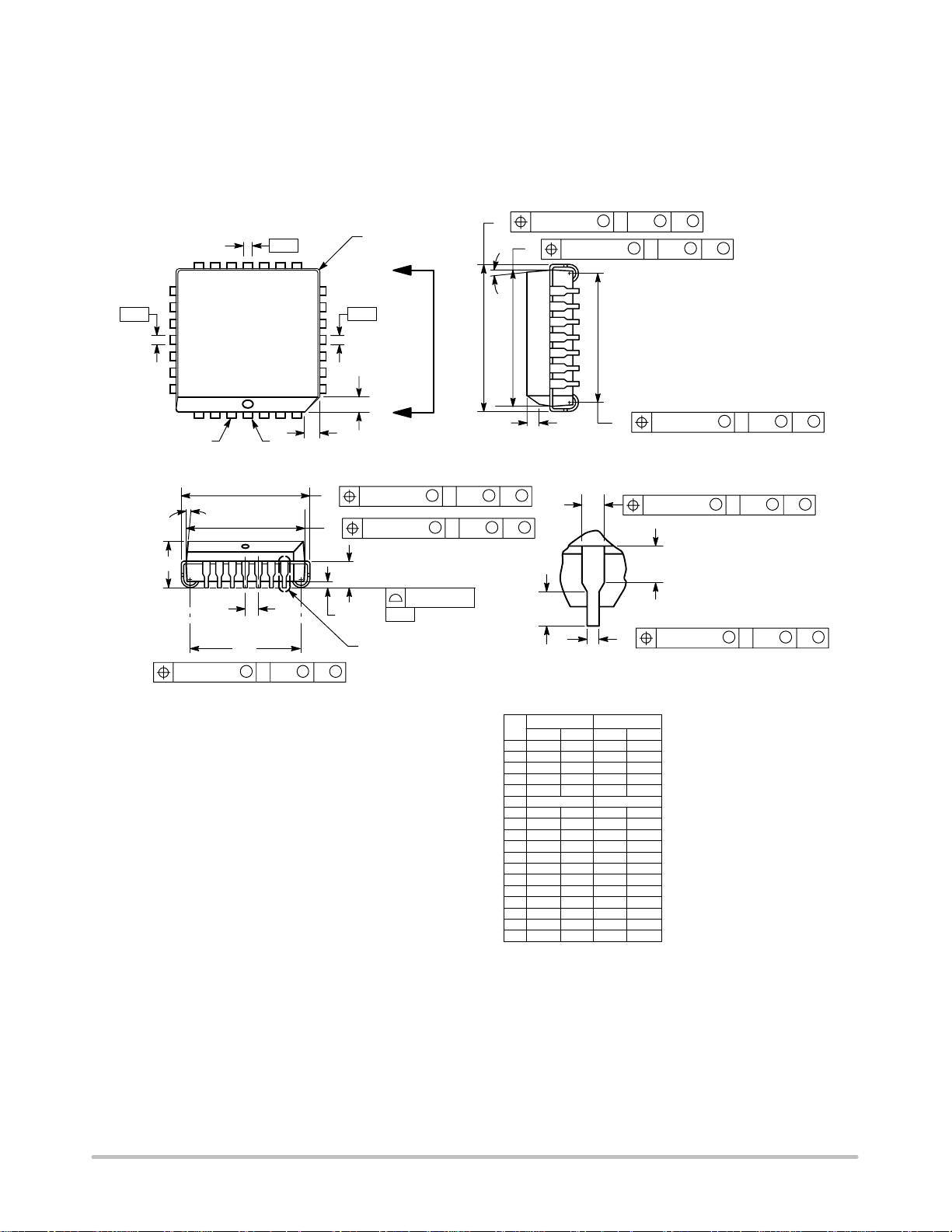
PACKAGE DIMENSIONS
PLCC−28
FN SUFFIX
PLASTIC PLCC PACKAGE
CASE 776−02
ISSUE E
−L−
−N−
28 1
Z
C
G
G1
S
0.010 (0.250) N
L−M
T
S
L−M
T
M
S
S
L−M
T
S
Y BRK
0.007 (0.180) N
B
0.007 (0.180) N
U
M
D
Z
−M−
W
D
V
0.010 (0.250) N
G1X
S
S
L−M
T
S
VIEW D−D
A
0.007 (0.180) N
0.007 (0.180) N
R
E
M
M
S
L−M
T
L−M
T
S
S
S
H
0.007 (0.180) N
M
S
L−M
T
S
K1
0.004 (0.100)
SEATING
J
−T−
PLANE
VIEW S
S
S
K
VIEW S
0.007 (0.180) N
F
M
S
L−M
T
S
NOTES:
1. DATUMS −L−, −M−, AND −N− DETERMINED
WHERE TOP OF LEAD SHOULDER EXITS
PLASTIC BODY AT MOLD PARTING LINE.
2. DIMENSION G1, TRUE POSITION TO BE
MEASURED AT DATUM −T−, SEATING PLANE.
3. DIMENSIONS R AND U DO NOT INCLUDE
MOLD FLASH. ALLOWABLE MOLD FLASH IS
0.010 (0.250) PER SIDE.
4. DIMENSIONING AND TOLERANCING PER
ANSI Y14.5M, 1982.
5. CONTROLLING DIMENSION: INCH.
6. THE PACKAGE TOP MAY BE SMALLER THAN
THE PACKAGE BOTTOM BY UP TO 0.012
(0.300). DIMENSIONS R AND U ARE
DETERMINED AT THE OUTERMOST
EXTREMES OF THE PLASTIC BODY
EXCLUSIVE OF MOLD FLASH, TIE BAR
BURRS, GATE BURRS AND INTERLEAD
FLASH, BUT INCLUDING ANY MISMATCH
BETWEEN THE TOP AND BOTTOM OF THE
PLASTIC BODY.
7. DIMENSION H DOES NOT INCLUDE DAMBAR
PROTRUSION OR INTRUSION. THE DAMBAR
PROTRUSION(S) SHALL NOT CAUSE THE H
DIMENSION TO BE GREATER THAN 0.037
(0.940). THE DAMBAR INTRUSION(S) SHALL
NOT CAUSE THE H DIMENSION TO BE
SMALLER THAN 0.025 (0.635).
DIM MIN MAX MIN MAX
A 0.485 0.495 12.32 12.57
B 0.485 0.495 12.32 12.57
C 0.165 0.180 4.20 4.57
E 0.090 0.110 2.29 2.79
F 0.013 0.019 0.33 0.48
G 0.050 BSC 1.27 BSC
H 0.026 0.032 0.66 0.81
J 0.020 −−− 0.51 −−−
K 0.025 −−− 0.64 −−−
R 0.450 0.456 11.43 11.58
U 0.450 0.456 11.43 11.58
V 0.042 0.048 1.07 1.21
W 0.042 0.048 1.07 1.21
X 0.042 0.056 1.07 1.42
Y −−− 0.020 −−− 0.50
Z 2 10 2 10
__ __
G1 0.410 0.430 10.42 10.92
K1 0.040 −−− 1.02 −−−
MILLIMETERSINCHES
http://onsemi.com
8

MC10E137, MC100E137
ECLinPS is a trademark of Semiconductor Components Industries, LLC (SCILLC).
ON Semiconductor and are registered trademarks of Semiconductor Components Industries, LLC (SCILLC). SCILLC reserves the right to make changes without further notice
to any products herein. SCILLC makes no warranty, representation or guarantee regarding the suitability of its products for any particular purpose, nor does SCILLC assume any liability
arising out of the application or use of any product or circuit, and specifically disclaims any and all liability, including without limitation special, consequential or incidental damages.
“Typical” parameters which may be provided in SCILLC data sheets and/or specifications can and do vary in different applications and actual performance may vary over time. All
operating parameters, including “Typicals” must be validated for each customer application by customer’s technical experts. SCILLC does not convey any license under its patent rights
nor the rights of others. SCILLC products are not designed, intended, or authorized for use as components in systems intended for surgical implant into the body, or other applications
intended to support or sustain life, or for any other application in which the failure of the SCILLC product could create a situation where personal injury or death may occur. Should
Buyer purchase or use SCILLC products for any such unintended or unauthorized application, Buyer shall indemnify and hold SCILLC and its officers, employees, subsidiaries, affiliates,
and distributors harmless against all claims, costs, damages, and expenses, and reasonable attorney fees arising out of, directly or indirectly, any claim of personal injury or death
associated with such unintended or unauthorized use, even if such claim alleges that SCILLC was negligent regarding the design or manufacture of the part. SCILLC is an Equal
Opportunity/Affirmative Action Employer. This literature is subject to all applicable copyright laws and is not for resale in any manner.
PUBLICATION ORDERING INFORMATION
LITERATURE FULFILLMENT:
Literature Distribution Center for ON Semiconductor
P.O. Box 5163, Denver, Colorado 80217 USA
Phone: 303−675−2175 or 800−344−3860 Toll Free USA/Canada
Fax: 303−675−2176 or 800−344−3867 Toll Free USA/Canada
Email: orderlit@onsemi.com
N. American Technical Support: 800−282−9855 Toll Free
USA/Canada
Europe, Middle East and Africa Technical Support:
Phone: 421 33 790 2910
Japan Customer Focus Center
Phone: 81−3−5773−3850
http://onsemi.com
ON Semiconductor Website: www.onsemi.com
Order Literature: http://www.onsemi.com/orderlit
For additional information, please contact your local
Sales Representative
MC10E137/D
9
 Loading...