


MBRS320T3, MBRS330T3,
MBRS340T3
Surface Mount
Schottky Power Rectifier
These devices employ the Schottky Barrier principle in a large area
metal−to−silicon power diode. State−of−the−art geometry features
epitaxial construction with oxide passivation and metal overlay
contact. Ideally suited for low voltage, high frequency rectification, or
as free wheeling and polarity protection diodes, in surface mount
applications where compact size and weight are critical to the system.
Features
• Small Compact Surface Mountable Package with J−Bend Leads
• Rectangular Package for Automated Handling
• Highly Stable Oxide Passivated Junction
• Very Low Forward Voltage Drop
(0.5 V Max @ 3.0 A, TJ = 25°C)
• Excellent Ability to Withstand Reverse Avalanche Energy Transients
• Guard−Ring for Stress Protection
• Device Passes ISO 7637 Pulse #1
• Pb−Free Packages are Available
Mechanical Characteristics
• Case: Epoxy, Molded, Epoxy Meets UL 94 V−0
• Weight: 217 mg (Approximately)
• Finish: All External Surfaces Corrosion Resistant and Terminal
Leads are Readily Solderable
• Lead and Mounting Surface Temperature for Soldering Purposes:
260°C Max. for 10 Seconds
• Polarity: Notch in Plastic Body Indicates Cathode Lead
• Device Meets MSL 1 Requirements
• ESD Ratings: Machine Model, C > 400 V
Human Body Model, 3B > 8000 V
http://onsemi.com
SCHOTTKY BARRIER
RECTIFIERS
3.0 AMPERES
20, 30, 40 VOLTS
SMC
CASE 403
PLASTIC
MARKING DIAGRAM
AYWW
B3xG
G
B3x = Device Code
x = 2, 3 or 4
A = Assembly Location
Y = Year
WW = Work Week
G = Pb−Free Package
(Note: Microdot may be in either location)
ORDERING INFORMATION
Device Package Shipping
MBRS320T3 SMC 2500/Tape & Reel
MBRS320T3G SMC
(Pb−Free)
MBRS330T3 SMC 2500/Tape & Reel
MBRS330T3G SMC
(Pb−Free)
MBRS340T3 SMC 2500/Tape & Reel
MBRS340T3G SMC
(Pb−Free)
†For information on tape and reel specifications,
including part orientation and tape sizes, please
refer to our Tape and Reel Packaging Specification
Brochure, BRD8011/D.
2500/Tape & Reel
2500/Tape & Reel
2500/Tape & Reel
†
© Semiconductor Components Industries, LLC, 2008
November, 2008 − Rev. 9
1 Publication Order Number:
MBRS340T3/D
MBRS320T3, MBRS330T3, MBRS340T3
MAXIMUM RATINGS
Rating Symbol MBRS320T3 MBRS330T3 MBRS340T3 Unit
Peak Repetitive Reverse Voltage
Working Peak Reverse Voltage
DC Blocking Voltage
Average Rectified Forward Current I
Nonrepetitive Peak Surge Current
(Surge applied at rated load conditions halfwave,
single phase, 60 Hz)
Operating Junction Temperature T
ISO 7637 Pulse #1
(100 V, 10W)
ESD Ratings: Machine Model = C
ESD Ratings: Human Body Model = 3B
Stresses exceeding Maximum Ratings may damage the device. Maximum Ratings are stress ratings only. Functional operation above the
Recommended Operating Conditions is not implied. Extended exposure to stresses above the Recommended Operating Conditions may affect
device reliability.
THERMAL CHARACTERISTICS
Thermal Resistance, Junction−to−Lead
ELECTRICAL CHARACTERISTICS
Maximum Instantaneous Forward Voltage (Note 1)
(iF = 3.0 A, TJ = 25°C)
Maximum Instantaneous Reverse Current (Note 1)
(Rated dc Voltage, TJ = 25°C)
(Rated dc Voltage, TJ = 100°C)
1. Pulse Test: Pulse Width = 300 ms, Duty Cycle ≤ 2.0%.
V
RRM
V
RWM
V
F(AV)
I
FSM
R
q
V
i
20 30 40 V
R
3.0 @ TL = 110°C
A
4.0 @ TL = 105°C
80 A
J
− 65 to +150 °C
5000 Pulses
>400
V
>8000
JL
F
11 °C/W
V
0.50
R
mA
2.0
20
10
TJ = 125°C
1
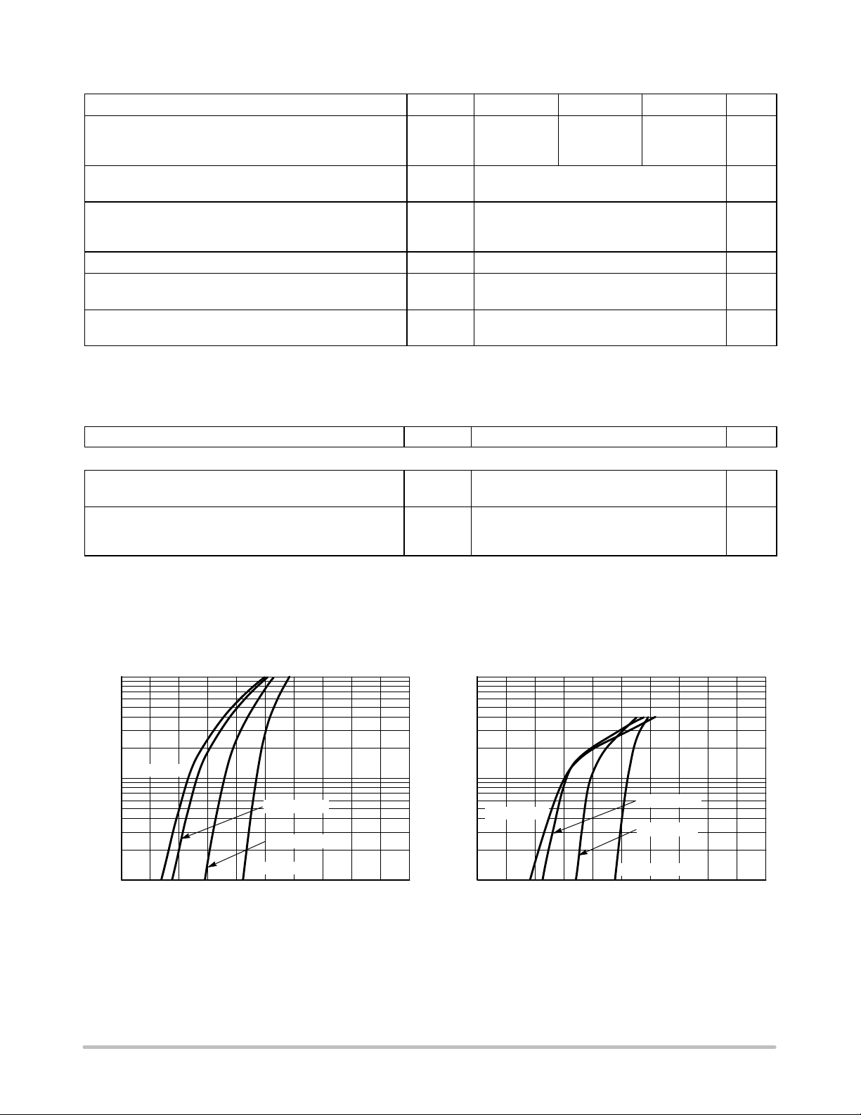
, FORWARD CURRENT (AMPS)
F
I
0.1
0.20.0 0.4 0.6
VF, INSTANTANEOUS FORWARD VOLTAGE (V)
Figure 1. Typical Forward Voltage Figure 2. Maximum Forward Voltage
TYPICAL ELECTRICAL CHARACTERISTICS
10
1
TJ = 100°C
TJ = 25°C
TJ = −65°C
0.8
1.00.30.1 0.5 0.7 0.9
TJ = 125°C
, FORWARD CURRENT (AMPS)
F
I
0.1
VF, MAXIMUM INSTANTANEOUS FORWARD VOLTAGE (V)
TJ = 100°C
TJ = 25°C
TJ = −65°C
0.20.0 0.4 0.6
0.30.1 0.5 0.7 0.9 1.0
0.8
http://onsemi.com
2

MBRS320T3, MBRS330T3, MBRS340T3
TYPICAL ELECTRICAL CHARACTERISTICS (continued)
1.E−01
1.E−02
1.E−03
1.E−04
1.E−05
, REVERSE CURRENT (AMPS)
R
I
1.E−06
TJ = 125°C
TJ = 100°C
TJ = 25°C
0202510 30
515 515
VR, REVERSE VOLTAGE (V)
Figure 3. Typical Reverse Current Figure 4. Maximum Reverse Current
5
4.5
4
3.5
3
2.5
2
1.5
1
0.5
0
, AVERAGE FORWARD CURRENT (AMPS)
O
I
dc
SQUARE WAVE
TL, LEAD TEMPERATURE (°C)
Figure 5. Current Derating Figure 6. Forward Power Dissipation
Freq = 20 kHz
R
= 11°C/W
q
JL
130 140
35 40
15090 100 110 120
1.E−01
1.E−02
1.E−03
1.E−04
1.E−05
, MAXIMUM REVERSE CURRENT (AMPS)
1.E−06
R
I
TJ = 125°C
TJ = 100°C
TJ = 25°C
0202510 30
VR, REVERSE VOLTAGE (V)
2
1.8
1.6
1.4
1.2
1
0.8
0.6
0.4
0.2
, AVERAGE POWER DISSIPATION (W)
0
FO
P
IPK/IO = 5
IO, AVERAGE FORWARD CURRENT (A)
IPK/IO = p
SQUARE
WAVE
3.52.51.50.5
40123
35 40
dc
4.5 5
700
TYPICAL CAPACITANCE AT 0 V = 658 pF
600
500
400
300
200
C, CAPACITANCE (pF)
100
0
4812
VR, REVERSE VOLTAGE (V)
Figure 7. Typical Capacitance
http://onsemi.com
3
TJ = 25°C
28 32 40
360162024
MBRS320T3, MBRS330T3, MBRS340T3
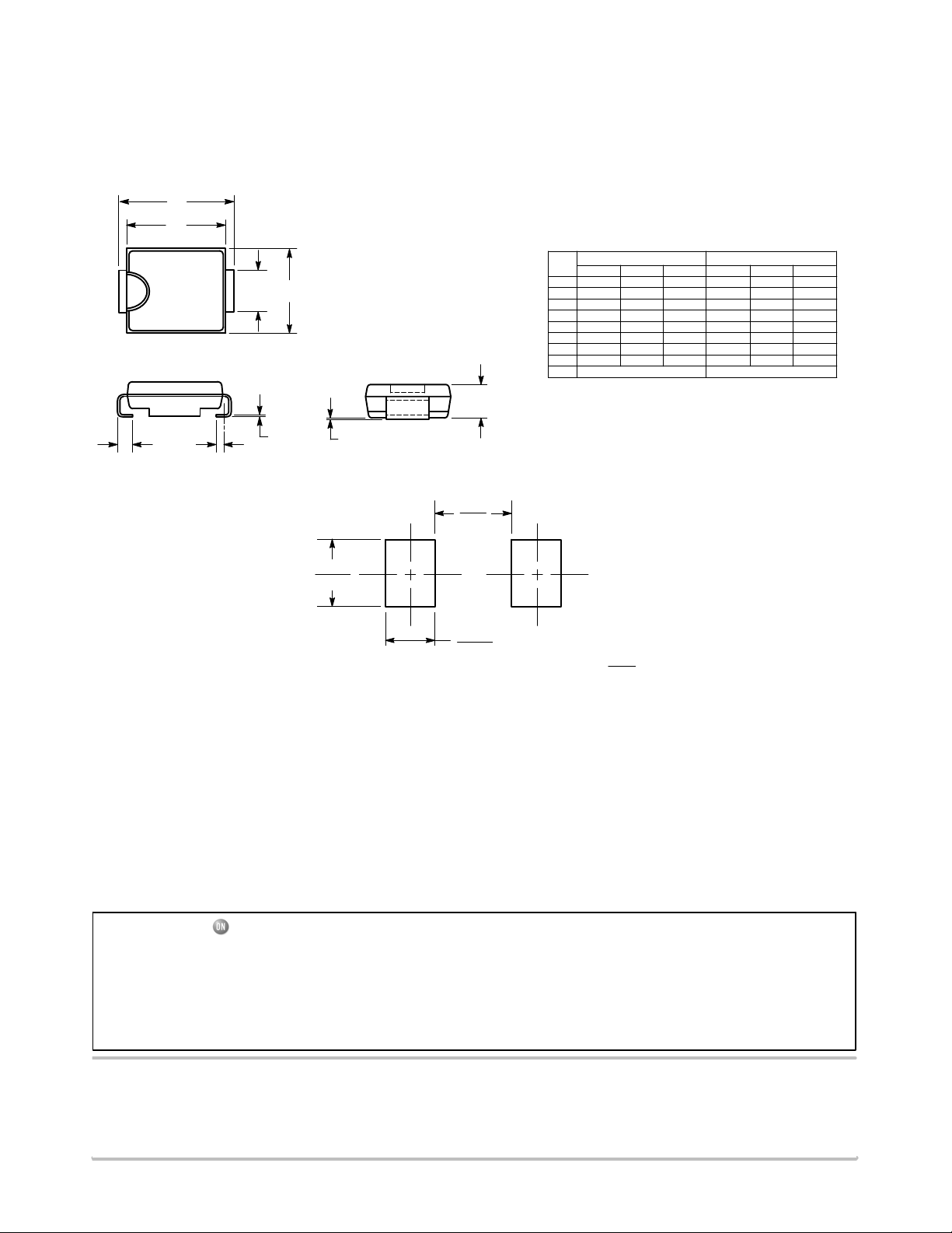
PACKAGE DIMENSIONS
SMC
CASE 403−03
ISSUE E
H
E
E
bD
NOTES:
1. DIMENSIONING AND TOLERANCING PER ANSI Y14.5M, 1982.
2. CONTROLLING DIMENSION: INCH.
3. D DIMENSION SHALL BE MEASURED WITHIN DIMENSION P.
4. 403-01 THRU -02 OBSOLETE, NEW STANDARD 403-03.
DIMAMIN NOM MAX MIN
A1 0.05 0.10 0.15 0.002
b 2.92 3.00 3.07 0.115
c 0.15 0.23 0.30 0.006
D 5.59 5.84 6.10 0.220
E 6.60 6.86 7.11 0.260
H
E
L 0.76 1.02 1.27 0.030
L1
MILLIMETERS
1.90 2.13 2.41 0.075
7.75 7.94 8.13 0.305 0.313 0.320
0.51 REF
INCHES
NOM MAX
0.084 0.095
0.004 0.006
0.118 0.121
0.009 0.012
0.230 0.240
0.270 0.280
0.040 0.050
0.020 REF
A
c
L1L
A1
SOLDERING FOOTPRINT*
4.343
0.171
3.810
0.150
2.794
0.110
SCALE 4:1
ǒ
inches
mm
Ǔ
*For additional information on our Pb−Free strategy and soldering
details, please download the ON Semiconductor Soldering and
Mounting Techniques Reference Manual, SOLDERRM/D.
ON Semiconductor and are registered trademarks of Semiconductor Components Industries, LLC (SCILLC). SCILLC reserves the right to make changes without further notice
to any products herein. SCILLC makes no warranty, representation or guarantee regarding the suitability of its products for any particular purpose, nor does SCILLC assume any liability
arising out of the application or use of any product or circuit, and specifically disclaims any and all liability, including without limitation special, consequential or incidental damages.
“Typical” parameters which may be provided in SCILLC data sheets and/or specifications can and do vary in different applications and actual performance may vary over time. All
operating parameters, including “Typicals” must be validated for each customer application by customer’s technical experts. SCILLC does not convey any license under its patent rights
nor the rights of others. SCILLC products are not designed, intended, or authorized for use as components in systems intended for surgical implant into the body, or other applications
intended to support or sustain life, or for any other application in which the failure of the SCILLC product could create a situation where personal injury or death may occur. Should
Buyer purchase or use SCILLC products for any such unintended or unauthorized application, Buyer shall indemnify and hold SCILLC and its officers, employees, subsidiaries, affiliates,
and distributors harmless against all claims, costs, damages, and expenses, and reasonable attorney fees arising out of, directly or indirectly, any claim of personal injury or death
associated with such unintended or unauthorized use, even if such claim alleges that SCILLC was negligent regarding the design or manufacture of the part. SCILLC is an Equal
Opportunity/Affirmative Action Employer. This literature is subject to all applicable copyright laws and is not for resale in any manner.
PUBLICATION ORDERING INFORMATION
LITERATURE FULFILLMENT:
Literature Distribution Center for ON Semiconductor
P.O. Box 5163, Denver, Colorado 80217 USA
Phone: 303−675−2175 or 800−344−3860 Toll Free USA/Canada
Fax: 303−675−2176 or 800−344−3867 Toll Free USA/Canada
Email: orderlit@onsemi.com
N. American Technical Support: 800−282−9855 Toll Free
USA/Canada
Europe, Middle East and Africa Technical Support:
Phone: 421 33 790 2910
Japan Customer Focus Center
Phone: 81−3−5773−3850
ON Semiconductor Website: www.onsemi.com
Order Literature: http://www.onsemi.com/orderlit
For additional information, please contact your local
Sales Representative
http://onsemi.com
4
MBRS340T3/D
 Loading...