

MBRD1035CTL
SWITCHMODEt
Schottky Power Rectifier
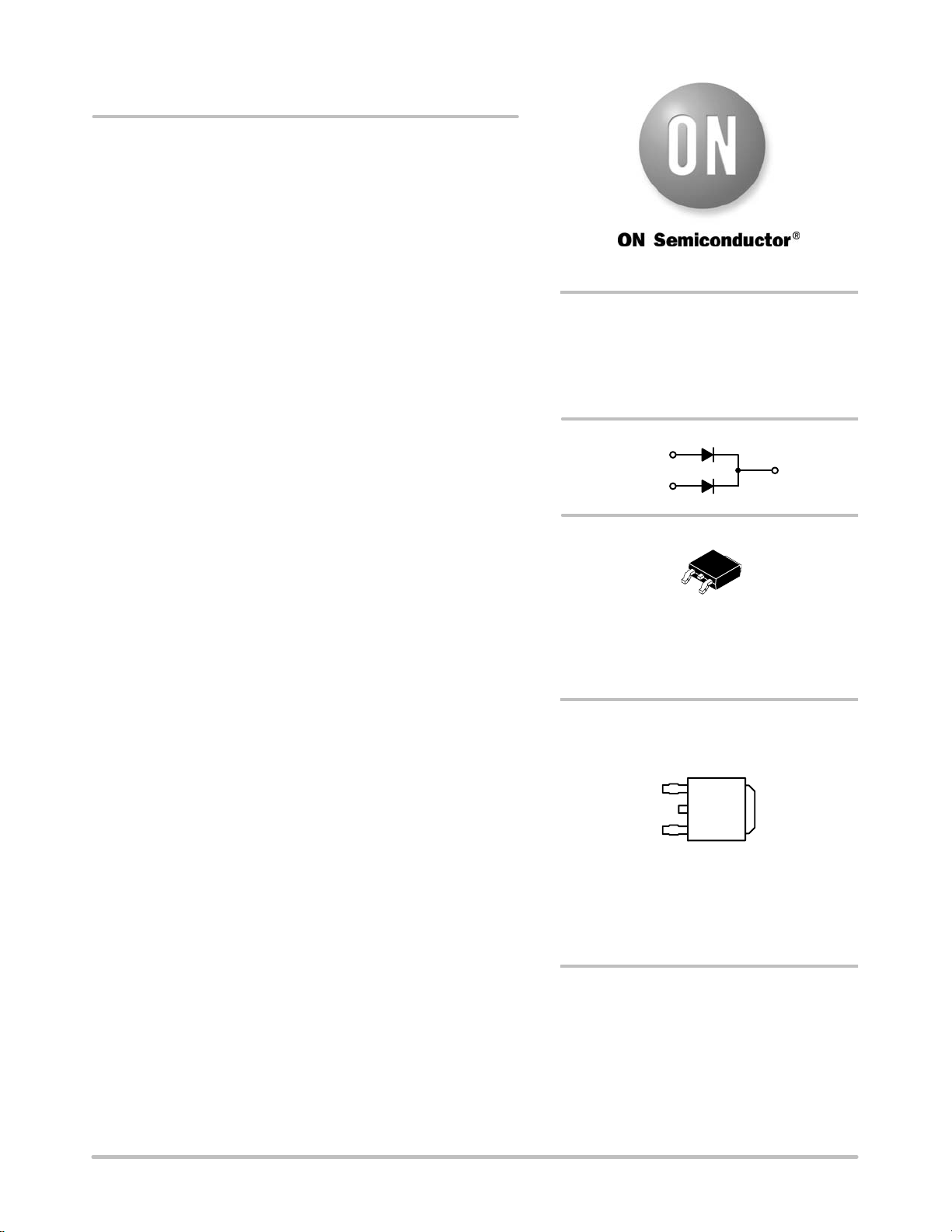
DPAK Power Surface Mount Package
The MBRD1035CTL employs the Schottky Barrier principle in a
large area metal−to−silicon power diode. State of the art geometry
features epitaxial construction with oxide passivation and metal
overlay contact. Ideally suited for low voltage, high frequency
switching power supplies, free wheeling diode and polarity protection
diodes.
Features
• Highly Stable Oxide Passivated Junction
• Guardring for Stress Protection
• Matched Dual Die Construction −
May be Paralleled for High Current Output
• High dv/dt Capability
• Short Heat Sink Tap Manufactured − Not Sheared
• Very Low Forward Voltage Drop
• Epoxy Meets UL 94 V−0 @ 0.125 in
• Pb−Free Packages are Available
Mechanical Characteristics:
• Case: Epoxy, Molded
• Weight: 0.4 Gram (Approximately)
• Finish: All External Surfaces Corrosion Resistant and Terminal
Leads are Readily Solderable
• Lead and Mounting Surface Temperature for Soldering Purposes:
260°C Max. for 10 Seconds
http://onsemi.com
SCHOTTKY BARRIER
RECTIFIER
10 AMPERES
35 VOLTS
1
3
2
1
3
DPAK
CASE 369C
MARKING DIAGRAM
4
4
© Semiconductor Components Industries, LLC, 2006
January, 2006 − Rev. 6
YWW
B10
35CLG
Y = Year
WW = Work Week
B1035CL = Device Code
G = Pb−Free Package
ORDERING INFORMATION
See detailed ordering and shipping information in the package
dimensions section on page 2 of this data sheet.
1 Publication Order Number:
MBRD1035CTL/D

MBRD1035CTL
MAXIMUM RATINGS
Rating Symbol Value Unit
Peak Repetitive Reverse Voltage
Working Peak Reverse Voltage
DC Blocking Voltage
Average Rectified Forward Current Per Leg
(At Rated VR, TC = 115°C) Per Package
Peak Repetitive Forward Current Per Leg
(At Rated VR, Square Wave, 20 kHz, TC = 115°C)
Non−Repetitive Peak Surge Current Per Package
(Surge applied at rated load conditions, halfwave, single phase, 60 Hz)
Storage / Operating Case Temperature T
Operating Junction Temperature (Note 1) T
Voltage Rate of Change (Rated VR, TJ = 25°C) dv/dt 10,000
Maximum ratings are those values beyond which device damage can occur. Maximum ratings applied to the device are individual stress limit
values (not normal operating conditions) and are not valid simultaneously. If these limits are exceeded, device functional operation is not implied,
damage may occur and reliability may be affected.
1. The heat generated must be less than the thermal conductivity from Junction−to−Ambient: dPD/dTJ < 1/R
THERMAL CHARACTERISTICS
Thermal Resistance, Junction−to−Case Per Leg
Thermal Resistance, Junction−to−Ambient (Note 2) Per Leg
V
V
I
I
stg,
R
R
RRM
RWM
V
R
I
O
FRM
FSM
J
q
JC
q
JA
35 V
5.0
A
10
10 A
50 A
T
c
−55 to +150 °C
−55 to +150 °C
V/ms
.
q
JA
3.0 °C/W
137 °C/W
ELECTRICAL CHARACTERISTICS
Maximum Instantaneous Forward Voltage (Note 3)
(See Figure 2) Per Leg
IF = 5 Amps, TJ = 25°C
IF = 5 Amps, TJ = 100°C
IF = 10 Amps, TJ = 25°C
IF = 10 Amps, TJ = 100°C
Maximum Instantaneous Reverse Current (Note 3)
(See Figure 4) Per Leg
(VR = 35 V, TJ = 25°C)
(VR = 35 V, TJ = 100°C)
(VR = 17.5 V, TJ = 25°C)
(VR = 17.5 V, TJ = 100°C)
2. Rating applies when using minimum pad size, FR4 PC Board
3. Pulse Test: Pulse Width ≤ 250 ms, Duty Cycle ≤ 2.0%
V
F
V
0.47
0.41
0.56
0.55
I
R
mA
2.0
30
0.20
5.0
ORDERING INFORMATION
Device Package Shipping
MBRD1035CTL DPAK 75 Units / Rail
MBRD1035CTLG DPAK
75 Units / Rail
(Pb−Free)
MBRD1035CTLT4 DPAK 2500 Units / Tape & Reel
MBRD1035CTLT4G DPAK
2500 Units / Tape & Reel
(Pb−Free)
†For information on tape and reel specifications, including part orientation and tape sizes, please refer to our Tape and Reel Packaging
Specifications Brochure, BRD8011/D.
†
http://onsemi.com
2
 Loading...