

MBR2030CTL
SWITCHMODE™ Dual
Schottky Power Rectifier
Features and Benefits
• Highly Stable Oxide Passivated Junction
• Very Low Forward Voltage Drop (0.4 Max @ 10 A, T
• High Junction Temperature
• High dv/dt Capability
• Excellent Ability to Withstand Reverse Avalanche Energy Transients
• Low Power Loss / High Efficiency
• High Surge Capacity
• 175°C Operating Junction Temperature
• 20 A Total (10 A Per Diode Leg)
• Pb−Free Package is Available*
Applications
• Power Supply − Output Rectification
• Power Management − ORING
• Instrumentation
= 150°C)
C
http://onsemi.com
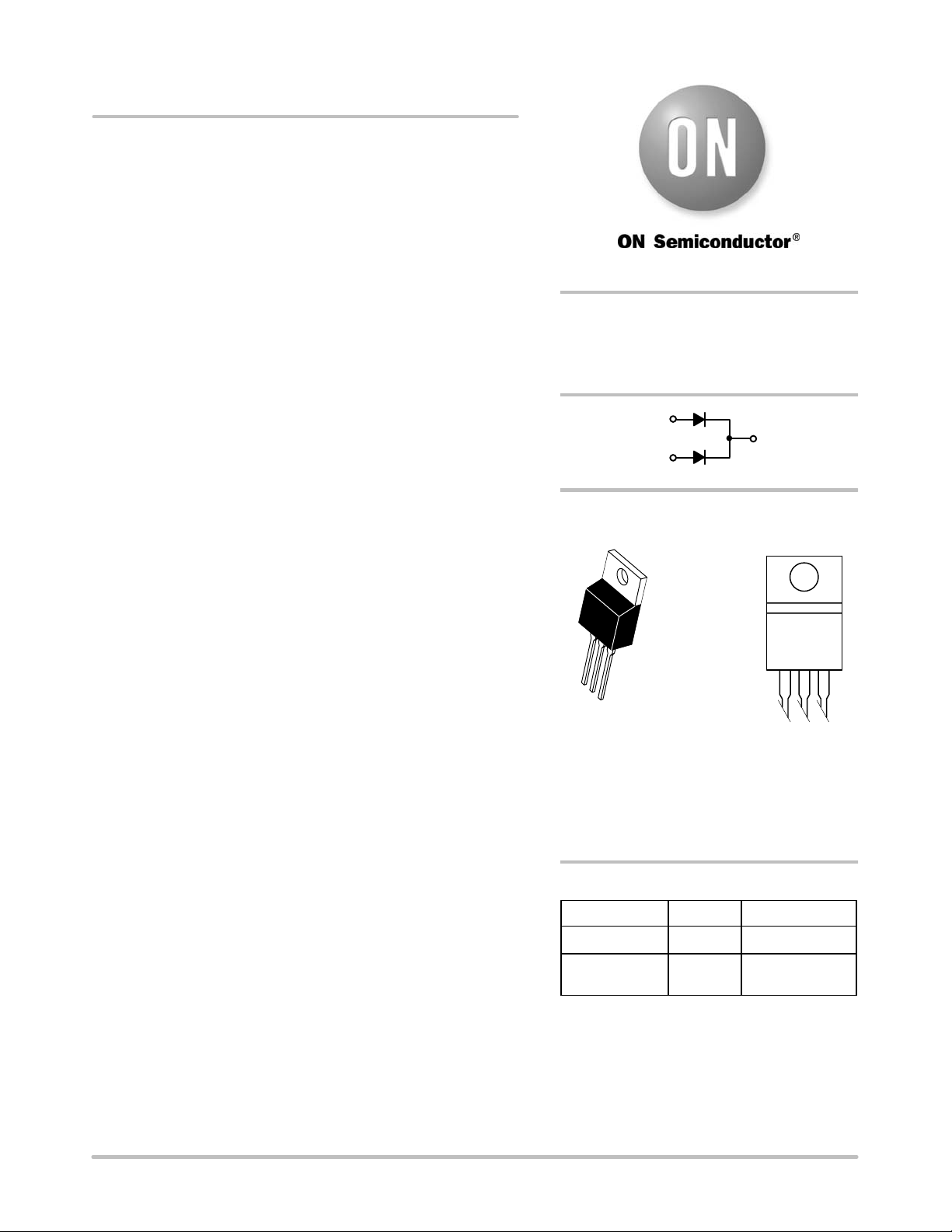
SCHOTTKY BARRIER
RECTIFIER
20 AMPERES, 30 VOLTS
1
2, 4
3
MARKING
DIAGRAM
4
Mechanical Characteristics
• Case: Epoxy, Molded
• Epoxy Meets UL 94 V−0 @ 0.125 in
• Weight: 1.9 Grams (Approximately)
• Finish: All External Surfaces Corrosion Resistant and Terminal
Leads are Readily Solderable
• Lead Temperature for Soldering Purposes: 260°C Max. for 10 Sec
• ESD Rating: Human Body Model 3B
Machine Model C
TO−220AB
CASE 221A
PLASTIC
1
2
3
A = Assembly Location
Y = Year
WW = Work Week
B2030L = Device Code
G = Pb−Free Package
AKA = Diode Polarity
ORDERING INFORMATION
Device Package Shipping
MBR2030CTL TO−220 50 Units/Rail
MBR2030CTLG TO−220
(Pb−Free)
AYWW
B2030LG
AKA
50 Units/Rail
*For additional information on our Pb−Free strategy and soldering details, please
download the ON Semiconductor Soldering and Mounting Techniques
Reference Manual, SOLDERRM/D.
© Semiconductor Components Industries, LLC, 2006
July, 2006 − Rev. 4
1 Publication Order Number:
MBR2030CTL/D
MBR2030CTL
MAXIMUM RATINGS (Per Leg)
Rating
Peak Repetitive Reverse Voltage
Working Peak Reverse Voltage
DC Blocking Voltage
Average Rectified Forward Current
(TC = 167_C) Per Diode
Per Device
Nonrepetitive Peak Surge Current
(Surge applied at rated load conditions halfwave, single phase, 60 Hz)
Peak Repetitive Forward Current
(Square Wave, 20 kHz, TC = 166°C)
Peak Repetitive Reverse Surge Current (2.0 ms, 1.0 kHz)
Operating Junction Temperature (Note 1) T
Storage Temperature T
Voltage Rate of Change (Rated VR) dv/dt 1000
Stresses exceeding Maximum Ratings may damage the device. Maximum Ratings are stress ratings only. Functional operation above the
Recommended Operating Conditions is not implied. Extended exposure to stresses above the Recommended Operating Conditions may affect
device reliability.
THERMAL CHARACTERISTICS (Per Leg)
Rating Symbol Value Unit
Maximum Thermal Resistance, Junction−to−Case (Min. Pad)
Maximum Thermal Resistance, Junction−to−Ambient (Min. Pad)
Symbol Value Unit
V
V
I
F(AV)
RRM
RWM
V
R
30 V
A
10
20
I
FSM
I
FRM
I
RRM
J
stg
150 A
10 A
1.0 A
*65 to +175 °C
*65 to +175 °C
V/ms
R
q
JC
R
q
JA
2.0 °C/W
60 °C/W
ELECTRICAL CHARACTERISTICS (Per Leg)
Characteristic Symbol Min Typ Max Unit
Maximum Instantaneous Forward Voltage (Note 2)
(iF = 10 Amps, TJ= 25°C)
(iF = 10 Amps, TJ = 150°C)
(iF = 20 Amps, TJ = 25°C)
(iF = 20 Amps, TJ = 150°C)
Maximum Instantaneous Reverse Current (Note 2)
(Rated dc Voltage, TJ = 25°C)
(Rated dc Voltage, TJ = 100°C)
(Rated dc Voltage, TJ = 125°C)
1. The heat generated must be less than the thermal conductivity from Junction−to−Ambient: dPD/dTJ < 1/R
2. Pulse Test: Pulse Width = 5.0 ms, Duty Cycle ≤ 10%.
v
F
i
R
0.45
0.32
0.51
0.41
0.52
0.40
0.58
0.48
−
−
−
−
mA
−
V
0.11
−
−
.
q
JA
10
5.0
40
−
75
http://onsemi.com
2

MBR2030CTL
100
T
= 175°C
J
10
150°C
100°C
1.0
0.1
F
i , INSTANTANEOUS FORWARD CURRENT (AMPS)
0.2 0.4
0.1 0.3 0.5 0.7 0.9 1.10.0
v
INSTANTANEOUS FORWARD VOLTAGE (VOLTS)
F,
25°C
0.6 0.8
Figure 1. Typical Forward Voltage
10000
4000
2000
1000
400
200
100
40
20
10
4
2
1
0.4
R
I , REVERSE CURRENT (mA)
0.2
0.1
0.04
0.02
0.01
01510 25 30
520
TJ = 150°C
TJ = 100°C
TJ = 25°C
VR REVERSE VOLTAGE (VOLTS)
1.0
100
10
1.0
0.1
F
i , INSTANTANEOUS FORWARD CURRENT (AMPS)
20
18
16
14
12
10
8.0
6.0
4.0
2.0
F (AV)
I , AVERAGE FORWARD CURRENT (AMPS)
T
= 175°C
J
150°C
0.2 0.4
0.1 0.3 0.5 0.7 0.9 1.10.0
v
INSTANTANEOUS FORWARD VOLTAGE (VOLTS)
F,
Figure 2. Maximum Forward Voltage
dc
SQUARE WAVE
0
145 155 160
140
100°C
25°C
0.6 0.8
150
TC, CASE TEMPERATURE (C°)
165
170 175
1.0
180
Figure 3. Typical Reverse Current
20
18
RATED VOLTAGE APPLIED
16
14
12
10
dc
SQUARE WAVE
8.0
6.0
4.0
2.0
F (AV)
0
I , AVERAGE FORWARD CURRENT (AMPS)
05025 75
100 125 150 175
TA, AMBIENT TEMPERATURE (°C)
Figure 5. Current Derating, Ambient Per Leg
R
= 16° C/Wdc
q
JA
R
= 60° C/W
q
JA
(NO HEATSINK)
http://onsemi.com
Figure 4. Current Derating, Case Per Leg
30
28
TJ = 175°C
26
24
22
SQUARE WAVE
20
18
16
14
12
dc
10
8
6
4
2
0
04 12816
210614182226
I
, AVERAGE FORWARD CURRENT (AMPS)
F (AV)
P , AVERAGE FORWARD POWER DISSIPATION (WATTS)
F(AV)
20 24 28 30
Figure 6. Forward Power Dissipation
3

10K
MBR2030CTL
5000
3000
2000
1000
500
C, CAPACITANCE (pF)
300
200
100
0.5 2
1
3 5 10 20 30 50
VR, REVERSE VOLTAGE (VOLTS)
Figure 7. Typical Capacitance
TJ = 25°C
f = 1 MHz
http://onsemi.com
4

MBR2030CTL
PACKAGE DIMENSIONS
TO−220AB
CASE 221A−09
ISSUE AA
SEATING
−T−
PLANE
B
4
Q
123
F
T
A
U
C
S
H
K
Z
L
V
R
J
G
D
N
NOTES:
1. DIMENSIONING AND TOLERANCING PER ANSI
Y14.5M, 1982.
2. CONTROLLING DIMENSION: INCH.
3. DIMENSION Z DEFINES A ZONE WHERE ALL
BODY AND LEAD IRREGULARITIES ARE
ALLOWED.
DIM MIN MAX MIN MAX
A 0.570 0.620 14.48 15.75
B 0.380 0.405 9.66 10.28
C 0.160 0.190 4.07 4.82
D 0.025 0.035 0.64 0.88
F 0.142 0.147 3.61 3.73
G 0.095 0.105 2.42 2.66
H 0.110 0.155 2.80 3.93
J 0.018 0.025 0.46 0.64
K 0.500 0.562 12.70 14.27
L 0.045 0.060 1.15 1.52
N 0.190 0.210 4.83 5.33
Q 0.100 0.120 2.54 3.04
R 0.080 0.110 2.04 2.79
S 0.045 0.055 1.15 1.39
T 0.235 0.255 5.97 6.47
U 0.000 0.050 0.00 1.27
V 0.045 −−− 1.15 −−−
Z −−− 0.080 −−− 2.04
STYLE 6:
PIN 1. ANODE
2. CATHODE
3. ANODE
4. CATHODE
MILLIMETERSINCHES
SWITCHMODE is a trademark of Semiconductor Components Industries, LLC.
ON Semiconductor and are registered trademarks of Semiconductor Components Industries, LLC (SCILLC). SCILLC reserves the right to make changes without further notice
to any products herein. SCILLC makes no warranty, representation or guarantee regarding the suitability of its products for any particular purpose, nor does SCILLC assume any liability
arising out of the application or use of any product or circuit, and specifically disclaims any and all liability, including without limitation special, consequential or incidental damages.
“Typical” parameters which may be provided in SCILLC data sheets and/or specifications can and do vary in different applications and actual performance may vary over time. All
operating parameters, including “Typicals” must be validated for each customer application by customer’s technical experts. SCILLC does not convey any license under its patent rights
nor the rights of others. SCILLC products are not designed, intended, or authorized for use as components in systems intended for surgical implant into the body, or other applications
intended to support or sustain life, or for any other application in which the failure of the SCILLC product could create a situation where personal injury or death may occur. Should
Buyer purchase or use SCILLC products for any such unintended or unauthorized application, Buyer shall indemnify and hold SCILLC and its officers, employees, subsidiaries, affiliates,
and distributors harmless against all claims, costs, damages, and expenses, and reasonable attorney fees arising out of, directly or indirectly, any claim of personal injury or death
associated with such unintended or unauthorized use, even if such claim alleges that SCILLC was negligent regarding the design or manufacture of the part. SCILLC is an Equal
Opportunity/Affirmative Action Employer. This literature is subject to all applicable copyright laws and is not for resale in any manner.
PUBLICATION ORDERING INFORMATION
LITERATURE FULFILLMENT:
Literature Distribution Center for ON Semiconductor
P.O. Box 5163, Denver, Colorado 80217 USA
Phone: 303−675−2175 or 800−344−3860 Toll Free USA/Canada
Fax: 303−675−2176 or 800−344−3867 Toll Free USA/Canada
Email: orderlit@onsemi.com
N. American Technical Support: 800−282−9855 Toll Free
USA/Canada
Europe, Middle East and Africa Technical Support:
Phone: 421 33 790 2910
Japan Customer Focus Center
Phone: 81−3−5773−3850
http://onsemi.com
ON Semiconductor Website: www.onsemi.com
Order Literature: http://www.onsemi.com/orderlit
For additional information, please contact your local
Sales Representative
MBR2030CTL/D
5
 Loading...