

ON Semiconductor MBR120ESFT1 Technical data
MBR120ESFT1
l
l
)
l
l
s
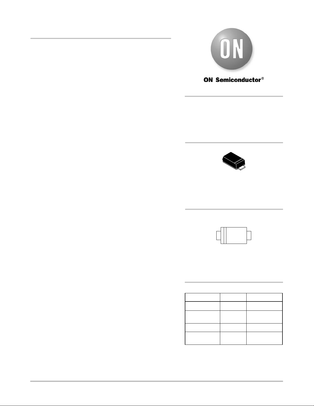
Surface Mount
Schottky Power Rectifier
Plastic SOD−123 Package
This device uses the Schottky Barrier principle with a large area
metal−to−silicon power diode. Ideally suited for low voltage, high
frequency rectification or as free wheeling and polarity protection
diodes in surface mount applications where compact size and weight
are critical to the system. This package also provides an easy to work
with alternative to leadless 34 package style. Because of its small size,
it is ideal for use in portable and battery powered products such as
cellular and cordless phones, chargers, notebook computers, printers,
PDAs and PCMCIA cards. Typical applications are AC−DC and
DC−DC converters, reverse battery protection, and “Oring” of
multiple supply voltages and any other application where performance
and size are critical.
Features
• Guardring for Stress Protection
• Low Leakage
• 150°C Operating Junction Temperature
• Epoxy Meets UL 94 V−0 @ 0.125 in
• Package Designed for Optimal Automated Board Assembly
• ESD Ratings: Machine Model, C
ESD Ratings: Human Body Model, 3B
• Pb−Free Packages are Available
Mechanical Characteristics
• Reel Options: MBR120ESFT1 = 3,000 per 7″ reel/8 mm tape
MBR120ESFT3 = 10,000 per 13″ reel/8 mm tape
• Device Marking: L2E
• Polarity Designator: Cathode Band
• Weight: 11.7 mg (approximately)
• Case: Epoxy, Molded
• Finish: All External Surfaces Corrosion Resistant and Terminal
Leads are Readily Solderable
• Lead and Mounting Surface Temperature for Soldering Purposes:
260°C Max. for 10 Seconds
http://onsemi.com
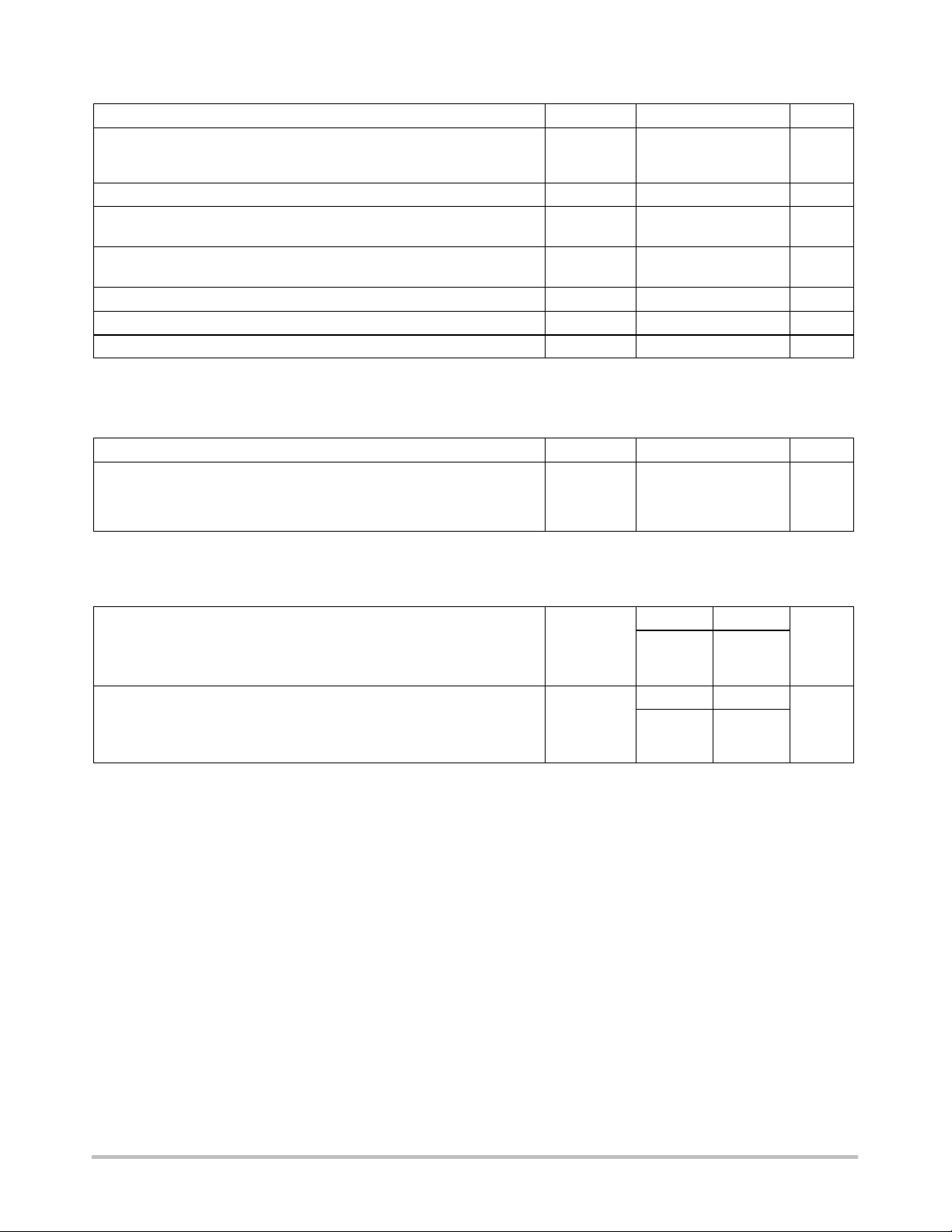
SCHOTTKY BARRIER
RECTIFIER
1.0 AMPERES
20 VOLTS
SOD−123FL
CASE 498
PLASTIC
MARKING DIAGRAM
M
L2E
G
G
L2E = Specific Device Code
M = Date Code
G = Pb−Free Package
(Note: Microdot may be in either location
ORDERING INFORMATION
Device Package Shipping
MBR120ESFT1 SOD−123FL
MBR120ESFT1G SOD−123FL
(Pb−Free)
MBR120ESFT3 SOD−123FL 10000/Tape & Ree
MBR120ESFT3G SOD−123FL
(Pb−Free)
†For information on tape and reel specifications,
including part orientation and tape sizes, please
refer to our Tape and Reel Packaging Specification
Brochure, BRD8011/D.
3000/Tape & Ree
3000/Tape & Ree
10000/Tape & Ree
†
© Semiconductor Components Industries, LLC, 2005
July, 2005 − Rev. 2
1 Publication Order Number:
MBR120ESFT1/D
MBR120ESFT1
MAXIMUM RATINGS
Rating Symbol Value Unit
Peak Repetitive Reverse Voltage
Working Peak Reverse Voltage
DC Blocking Voltage
Average Rectified Forward Current (At Rated VR, TL = 140°C) I
Peak Repetitive Forward Current
(At Rated V
, Square Wave, 20 kHz, TL = 125°C)
R
Non−Repetitive Peak Surge Current
(Non−Repetitive peak surge current, halfwave, single phase, 60 Hz)
Storage Temperature T
Operating Junction Temperature T
Voltage Rate of Change (Rated VR, TJ = 25°C) dv/dt 10,000
Maximum ratings are those values beyond which device damage can occur. Maximum ratings applied to the device are individual stress limit
values (not normal operating conditions) and are not valid simultaneously. If these limits are exceeded, device functional operation is not implied,
damage may occur and reliability may be affected.
THERMAL CHARACTERISTICS
Rating Symbol Value Unit
Thermal Resistance − Junction−to−Lead (Note 1)
Thermal Resistance − Junction−to−Lead (Note 2)
Thermal Resistance − Junction−to−Ambient (Note 1)
Thermal Resistance − Junction−to−Ambient (Note 2)
1. Mounted with minimum recommended pad size, PC Board FR4.
2. Mounted with 1 in. copper pad (Cu area 700 mm2).
V
V
RRM
RWM
V
I
FRM
I
FSM
R
R
R
R
stg
20 V
R
O
1.0 A
2.0 A
40 A
−65 to 150 °C
J
−65 to 150 °C
V/ms
tjl
tjl
tja
tja
26
21
325
82
°C/W
ELECTRICAL CHARACTERISTICS
Maximum Instantaneous Forward Voltage (Note 3), See Figure 2
(IF = 0.1 A)
(IF = 1.0 A)
(IF = 2.0 A)
Maximum Instantaneous Reverse Current (Note 3), See Figure 4
(VR = 20 V)
(VR = 10 V)
(VR = 5.0 V)
3. Pulse Test: Pulse Width ≤ 250 ms, Duty Cycle ≤ 2%.
V
F
I
R
TJ = 25°C TJ = 100°C
0.455
0.530
0.595
0.360
0.455
0.540
TJ = 25°C TJ = 100°C mA
10
1.0
0.5
1600
500
300
V
http://onsemi.com
2
 Loading...