

Page 1

EVBUM2775/D
Attention: The SECO−1kW−MCTRL−GEVB is powered by AC Mains, and exposed to high voltage. Only trained
Compact Intelligent Power
Module (IPM) Motor Control
Development Kit (MDK)
1 kW
This User Guides refer to revision 0.4 of the
SECO−1KW−MCTRL−GEVK evaluation board.
Description
This user guide provides practical guidelines for compact
Intelligent Power Module (IPM) evaluation board with
interleaved power factor Correction (PFC)
SECO−1KW−MCTRL−GEVB including its main features
and key data. The board is fully compatible with the
Universal Controller Board (UCB), based on the Xilinx
Zynq−7000 SoC, which embeds FPGA logic and two ARM
Cortex−A9 processors. As such, the system is fit for
high−end control strategies and enables operation of a
variety of motor technologies (AC induction motor, PMSM,
BLDC, etc.). The board was developed to support customers
during their first steps designing application with IPM and
PFC. The design was tested as described in this document
but not qualified regarding safety requirements or
manufacturing and operation over the whole operating
temperature range or lifetime. The board is intended for
functional testing under laboratory conditions and by
trained specialists only.
Collateral
• SECO−1KW−MCTRL−GEVB
• Universal Controller Board (UCB)
• NFAQ1060L36T
• NCP1632
• FCPF125N65S3
• NCP1063
• NCS2003
• NCS2250
Features
• 850 W complete motor control solution with AC mains
• Compatible with Universal Controller Board (UCB)
• User−friendly GUI with V/f and FOC control use cases
• Highly integrated power module NFAQ1060L36T
• PFC stage using NCP1632 controller, FCPF125N65S3
• DC/DC converter producing auxiliary power supply
• 3 phase current measurement using 3 x NCS2003
• Over current protection using NCS2250 comparator
www.onsemi.com
EVAL BOARD USER’S MANUAL
supply 230 Vrms ±15 %, EMI filter, 2−channel
interleaved Power Factor Correction (PFC)
FPGA−controller based on Xilinx Zynq− 7000 SoC
for rapid evaluation
containing an inverter power stage for a high voltage
3−phase inverter in a DIP−S3 package
NMOS power transistors and FFSPF1065A diodes
15VDC – non−isolated buck converter using NCP1063
operational amplifier
personnel should manipulate and operate on the system. Ensure that all boards are properly connected before
powering, and that power is off before disconnecting any boards. It is mandatory to read the Safety Precautions
section before manipulating the board. Failure to comply with the described safety precautions may result in
personal injury or death, or equipment damage.
© Semiconductor Components Industries, LLC, 2020
March, 2021 − Rev. 1
1 Publication Order Number:
EVBUM2775/D
Page 2
EVBUM2775/D
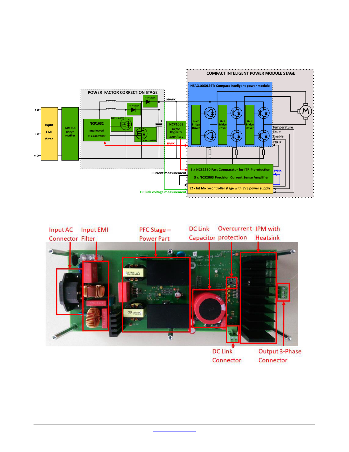
Overview
The block diagram of the whole system is represented in
Figure 1. The picture of the real board is in the Figure 2 and
Figure 3.
Figure 1. Block Diagram of the Evaluation Board
Figure 2. Picture of the Evaluation Board – Top Side
www.onsemi.com
2
Page 3
EVBUM2775/D
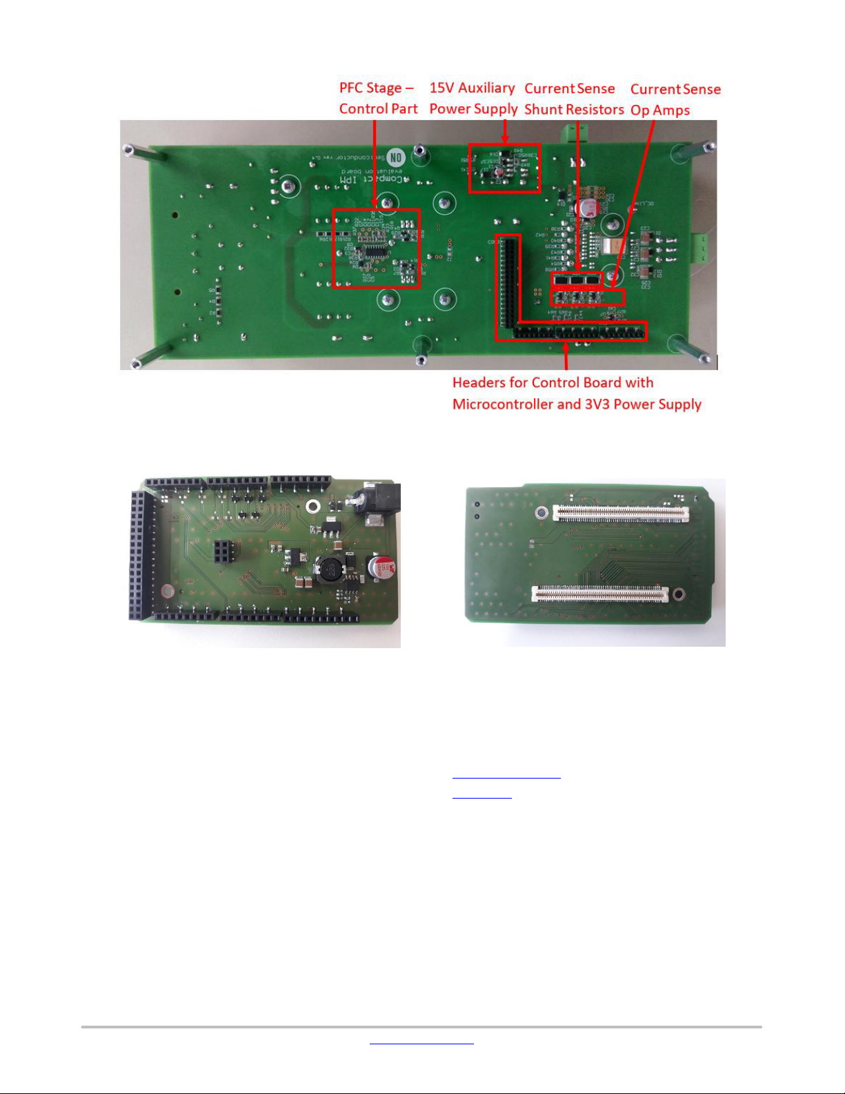
Figure 3. Picture of the Evaluation Board – Bottom Side
(Top Side) (Bottom Side)
Figure 4. Picture of the UCB Adapter
PREREQUISITES
Hardware
• SECO−1 kW−MCTRL−GEVB (includes power board
and adapter for UCB)
• AC power cord one−phase
• Universal Controller Board (UCB) or pin−compatible
controller board
• USB isolator (5 kV optical isolation)
• HF ferrite clamp i.e. WE 7427154
www.onsemi.com
Software
• Downloadable GUI
• Binary file
3
Page 4
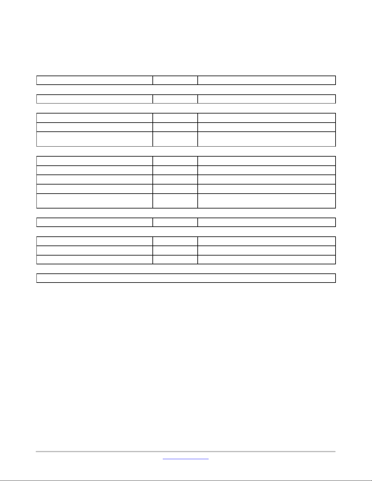
SPECIFICATION
Table 1. EVALUATION BOARD SPECIFICATIONS
Parameters
Values
Conditions/comments
INPUT
Voltage
230 V
15%
OUTPUT
Power
850 W
Input 230 VAC, f
= 16 kHz, T
= 25°C
Current per IPM leg
5 A
T
= 100°C
DC BUS Voltage
390 V
Higher voltage value is created by interleaved PFC with
CURRENT FEEDBACK
Current sensing resistors
39 m
Op Amp power supply
3.3 V
Set Op Amp gain
5
Set output offset
1.65 V
Because of negative current measurement
Overcurrent protection
9 A
Configured by shunt resistors and comparator threshold
AUXILIARY POWER SUPPLY
15 V
4.6 W
Used NCP1063
CONTROL
Board with Microcontroller and 3V3 power supply
Arduino DUE headers
Type of control
V/f, Field Oriented Control (Sensor−less)
Supported type of motors
ACIM, PMSM, BLDC
APPLICATION
White goods (washers), Industrial fans, Industrial automation
The specification and main features can be seen in the
Table 1.
EVBUM2775/D
±
rms
PWM
±
rms
C
A
NCP1632 working as a booster
W
peak
(voltage divider)
www.onsemi.com
4
Page 5
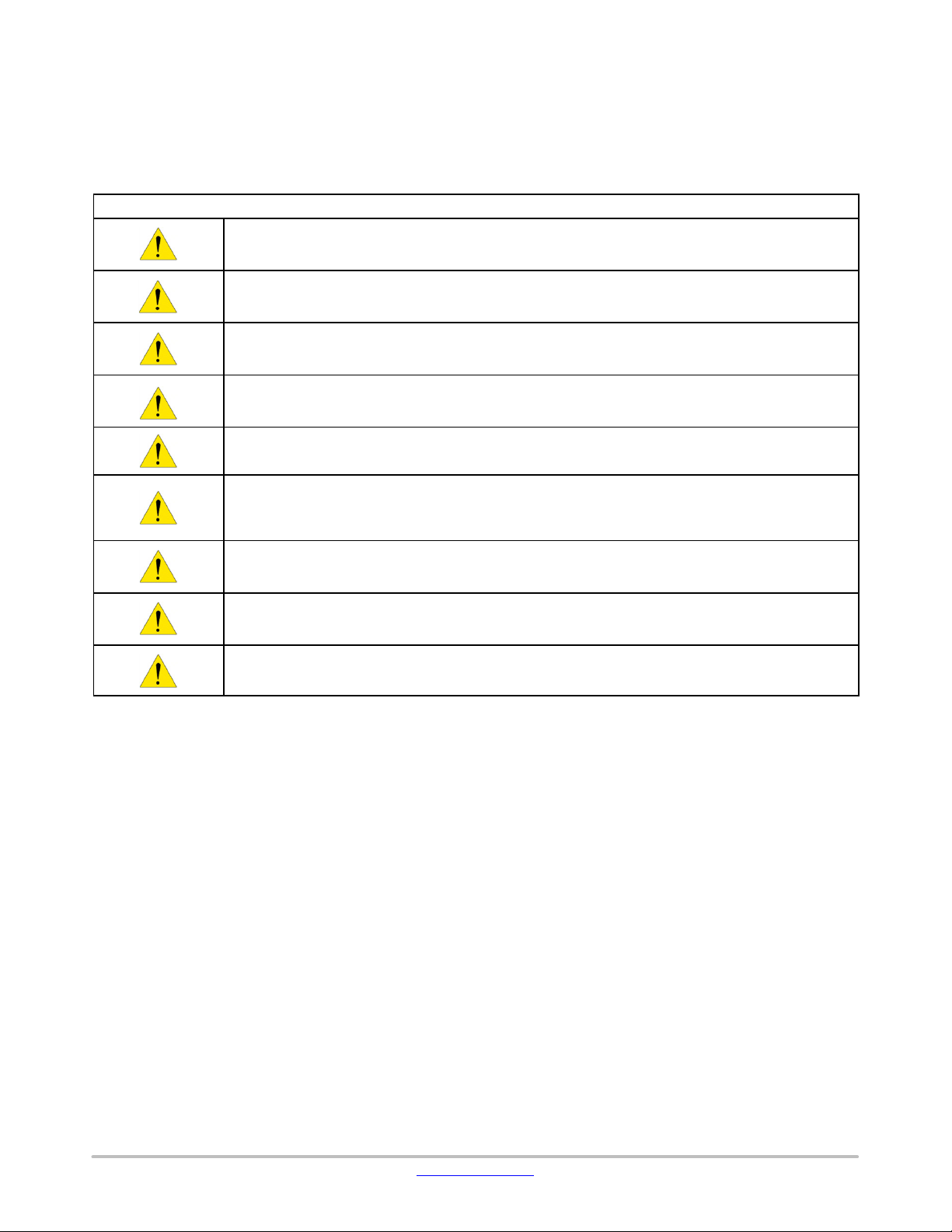
SAFETY PRECAUTIONS
T able 2.
SECO−1KW−MCTRL−GEVB
The ground potential of the system is biased to a negative DC bus voltage potential. When measuring voltage
The ground potential of the system is NOT biased to an earth (PE) potential. When connecting the MCU board
SECO−1KW−MCTRL−GEVB system contains DC bus capacitors which take time to discharge after removal of
Only personnel familiar with the drive and associated machinery should plan or implement the installation,
The surfaces of the drive may become hot, which may cause injury.
SECO−1KW−MCTRL−GEVB system contains parts and assemblies sensitive to Electrostatic Discharge (ESD).
A drive, incorrectly applied or installed, can result in component damage or reduction in product lifetime.
Remove and lock out power from the drive before you disconnect or reconnect wires or perform service. Wait
SECO−1KW−MCTRL−GEVB system is shipped with packing materials that need to be removed prior to
It is mandatory to read the following precautions before
manipulating the SECO−1KW−MCTRL−GEVB.
waveform by oscilloscope, the scope’s ground needs to be isolated. Failure to do so may result in personal
injury or death
via USB to the computer, the appropriate galvanically isolated USB isolator have to be used. The recommended
isolation voltage of USB isolator is 5 kV
the main supply. Before working on the drive system, wait ten minutes for capacitors to discharge to safe voltage levels. Failure to do so may result in personal injury or death.
start−up and subsequent maintenance of the system. Failure to comply may result in personal injury and/or
equipment damage.
Electrostatic control precautions are required when installing, testing, servicing or repairing this assembly.
Component damage may result if ESD control procedures are not followed. If you are not familiar with
electrostatic control procedures, refer to applicable ESD protection handbooks and guidelines.
EVBUM2775/D
Wiring or application errors such as under sizing the motor, supplying an incorrect or inadequate AC supply or
excessive ambient temperatures may result in system malfunction.
ten minutes after removing power to discharge the bus capacitors. Do not attempt to service the drive until the
bus capacitors have discharged to zero. Failure to do so may result in personal injury or death.
installation. Failure to remove all packing materials which are unnecessary for system installation may result in
overheating or abnormal operating condition.
www.onsemi.com
5
Page 6
EVBUM2775/D
SCHEMATICS AND LAYOUT
To meet customer requirements and make the evaluation
board a basis for development, all necessary technical data
like schematics, layout and components are included in this
chapter. Also simple measurements were done to show the
functionality of individual stages.
4 A
L_IN
N_IN
PE
AC_IN
i
PHASE_EMI_IN
R1
2R2
PE
AC_IN
F1
i
10 A
PHASE _EMI_0 1
R3
NEUTRAL_EMI_IN
AC_IN
i
R2
680k
R4
680k
R5
680k
i
NEUTRAL_IN
PE
i
L5
C16
1 mF
1−1
2−1
2 x 2.2 mH
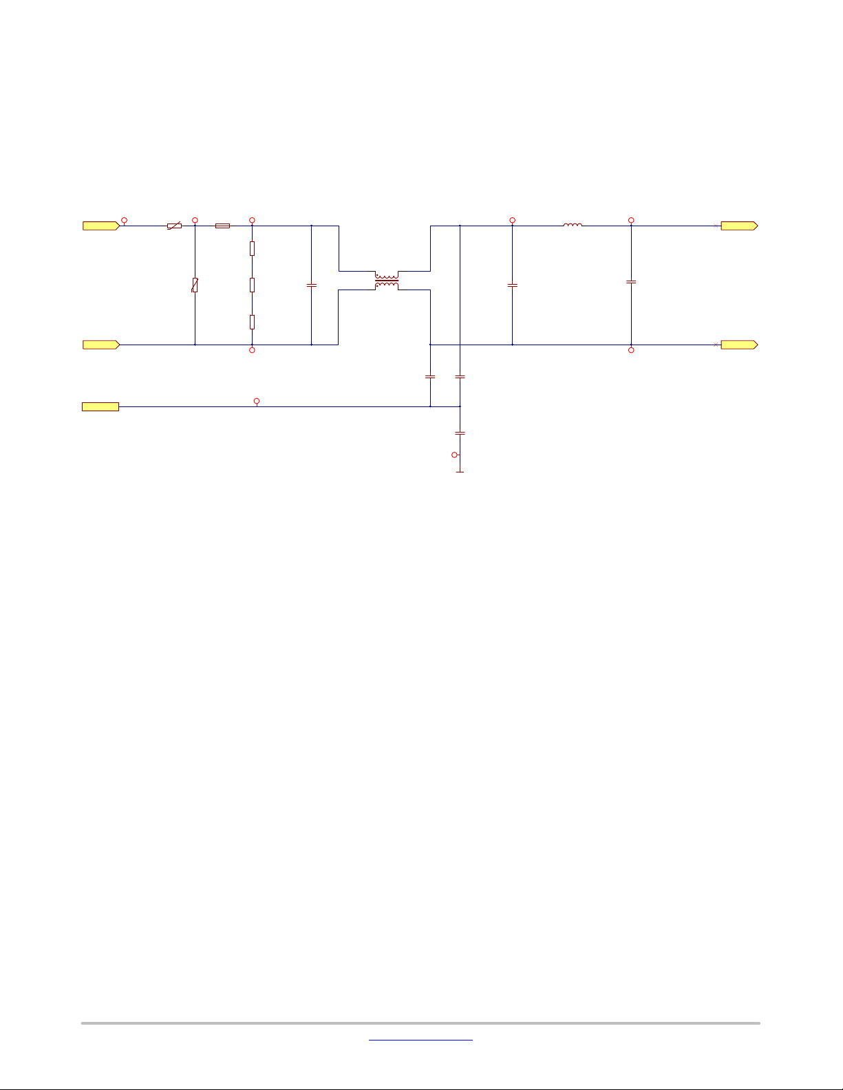
Figure 5. Schematic of EMI filter
Input EMI Filter
Figure 5 depicts schematic from AC input to rectifier
input. This circuitry include a passive EMI filter consisting
of elements C16, L5, CY1, CY3, CY4, C51, L4 and C17.
AC_IN
i
1−2
2−2
CY3
CY4
4700 pF
4700 pF
CY1
4700 pF
iGND
G_PFC
C51
680 nF
L4
150 mH
NEUTRAL_EMI_OUT
AC_IN
i
PHASE_EMI_OUT
C17
680 nF
i
NEUTRAL_IN
AC_L
AC_N
www.onsemi.com
6
Page 7
EVBUM2775/D
Interleaved PFC Stage
In higher power applications to utilize full capacity power
of mains and reduce harmonics is PFC−regulators generally
required. This high power application use interleaved PFC
stages, where may reduce inductor size, input and output
capacitors ripple current. In overall, power components are
smaller include capacitors. The NCP1632 as voltage mode
IC for interleaved PFC applications used in conduction
PHASE_PFC_IN
AC_L
AC_N
15VDC
D4
GBU6K
NEUTRAL_PFC_IN
15VDC
21
J2
C5
C6
100 nF
100 mF
C4
1 mF
soldered pads
C7
330 nF
R22
120k
R6
3M9
R12
3M9
R17
3M9
R21
3M9
R33
270k
DC_PFC_IN
R34
5k1
C15
1 nF
C13
68 pF
DC_IN
i
C11 C12
2m2
220 nF
R35
15k
R18
11k5
C3
100 nF
TP24
12
VCC
7
BO
4
OSC
5
VC
3
RT
15
REF5V
R32
22k
NCP1632
D9
MMSD4148T1G
R36
22k
R37
143k
U1
5 V reg
control
blocks
FFOLD
6
C14
470 nF
critical mode. It drives two mosfets 180° phase shifted. The
most important at design should be focused significant
inductance value of selected PFC coils. It significantly
specifies working range.
Figure 6 depicts schematic from rectifier input to DC link
output. Activation of stage (connection to 15 V DC power
supply) is via J2 (soldered pads).
D6
SMF15AT1G
CS
9
R26
1k8
13
ZCD1
DRV1
ZCD2
DRV2
Latch
OVP
GND
FB
TP27
D1
DCLINK_POS
8
2
R13
10k
R28
10k
1N5406RLG
TP23
i DC_IN
TR2
8
2
750314724
D2
FFSPF1065A
Q1
FCPF125N65S3
TR1
5
3
750314724
R10
22k
R11
22k
MMSD4148T1G
R7
10R
D3
16
TP25
R14
14
0R
1
TP26
R29
11
0R
10
2
8
R27
1k
C10
10 nF
Q2
MMBT589LT1G
MMSD4148T1G
D7
Q4
MMBT589LT1G
R25
10R
5
TP28
3
G_PFC
i DC_IN
D5
FFSPF1065A
Q3
FCPF125N65S3
TP1TP22
C42
470 mF
DCLINK_POS
R9
1M8
R16
1M8
R20
560k
R24
C9
27k
1 nF
DC_LINK
R8
1M8
R15
1M8
R19
820k
1 nF
R23
27kC8
G_PFC
G_PFC G_PFC
G_PFC
G_PFC
G_PFC G_PFC G_PFC G_PFC G_PFC
R31
R30
D8
0R075
0R075
NTSS3100
G_PFC
Figure 6. Schematic of interleaved PFC stage
G_PFC
G_PFC
G_PFC
G_PFC
G_PFC
www.onsemi.com
7
Page 8
EVBUM2775/D
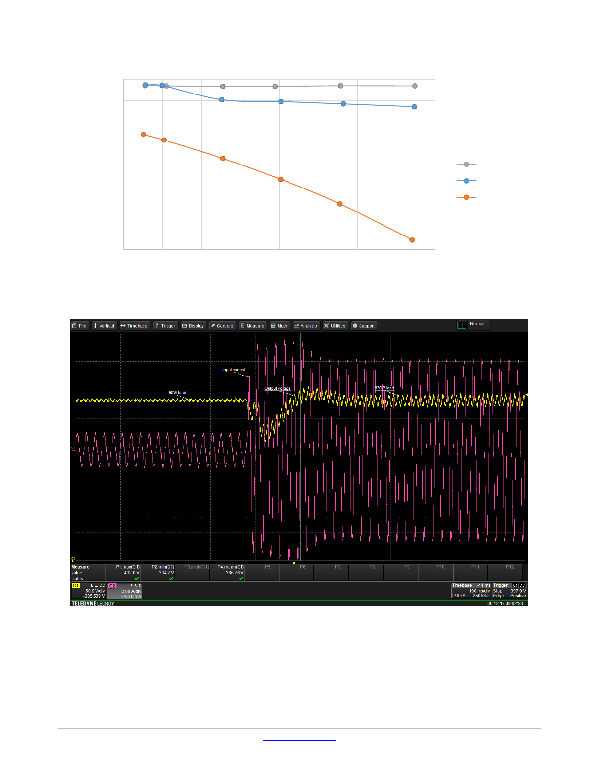
Basic tests and measurements were done. The results of
efficiency, power factor, power losses, load transients and
Efficiency PFC stage
97.00%
96.80%
96.60%
96.40%
96.20%
96.00%
95.80%
Efficiency [%]
95.60%
95.40%
95.20%
95.00%
190 200 210 220 230 240 250 260 270
Input AC voltage [V]
Figure 7. Efficiency of PFC Stage for Various Value of Input AC Voltage and Load
startup can be seen in the Figures 7−13. The used load was
Halogen light bulb.
930 W load
466 W load
155 W load
Efficiency [%]
Power factor PFC stage
0.998
0.978
0.958
0.938
0.918
0.898
0.878
0.858
0.838
190 200 210 220 230 240 250 260 270
Input AC voltage [V]
Figure 8. Power Factor of PFC Stage for Various Value of Input AC Voltage and Load
933 W load
466 W load
155 W load
www.onsemi.com
8
Page 9
0.998
0.978
0.958
0.938
EVBUM2775/D
Power factor PFC stage
0.918
0.898
Efficiency [%]
0.878
0.858
0.838
190 200 210 220 230 240 250 260 270
Input AC voltage [V]
Figure 9. Power Losses of PFC Stage for Various Value of Input AC Voltage and Load
933 W load
466 W load
155 W load
Figure 10. Load Transient 155 W to 930 W at 230 V AC Input
www.onsemi.com
9
Page 10

EVBUM2775/D
Figure 11. Load Transient 930 W to 155 W at 230 V AC Input
Figure 12. Start up to Open Circuit, 155 W and 930 W at 230 V AC Input
www.onsemi.com
10
Page 11

EVBUM2775/D
Figure 13. Start to 930 W at 230 V AC Input, Inrush Current
www.onsemi.com
11
Page 12

EVBUM2775/D
Auxiliary 15 V Power Supply
The NCP1063 is used as converter 390 V to 15 V output
to supply PFC, IPM and Control board (Arduino Due). The
maximal power delivered is up to 4.6 W. Figure 14 depicts
schematic of 15 V auxiliary power supply. Figure 15 shows
startup of the converter.
DC_LINK
C35
100 nF
L1
1 mH
DCLINK_POS
D14
MRA4007T3G
R47
G_PFC G_PFC G_PFC G_PFC
Figure 14. Schematic of Auxiliary 15V Power Supply
C36
10 mF
IC1
TP20
8
DRAIN
7
DRAIN
9 V reg
9V reg
control
block
3
LIM/OPP
5
COMP
TP21
1
C38
47 nF
GND
NCP1063AP60
D17
MURA160T3G
R49
15k
OTA
+
−
Vref
2.7 V
VCC
2
C1
10 mF
D15
MMSD4148T1G
R48
56k
C37
330 nF
R50
15k
L2
470 mH
D16
MURA160T3G
C39 C40
220 mF 220 mF
G_PFC
G_PFC G_PFC
C41
150 nF
G_PFC
TP3
15VDC
15VDC
R51
15k
C2
100 nF
4
FB
Figure 15. Start Up to Open Circuit, to 50 mA and to 300 mA at 390 V DC Input
www.onsemi.com
12
Page 13

EVBUM2775/D
IPM Stage
This stage uses NFAQ1060L36T IPM for 3−phase motor
drives containing three−phase inverter, gate drivers for the
inverter and a thermistor. It uses ON Semiconductor’s
Insulated Metal Substrate (IMS) Technology. Very
important function is over−current protection which is
deeply described in chapter – Current Measurement and
Over−Current Protection. Module also contains fault pin
which is keeping high level during normal state.
Activation
of IPM stage (connection to 15 V DC power supply) is via
J1 (soldered pads). In the figure 15 is shown schematics of
IPM stage also with DC link voltage measurement (voltage
divider containing R46, R52, R53 and R55). Signals from
39 mW shunt resistors are going to current measurement and
over−current protection circuits.
www.onsemi.com
13
Page 14

EVBUM2775/D
V_DCLINK
R53
330k
R52
330k
R46
330k
TP2
1
19
18
17
13
10
C_sense
C_SENSE
U_pos
V_pos
W_pos
R61
0R039
R60
0R039
R59
0R039
C43
1 nF
R62
10k
G_IPM
G_IPM
G_IPM
3PHASE_OUT
TP18
R55
6k8
AC_OUT
U2
NFAQ1060L36T
38
2
C18
G_IPM
i
250 nF
SMF15AT1G
C23 D11
C22
34
VB1
VB1
VCC
VCC
VCC
VDD
VDD
U_OUT
3PHASE_OUT
TP5
U
U_OUT
22 mF
100 nF
32
U,VS1
U, VS2
RCIN
12
V_OUT
TP9
V
i
AC_OUT
AC_OUT
IGBT
IGBT
HIN13HIN2
HIN1
V_OUT
i
SMF15AT1G
i
28
VB2
VCC
drivers
drivers
LIN16LIN27LIN38FAULT
AC_OUT
i
AC_OUT
C25 D12
22 mF
C24
100 nF
26
22
VB3
V,VS2
VCC
HIN3
HIN2
4
5
W
TP13
SMF15AT1G
C33 D13
22 mF
C32
100 nF
11
W_OUT
i
20
W,VS3
control
control
ENABLE
TP15
AC_OUT
W−
V−
U−
VSS
VSS
TH1
logic
ITRIP
TH2
9
14
TP16
R45
39k
R57
5k1
i
DCLINK_POS
DCLINK_POS
DC_LINK
G_IPM
21
J1
15VDC
15VDC
R44
2M
SMF15AT1G
D10
C21C20
soldered pads
330 mF
100 nF
NT3
NT2
NT1
R56
TP14
TP4
TP12
TP11
TP10
TP8
G_IPM G_IPM
TP7
TP6
1 2
1 2
G_PFC
R40 100R
R42 100R
R43 100R
HBW
HBW
LBW
LBW
R54 100R
ENABLE
ENABLE
R38 100R
R39 100R
1 2
HBU
HBU
IPM_CTRL
R41 100R
LBU
HBV
LBV
LBU
LBV
HBV
IPM CONTROL
5k1
C34
1 nF
100 pF
100 pF
100 pF
100 pF
100 pF
100 pF
100 pF
G_IPM
G_IPM
G_IPM
TP17
3V3
3V3
R58 100R
FAULT
TEMPERATURE
FAUL T
IPM_SENSE
V_DCLINK
V_DCLINK
TEMPERATURE
IPM_SENSE
ITRIP
C31
C30
C29
C28
C27
C26
C19
Figure 16. Schematic of IPM Stage
www.onsemi.com
14
Page 15

EVBUM2775/D
Current Measurement and Over−Current Protection
Schematic of current measurement and over−current
protection can be seen in the Figure 17. Information about
currents is provided via 39 mW shunt resistors. Voltage drop
from shunt resistor is going to input of operational amplifier
(op−amp) NCS2003 which gain is set to 4.99 with 1k resistor
and 4k99 resistor connected as negative feedback. U7
(TLV431) is creating 1.65 V reference which is connected
to non−inverting input of op−amps. This connection
provides voltage offset at the output of op−amps, which is
needed for negative current measurement.
Overcurrent protection is offered by NCS2250
comparator. Comparator threshold is set by voltage divider
which consists of R68, R71 and C48. Signals from shunt
resistors are going via R78, R81 and R84 connected to
non−inverting input. These resistors together with C58 are
also acting as low pass filter for high frequency signals
interference. On the one hand, with insufficient filtering the
over− current protection can react for lower values of current
even if there is 350 ns blanking time on ITRIP pin of IPM to
improve noise immunity (see datasheet of IPM). On the
other hand, when we are designing this filter it is needed to
be careful about the maximal time constant value according
short circuit safe operating area (see datasheet of IPM,
NFAQ1060L36T− for V
= 400 V is 4 ms). Output from
CE
comparator is connected to ITRIP pin of IMP module. As
was mentioned in previous chapter, IPM has fault pin and its
voltage level is high during normal state. An over−current
condition is detected if the voltage on the ITRIP pin is larger
than the reference voltage (typically 0.5 V). After a
shutdown propagation delay of typically 1.1 ms, the FAULT
output is switched on. The FAULT output is held on for a
time determined by the resistor and capacitor connected to
the RCIN pin (IPM pin 12). If R44 = 2 MΩ and C34 = 1 nF,
the FAULT output is switched on for 1.65 ms (typical). The
over−current protection threshold should be set to be equal
or lower to 2 times the module rated current. The reaction of
the protection can be seen in the Figure 18 and 19. System
is also using ENABLE pin of the IPM. After the
over−current fault, fault signal is generated and sent to
microcontroller which disable the IPM via ENABLE pin
(programmed by user). New operation is possible after
microcontroller reset.
3V3
C_SENSE
3V3
C_SENSE
U_pos
V_pos
W_pos
100 nF
R68
21.5 k
R74
3V3
4k99C52
U3
10 nF
G_IPM
C50
100 pF
C53
100 pF
C56
100 pF
C58
15 nF
NCS2003SN2T1G
3
4
R76
215k
NCS2250SN2T3G
3
IN+
4
IN−
R67
1k
R69
1k
R70
1k
R72
1k
R73
1k
R75
1k
R78
100R
R81
100R
R84
100R
R71
1kC48
IN+
IN−
52
OUT
G_IPM
R80
4k99
3V3
VDD
VSS
C49
C57
10 nF
100 nF
52
VDD
1
OUT
VSS
R83
4k99
U4
NCS2003SN2T1G
3
IN+
4
IN−
G_IPM
R85
4k99
3V3
52
OUT
VDD
VSS
C59
100 nF
1
C62
10 nF
G_IPM
C55
10 nF
R86
4k99
U5
NCS2003SN2T1G
3
IN+
4
IN−
G_IPM
R87
4k99
3V3
52
OUT
VDD
VSS
1
C63
100 nF
10 nF
C64
1V65
C61
47 mF
G_IPM
C54
10 nF
G_IPM
Q5
1
ITRIP
C60
10 nF
I_SENSE
I_U
I_U
I_V
I_V
I_SENSE
I_W
I_W
R77
680R
R79
1k
2
U7
K
TLV431
1
REF
A
3
R82
3k
G_IPM
G_IPM
G_IPM
G_IPM
Figure 17. Schematic of Current Measurement and Overcurrent Protection
www.onsemi.com
15
Page 16

EVBUM2775/D
Figure 18. Reaction of Over−current Protection
Figure 19. Reaction of Over−current Protection − Detail
www.onsemi.com
16
Page 17

EVBUM2775/D
Control Board Headers
Schematic of control board headers can be seen in the
Figure 20. The headers have Arduino Due footprint. The
applied control board has to contain 3V3 power supply as it
is also used for supplying current measurement op amps and
IPM_SENSE
FAUL T
FAUL T
IPM_SENSE
TEMPERATURE
I_SENSE
V_DCLINK
I_SENSE
V_DCLINK
TEMPERATURE
I_U
I_V
I_W
R64
R65
C47
1 nF
1k
1k
C46
470 pF
R66
1k
G_IPM G_IPM G_IPM G_IPM
R63
1k
C45
470 pF
comparator for over−current protection. Low pass filters for
current and voltage measurement signals are placed closed
to the headers (see CON4). When connecting the control
board to the PC, do not forget to use isolator.
12
34
6
C44
470 pF
1
2
3
4
5
6
7
8
CON4
G_IPM
5
8
7
10
9
12
11
14
13
16
15
17
18
19
20
2122
2324
26
25
28
27
30
29
32
31
34
33
36
35
CON3
IPM_CTRL
ENABLE
LBU
LBV
LBW
HBW
HBV
HBU
IPM CONTROL
3V3
3V3
1
2
3
4
5
6
7
8
CON6
15VDC
G_IPM
Figure 20. Schematic of Control Board Headers
Layout
Evaluation board consist of 4 layers. Following figures
are showing all the layers. Board size is 280x112 mm.
CON7
1
2
3
4
5
6
7
8
Figure 21. Top Layer Routing and Top Assembly
www.onsemi.com
17
Page 18

EVBUM2775/D
Figure 22. Internal Layer 1
Figure 23. Internal Layer 2
Figure 24. Bottom Layer Routing and Bottom Assembly
www.onsemi.com
18
Page 19

EVBUM2775/D
Electromagnetic Compatibility
Due to the inherent high frequency common mode noise
generated by the power switches, it is strongly
recommended to install a ferrite clamp on the motor wires.
Figure 25. Recommended EMC Filter
This will prevent disturbing other electronic devices in the
vicinity , including the UCB.
The recommended CM filter setup is depicted in the
picture below.
www.onsemi.com
19
Page 20

Bill of Materials
Table 3. BILL OF MATERIALS OF THE EVALUATION BOARD
No.
Designator
Comment
Manufacturer
Part number
Quantity
1.
C1
10 mF
Würth Electronik
865080540004
1
2.C2100 nF
Würth Electronik
885012206071
1
3.
C3, C5
100 nF
Würth Electronik
885012206095
2
4.
C4, C16
1 mF
Würth Electronik
890334026027CS
2
5.
C6
100 mF
Würth Electronik
875115652007
1
6.C7330 nF
Murata
GRM188R71C334JA01D
1
7.
C8, C9
1 nF
Würth Electronik
885012006044
2
8.
C10, C52, C54,
10 nF
Würth Electronik
885012206089
7
9.
C11
2m2
Würth Electronik
885012206027
1
10.
C12
220 nF
Murata
GRM188R71H224KAC4D
1
11.
C13
68 pF
Murata
GRM1885C1H680JA01D
1
12.
C14
470 nF
Murata
GRM188R61H474KA12D
1
13.
C15
1 nF
Würth Electronik
885012006063
1
14.
C17, C51
680 nF
Würth Electronik
890334026020CS
2
15.
C18
250 nF
TDK
B58031I9254M062
1
16.
C19, C26, C27,
100 pF
Würth Electronik
885012006057
10
17.
C20
100 nF
Würth Electronik
885012207072
1
18.
C21
330 mF
Würth Electronik
875075661010
1
19.
C22, C24, C32
100 nF
Würth Electronik
885012105018
3
20.
C23, C25, C33
22 mF
TDK
C4532X7R1E226M250KC
3
21.
C34, C43, C47
1 nF
Würth Electronik
885012206083
3
22.
C35
100 nF
Würth Electronik
890334025017CS
1
23.
C36
10 mF
Rubycon
450BXF10M10X16
1
24.
C37
330 nF
Würth Electronik
885012207101
1
25.
C38
47 nF
Würth Electronik
885012206093
1
26.
C39, C40
220 mF
Würth Electronik
860040474004
2
27.
C41
150 nF
Murata
GRM188R71H154KAC4D
1
28.
C42
470 mF
Würth Electronik
861141486024
1
29.
C44, C45, C46
470 pF
Würth Electronik
885012006061
3
30.
C48, C49, C59,
100 nF
Wurth Electronics
885012206046
4
31.
C58
15 nF
Würth Electronik
885012206090
1
32.
C60
10 nF
Würth Electronik
885012206065
1
33.
C61
47 mF
Murata
GRM188R60J476ME15D
1
34.
CON1
Black
TE Connectivity
6ESRM−P
1
35.
CON2
Green
Würth Elektronik
691313710003
1
36.
CON3
610 036 218 21
Würth Elektronik
61003621821
1
Table 3 provides bill of materials of the evaluation board.
C55, C57, C62,
C64
EVBUM2775/D
C28, C29, C30,
C31, C50, C53,
C56
C63
www.onsemi.com
20
Page 21

EVBUM2775/D
T
37.
CON4, CON6,
610 008 13 321
Würth Elektronik
61000813321
3
38.
CON5
691 313 510 002
Würth Elektronik
691313510002
1
39.
CY1, CY3, CY4
4700 pF
Murata
DE1E3KX472MA4BN01F
3
40.D11N5406RLG
ON Semiconductor
1N5406RLG
1
41.
D2, D5
FFSPF1065A
ON Semiconductor
FFSPF1065A
2
42.
D3, D7, D9, D15
MMSD4148T1G
ON Semiconductor
MMSD4148T1G
4
43.D4GBU6K
ON Semiconductor
GBU6K
1
44.
D6, D10, D11, D12,
SMF15AT1G
ON Semiconductor
SMF15AT1G
5
45.D8NTSS3100
ON Semiconductor
NTSS3100T3G
1
46.
D14
MRA4007T3G
ON Semiconductor
MRA4007T3G
1
47.
D16, D17
MURA160T3G
ON Semiconductor
MURA160T3G
2
48.F110 A
Schurter
0031.8201
1
49.F24 A
Schurter
0034.3123
1
50.
FC1
Fuse cover
Schurter
0853.0551
1
51.
HSA, HSB
SK 489 50 mm
2
52.
HSC
SK 92 30 mm
1
53.
HSD
SK 447 37.5 mm
1
54.
IC1
NCP1063AP60
ON Semiconductor
NCP1063AP60G
1
55.
J_AC_OUT
691 351 500 003
Würth Elektronik
691351500003
1
56.
J_DC390V
691 351 500 002
Würth Elektronik
691351500002
1
57.L11 mH
Würth Elektronik
744731102
1
58.
L2
470 mH
Würth Elektronik
744731471
1
59.
L4
150 mH
Würth Elektronik
7447076
1
60.L52 x 2.2 mH
Würth Elektronik
744824622
1
61.
NAC1, NAC2
nut M3 ISO4032
2
62.
Q1, Q3
FCPF125N65S3
ON Semiconductor
FCPF125N65S3
2
63.
Q2, Q4
MMBT589LT1G
ON Semiconductor
MMBT589LT1G
2
64.Q5NCS2250SN2T3G
ON Semiconductor
NCS2250SN2T3G
1
65.R12R2
TDK
B57237S0229M000
1
66.
R2, R4, R5
680k
Vishay
CRCW1206680KFKEA
3
67.
R3, R47
320 V
TDK
B72214S0321K101
2
68.
R6, R12, R17, R21
3M9
Vishay
CRCW12063M90FKEA
4
69.
R7, R25
10R
Panasonic
ERJ6ENF10R0V
2
70.
R8, R9, R15, R16
1M8
Vishay
CRCW12061M80FKEA
4
71.
R10, R11, R32,
22k
Panasonic
ERJ3EKF2202V
4
72.
R13, R28
10k
Panasonic
ERJ6ENF1002V
2
73.
R14, R29
0R
Panasonic
ERJ6GEY0R00V
2
74.
R18
11k5
Panasonic
ERJ3EKF1152V
1
able 3. BILL OF MATERIALS OF THE EVALUATION BOARD
No. QuantityPart numberManufacturerCommentDesignator
CON7
D13
black anodized
natural anodized
black anodized
R36
www.onsemi.com
21
Page 22

EVBUM2775/D
T
75.
R19
820k
Panasonic
ERJU08F8203V
1
76.
R20
560k
Panasonic
ERJU08F5603V
1
77.
R22
120k
Panasonic
ERJ3EKF1203V
1
78.
R23, R24
27k
Panasonic
ERJ3EKF2702V
2
79.
R26
1k8
Panasonic
ERJ3EKF1801V
1
80.
R27, R63, R64,
1k
Panasonic
ERJ3EKF1001V
6
81.
R30, R31
0R075
Bourns
CRA2512−FZ−R075ELF
2
82.
R33
270k
Panasonic
ERJ3EKF2703V
1
83.
R34, R56, R57
5k1
Panasonic
ERJ3EKF5101V
3
84.
R35, R49, R50,
15k
Panasonic
ERJ3EKF1502V
4
85.
R37
143k
Panasonic
ERJ3EKF1433V
1
86.
R38, R39, R40,
100R
Panasonic
ERJ3EKF1000V
11
87.
R442MVishay
CRCW06032M00FKEA
1
88.
R45
39k
Panasonic
ERJ3EKF3902V
1
89.
R46, R52, R53
330k
Vishay
CRCW1206330KFKEA
3
90.
R48
56k
Panasonic
ERJ3EKF5602V
1
91.
R55
6k8
Panasonic
ERJP08F6801V
1
92.
R59, R60, R61
0R039
KOA SPEER
TLRH3AWTTE39L0F
3
93.
R62
10k
Panasonic
ERJ3EKF1002V
1
94.
R66, R67, R69,
1k
Panasonic
ERJ3RBD1001V
7
95.
R68
21k5
Panasonic
ERJ3EKF2152V
1
96.
R74, R80, R83,
4k99
TT Electronics
PCF0603R−4K99BT1
6
97.
R76
215k
Panasonic
ERJ3EKF2153V
1
98.
R77
680R
Panasonic
ERJ3EKF6800V
1
99.
R82
3k
Panasonic
ERJ3EKF3001V
1
100.
SAC1, SAC2,
M3x8 DIN7985
7
101.
SB1, SB2, SB3,
Spacer M3 F/F 50
6
102.
SDA, SDB, SDD,
M3x16 DIN7985
7
103.
SHSA1, SHSA2,
spacer for M3
Wurth Elektronik
963030042
4
104.
ST1, ST2, ST3,
Spacer M3 M/F
6
105.
TP1, TP2
RED
Keystone
5005
2
able 3. BILL OF MATERIALS OF THE EVALUATION BOARD
No. QuantityPart numberManufacturerCommentDesignator
R65, R71, R79
R51
R41, R42, R43,
R54, R58, R78,
R81, R84
R70, R72, R73,
R75
R85, R86, R87
SHA1, SHA2,
SHB1, SHB2,
SHD1
SB4, SB5, SB6
SHC1, SHC2, SQA,
SQB
SHSB1, SHSB2
ST4, ST5, ST6
ELECTRONICS
HEX7
6/30 HEX7
Electronics
www.onsemi.com
22
Page 23

EVBUM2775/D
T
106.
TP3, TP17, TP24
ORANGE
Keystone
5008
3
107.
TP4, TP18, TP21
WHITE
Keystone
5007
3
108.
TP5, TP9, TP13,
BROWN
Keystone
5120
4
109.
TP6, TP7, TP8,
YELLOW
Keystone
5009
9
110.
TP15, TP16
BLUE
Keystone
5122
2
111.
TP20, TP23, TP28
PURPLE
Keystone
5124
3
112.
TP27
BLACK
Keystone
5006
1
113.
TR1, TR2
750314724
Würth Elektronik
750314724
2
114.U1NCP1632
ON Semiconductor
NCP1632DR2G
1
115.U2NFAQ1060L36T
ON Semiconductor
NFAQ1060L36T
1
116.
U3, U4, U5
NCS2003SN2T1G
ON Semiconductor
NCS2003SN2T1G
3
117.U7TLV431
ON Semiconductor
TLV431CSN1T1G
1
118.
WAC1, WAC2,
plain washer M3
14
119.
WHAD, WHAQ,
AOS 220
4
120.
WSDA, WSDB,
spring washer M3
5
Table 4. BILL OF MATERIALS OF THE UCB ADAPTER
No.
Designator
Comment
Manufacturer
Part number
Quantity
1.C110uF, 50V
Wurth Elektronik
885012108022
1
2.
C2, C11, C12
10uF, 10V
Wurth Elektronik
885012107010
3
3.C3100uF, 25V
Wurth Elektronik
865080449011
1
4.
C4, C5
100nF, 16V
Wurth Elektronik
885012206046
2
5.
C15, C21
10nF, 50V
Wurth Elektronik
885012206089
2
6.
C16
470nF, 50V
Wurth Elektronik
885012207102
1
7.
C19, C20
22uF, 10V
Wurth Elektronik
885012209006
2
8.
C23
470pF, 50V
Wurth Elektronik
885012006061
1
9.
D1, D2, D3, D4,
BAT54S
ON Semiconductor
BAT54S
10
10.
D11, D12
MBR230LSFT1G
ON Semiconductor
MBR230LSFT1G
2
11.
D13
MBRS2040LT3G
ON Semiconductor
MBRS2040LT3G
1
12.J161001011921
Wurth Elektronik
61001011921
1
13.
J2, J3, J5, J6, J7
61000811921
Wurth Elektronik
61000811921
5
14.J461003621821
Wurth Elektronik
61003621821
1
able 3. BILL OF MATERIALS OF THE EVALUATION BOARD
No. QuantityPart numberManufacturerCommentDesignator
Electronics
Electronics
TP22
TP10, TP11, TP12,
TP14, TP25, TP26
WHSA1, WHSA2,
WHSB1, WHSB2,
WPDA, WPDB,
WPDD, WPQA,
WPQB, WSHC1,
WSHC2, WSHD1
WHBD, WHBQ
Electronics
Electronics
Electronics
Electronics
Electronics
DIN125A
18x12x1.5 D3.1
WSDD, WSQA,
WSQB
D5, D6, D7, D8,
D9, D10
DIN7980
www.onsemi.com
23
Page 24

EVBUM2775/D
15.J861000621821
Wurth Elektronik
61000621821
1
16.J9694106105102
Wurth Elektronik
694106105102
1
17.
JB1, JB2
10139781−121402LF
Amphenol
10139781−121402LF
2
18.L122uH, 3A
Wurth Elektronik
7447714220
1
19.
R1, R60R 2
20.
R30R 1
21.
R4
270R
1
22.
R5
560R
1
23.
R7, R8
470R
2
24.
R45
22k
1
25.
R463k 1
26.
R47
56k
1
27.U1FAN8303MX
ON Semiconductor
FAN8303MX
1
28.U2NCP1117ST33T3G
ON Semiconductor
NCP51460SN33T1G
1
29.U3NCP1117ST50T3G
ON Semiconductor
NCP1117ST50T3G
1
30.C110uF, 50V
Wurth Elektronik
885012108022
1
31.
C2, C11, C12
10uF, 10V
Wurth Elektronik
885012107010
3
32.C3100uF, 25V
Wurth Elektronik
865080449011
1
33.
C4, C5
100nF, 16V
Wurth Elektronik
885012206046
2
34.
C15, C21
10nF, 50V
Wurth Elektronik
885012206089
2
35.
C16
470nF, 50V
Wurth Elektronik
885012207102
1
36.
C19, C20
22uF, 10V
Wurth Elektronik
885012209006
2
37.
C23
470pF, 50V
Wurth Elektronik
885012006061
1
38.
D1, D2, D3, D4,
BAT54S
ON Semiconductor
BAT54S
10
39.
D11, D12
MBR230LSFT1G
ON Semiconductor
MBR230LSFT1G
2
40.
D13
MBRS2040LT3G
ON Semiconductor
MBRS2040LT3G
1
41.J161001011921
Wurth Elektronik
61001011921
1
42.
J2, J3, J5, J6, J7
61000811921
Wurth Elektronik
61000811921
5
43.J461003621821
Wurth Elektronik
61003621821
1
44.J861000621821
Wurth Elektronik
61000621821
1
45.J9694106105102
Wurth Elektronik
694106105102
1
46.
JB1, JB2
10139781−121402LF
Amphenol
10139781−121402LF
2
47.L122uH, 3A
Wurth Elektronik
7447714220
1
48.
R1, R60R 2
49.
R30R 1
50.
R4
270R
1
51.
R5
560R
1
52.
R7, R8
470R
2
53.
R45
22k
1
54.
R463k 1
55.
R47
56k
1
56.U1FAN8303MX
ON Semiconductor
FAN8303MX
1
57.U2NCP1117ST33T3G
ON Semiconductor
NCP51460SN33T1G
1
58.U3NCP1117ST50T3G
ON Semiconductor
NCP1117ST50T3G
1
Table 4. BILL OF MATERIALS OF THE UCB ADAPTER
No. QuantityPart numberManufacturerCommentDesignator
D5, D6, D7, D8,
D9, D10
www.onsemi.com
24
Page 25

EVBUM2775/D
GRAPHICAL USER INTERFACE
Open loop operation (V/F)
In order to facilitate fast evaluation of the power stage, the
user can select open loop operation option within the GUI
menu.
FOC closed loop operation
Modern control drives implement the well−known Field
Oriented Control (FOC) control−strategy; FOC provides
efficient motor−drive for a wide range of motor−speeds, fast
dynamic response, a low harmonic content of currents, and
reduced losses [8−10].
In general, the implementation of FOC requires at least:
• 1 Timer
• 4 ADC channels (see Note below)
• USART/SPI for communications
• Capture/PWM
FOC should achieve:
• High control bandwidth
• Low current distortion
• Control capability at low speeds
Figure 26. Graphical User Interface for Controlling the Motor in the Open Loop
NOTE: One channel for the voltage level of the VSI H−Bridge, and three channels for the – three – phase currents that flow
towards the motor. However, it is possible to implement the FOC strategy with only three ADC channels (two
channels for current and one channel for the voltage), as we can measure two−phase currents and mathematically
calculate the third one. That implementation requires one shunt−resistor less. Compact IPM, thought, comes
already with three shunt−resistors.
www.onsemi.com
25
Page 26

EVBUM2775/D
During the communication with control board and PC,
using of USB isolator is very important because of safety.
In the Figure 27 can be seen evaluation board with USB
isolator (5 kV optical isolation).
Figure 27. Evaluation Board with Control Board and USB Isolator
www.onsemi.com
26
Page 27

EVBUM2775/D
REFERENCES
[1]. Datasheet of IPM NFAQ1060L36T, available on
ON Semiconductor website
[2]. Datasheet of NCP1632, available on
ON Semiconductor website
[3]. Application note − Key Steps to Design an
Interleaved PFC Stage Driven by the NCP1632,
available on ON Semiconductor website
[4]. Datasheet of NCP1063, available on
ON Semiconductor website
[5]. Application note − Universal AC Input, 12V
0.35 A Output, 4.2 Watt Non−isolated Power
Supply, available on ON Semiconductor website
[6]. Datasheet of NCS2003, available on
ON Semiconductor website
[7]. Datasheet of NCS2250, available on
ON Semiconductor website
[8]. J.A. Santisteban, R.M. Stephan, “Vector control
methods for induction machines: an overview,”
IEEE Transactions on Education, Vol 44, no 2,
pp−170−175, May 2001.
[9]. M. Ahmad, “High Performance AC Drives:
Modelling Analysis and Control,” published by
Springer−Verlag, 2010.
[10]. J.R Hendershot, T.J.E. Miller, “Design of
Brushless Permanent−Magnet Machines,”
published in the USA by Motor Design Books
LLC, 2010.
www.onsemi.com
27
Page 28

ON Semiconductor and the ON Semiconductor logo are trademarks of Semiconductor Components Industries, LLC dba ON Semiconductor or its subsidiaries in the United States and/or
other countries. ON Semiconductor owns the rights to a number of patents, trademarks, copyrights, trade secrets, and other intellectual property. A listing of ON Semiconductor’s
product/patent coverage may be accessed at www.onsemi.com/site/pdf/Patent−Marking.pdf
subject to all applicable copyright laws and is not for resale in any manner.
The evaluation board/kit (research and development board/kit) (hereinafter the “board”) is not a finished product and is as such not available for sale to consumers. The board is only intended
for research, development, demonstration and evaluation purposes and should as such only be used in laboratory/development areas by persons with an engineering/technical training
and familiar with the risks associated with handling electrical/mechanical components, systems and subsystems. This person assumes full responsibility/liability for proper and safe handling.
Any other use, resale or redistribution for any other purpose is strictly prohibited.
The board is delivered “AS IS” and without warranty of any kind including, but not limited to, that the board is production−worthy, that the functions contained in the board will meet your
requirements, or that the operation of the board will be uninterrupted or error free. ON Semiconductor expressly disclaims all warranties, express, implied or otherwise, including without
limitation, warranties of fitness for a particular purpose and non−infringement of intellectual property rights.
ON Semiconductor reserves the right to make changes without further notice to any board.
You are responsible for determining whether the board will be suitable for your intended use or application or will achieve your intended results. Prior to using or distributing any systems
that have been evaluated, designed or tested using the board, you agree to test and validate your design to confirm the functionality for your application. Any technical, applications or design
information or advice, quality characterization, reliability data or other services provided by ON Semiconductor shall not constitute any representation or warranty by ON Semiconductor,
and no additional obligations or liabilities shall arise from ON Semiconductor having provided such information or services.
The boards are not designed, intended, or authorized for use in life support systems, or any FDA Class 3 medical devices or medical devices with a similar or equivalent classification in
a foreign jurisdiction, or any devices intended for implantation in the human body. Should you purchase or use the board for any such unintended or unauthorized application, you shall
indemnify and hold ON Semiconductor and its officers, employees, subsidiaries, affiliates, and distributors harmless against all claims, costs, damages, and expenses, and reasonable
attorney fees arising out of, directly or indirectly, any claim of personal injury or death associated with such unintended or unauthorized use, even if such claim alleges that ON Semiconductor
was negligent regarding the design or manufacture of the board.
This evaluation board/kit does not fall within the scope of the European Union directives regarding electromagnetic compatibility, restricted substances (RoHS), recycling (WEEE), FCC,
CE or UL, and may not meet the technical requirements of these or other related directives.
FCC WARNING – This evaluation board/kit is intended for use for engineering development, demonstration, or evaluation purposes only and is not considered by ON Semiconductor to
be a finished end product fit for general consumer use. It may generate, use, or radiate radio frequency energy and has not been tested for compliance with the limits of computing devices
pursuant to part 15 of FCC rules, which are designed to provide reasonable protection against radio frequency interference. Operation of this equipment may cause interference with radio
communications, in which case the user shall be responsible, at its expense, to take whatever measures may be required to correct this interference.
ON Semiconductor does not convey any license under its patent rights nor the rights of others.
LIMITATIONS OF LIABILITY: ON Semiconductor shall not be liable for any special, consequential, incidental, indirect or punitive damages, including, but not limited to the costs of
requalification, delay, loss of profits or goodwill, arising out of or in connection with the board, even if ON Semiconductor is advised of the possibility of such damages. In no event shall
ON Semiconductor’s aggregate liability from any obligation arising out of or in connection with the board, under any theory of liability, exceed the purchase price paid for the board, if any.
For more information and documentation, please visit www.onsemi.com
.
. ON Semiconductor is an Equal Opportunity/Affirmative Action Employer. This literature is
PUBLICATION ORDERING INFORMATION
LITERATURE FULFILLMENT:
Email Requests to: orderlit@onsemi.com
ON Semiconductor Website: www.onsemi.com
TECHNICAL SUPPORT
North American Technical Support:
Voice Mail: 1 800−282−9855 Toll Free USA/Canada
Phone: 011 421 33 790 2910
Europe, Middle East and Africa Technical Support:
Phone: 00421 33 790 2910
For additional information, please contact your local Sales Representative
◊
www.onsemi.com
1
 Loading...