

Page 1

EVBUM2516/D
150 W High Power Density
Adapter Using SJ Si
MOSFETs Evolution Board
User Manual
www.onsemi.com
Contents
This evaluation board user manual describes the 150 W
High Power Density Adapter and its main parameters like
efficiency, no−load input power consumption, EMI
signature, transient responses, etc. The evaluation board is
dedicated to present ON Semiconductor’s high performance
controllers. High Power Density design is enabled when
using these controllers and higher switching frequency.
Higher efficiency can be achieved by using GaN HEMT
devices instead of Silicon Super−junction MOSFETs.
The evaluation board comprising of the PFC boost
converter operated in the critical conduction mode (CrCM)
and LLC power stage. The PFC front stage is driven by
NCP1615, assures unity power factor and low input current
THD. The LLC stage operates @ 260 to 300 kHz @ nominal
load and it’s managed by the NCP1399 high performance
current mode LLC controller. Super−junction Si MOSFETs
(like FCMT199N60) can be assembled as primary side
power switches. The CV/CC controller NCP4353A ensures
output voltage regulation.
Above mentioned controllers are placed on the Control
Module. Secondary side utilizes synchronous rectifier (SR)
from NCP4305 or NCP4306 family composed with
NVMFS5C645NL 4mW 60V Power MOSFET. Whole SR
stage is implemented on the daughter card for easier main
power board PCB design. The discrete or integrated LLC
resonant thanks implementations can be used in one board
with few changes thanks to universal design.
EVAL BOARD USER’S MANUAL
This evaluation board manual focuses mainly on short
description of adapter operation principles and connections.
For more detailed information please refer to datasheets of
individual part.
Key Features
• Wide Input Voltage Range
• High Power Density, High Efficiency
• Low No−load Power Consumption
• X2 Capacitor Discharge Function
• Near Unity Power Factor
• Overload Protection, Thermal Protection
• Low Mains Operation Protection
• Secondary Short Circuit Protected
• Regulated Output Under any Conditions
• Capability to Implement Off−mode for
Table 1. GENERAL PARAMETERS
Device Applications Input Voltage
NCP1615
NCP1399
NCP4305
NCP4353
Efficiency Standby Power
Up to 94.15%
© Semiconductor Components Industries, LLC, 2016
October, 2017 − Rev. 6
Notebook
Adaptors,
Ac – dc converters
for consumer
electronics
150 mW @ 230
Vac
Normal Output
Voltage / Current
90 – 265 Vac
Operating
Temperature
0 – 50 °C Passive cooling
19 Vdc / 8 A
9 A max limit
Cooling Topology Board size
1 Publication Order Number:
Output Power V
150 W < 250 mV @ Full load
PFC CrCM
LLC + SR
Ripple
OUT
116 x 55 x 18 mm
EVBUM2516/D
Page 2
EVBUM2516/D
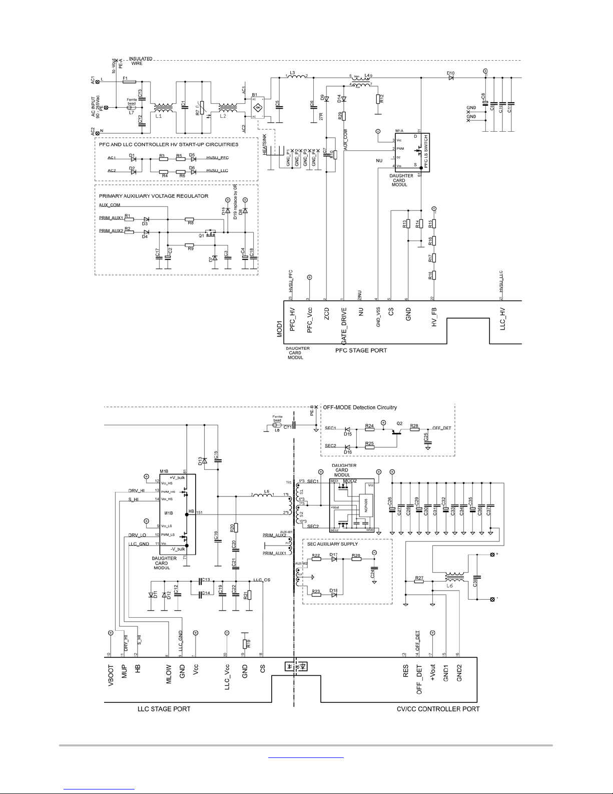
Figure 1. 150 W High Power Density Adapter − Schematic Of The Power−Board (1/2)
Figure 2. 150 W High Power Density Adapter − Schematic Of The Power−Board (2/2)
www.onsemi.com
2
Page 3

EVBUM2516/D
Figure 3. High Power Density Adapter − Schematic Of The Control Module 1/2
www.onsemi.com
3
Page 4
EVBUM2516/D
Figure 4. High Power Density Adapter − Schematic Of The Control Module 2/2
www.onsemi.com
4
Page 5
EVBUM2516/D
Figure 5. 150 W High Power Density Adapter − Schematic Of The Switch Module With Si MOSFETs
Figure 6. 150 W High Power Density Adapter − Schematic of Synchronous Rectifier Module
www.onsemi.com
5
Page 6
EVBUM2516/D
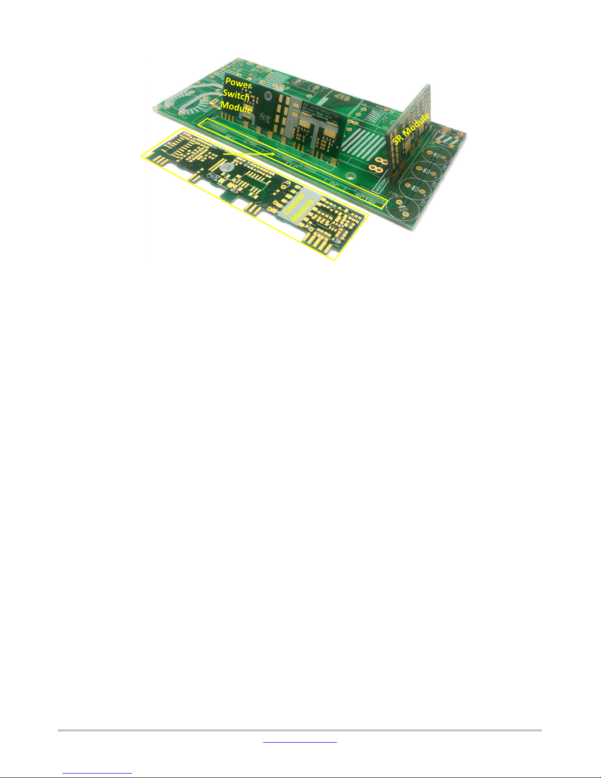
Figure 7. 150 W High Power Density Adapter − Arrangement Of Modules
DETAILED DESCRIPTIONS OF THE EVALUATION
BOARD
Adapter modular conceptions − The demo−board is
constructed using a main power board plus daughtercards or
modules, which are showed in Figure 7. This assists
evaluation and allows the user to exchange daughtercards
for experimentation. This comprehensive type of
construction helps to reduce PCB area, thus increases power
density and also allows reducing number of PCB layers. All
modules PCBs are designed as 2−layers with 35um or 70um
thin copper plating. PCBs with 70um copper plating are used
for SR and Power Switch Modules. The lowest PCB
manufacturing and assembly cost has been achieved thanks
to this construction.
The input of the converter is protected by the varistor
R7. A differential mode lighting surge protection has not
been optimized. The fuse F1 is 4A time−lag type fuse to
withstand the inrush current. The inrush current limiting
NTC thermistor is not used in this demo−board (Figure
NO TAG.)
The EMI filter consists from the common−mode power
line chokes L1 and L2, X2−capacitor C1, and three
Y−capacitors CY1 − CY3. CY1 is complemented with
ferrite beads L6 at one terminal. The center of CY2 and CY3
capacitors is connected to the PE terminal through ferrite
bead L7. The PE−A terminal should be connected to the
PE−B terminal by a wire to reduce EMI signature. Pre−filter
arranged by polypropylene capacitors C5, C6 and
differential mode inductor L3 (Figure NO TAG.) is used for
further reduction of EMI signature.
The HV Start−up and X2 discharge capability – both
primary controllers are equipped with High Voltage
Start−up current sources (NCP1615, NCP1399). PFC
High−voltage Start−up (HVSU) is assured via serial circuit
R3, R5, D5, and two diodes D1 and D2. Diodes are shared
for PFC and LLC HVSU. LLC HVSU is joined through
same serial circuit R4, R6 and D6. To avoid influence
between controllers, HV pin of both controllers are
separated via mentioned serial circuitries.
Additionally for NCP1615 – the PFC controller has X2
discharge function. The X2−capacitor is discharged after
disconnecting power cord from the line.
The PFC front stage implements critical conduction
mode PFC boost converter and consists mainly the bulk
capacitor C8, which is decoupled at high frequencies (HF)
with multi−layer ceramic capacitors (MLCC) C9−11, PFC
inductor L4, rectifying diode D10 and power switch (Figure
NO TAG.), which is located on Power Switch Module
(Figure 5.). The PFC controller NCP1615 senses inductor
current directly as a voltage drop on resistors R13, R14.
These resistors are connected directly to Control Module,
where the PFC controller is located. These resistors define
maximum PFC front stage peak current. The PFC controller
U1 (NCP1615) uses CS/ZCD for inductor peak current
sensing and zero current condition or valley detection. Zero
current detection is guaranteed by PFC coil auxiliary
winding voltage, which is rectified with D9 and this signal
is connected to Control Module via parallel RC circuit R10
and C7. Input voltage is observed at HV pin, which also
serves for input voltage sensing and BROWN−OUT
protection. The bulk capacitor voltage is fed into PFC
controller through set of four resistors R15, R16, R17 and
R18. Necessary PFC compensation circuitries and
components are located on the Control Module board. The
PFC OK status is transferred via network of C9, R13, C13
and R18 to LLC controller, which is subsequently enabled
after PFC provides PFC OK status. For more details, please
refer to NCP1615 datasheet.
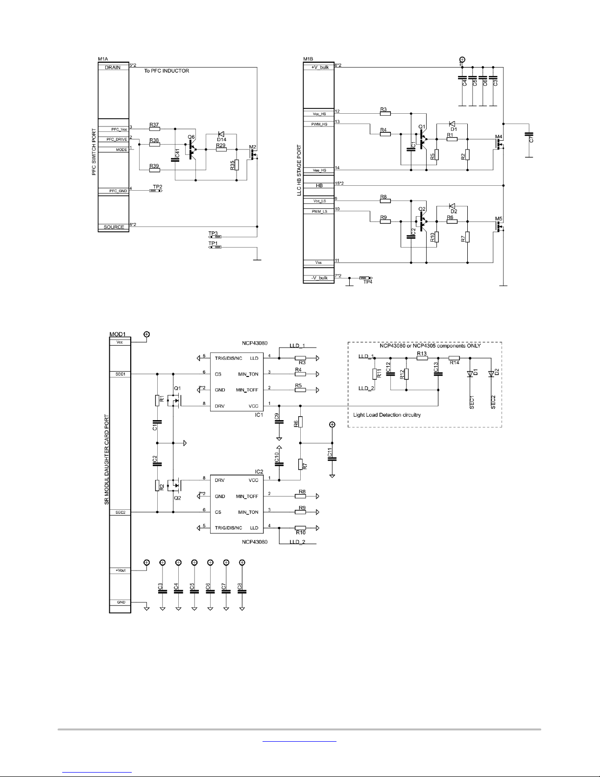
Power Switch Module with Si SJ MOSFETs is showed
in Figures 5, 15, 16. Power Switch Module consists of power
www.onsemi.com
6
Page 7

EVBUM2516/D
FET devices and additional components which are
necessary for correct operation.
Power Switch Module is designed for Silicon Power
MOFETs in small SMD package so−called the Power88. In
Figure 6 is Power Switch module schematic, where M2 is
the low side switch of PFC front stage, M4 and M5 create
LLC half−bridge stage. C3, C4, C5, C6 and C7 are HF
decoupling MLCC capacitors with same function as afore
mentioned. Q1, Q2, Q6 forms emitter followers with Vcc
decoupling capacitors C1, C2 and C41. Emitter followers
provide buffering of driving signal in case of need – they can
be assembled on purpose. Paralleled resistor−diode pairs
(D14–R29, D1–R1, D2–R6) set switching slopes of
MOSFETs and this way improving EMI signature.
Exchange of Power Switch Modules Important notes
– Power Switch Modules can be exchanged, but specific
conditions must be satisfied due to operation differences:
Silicon MOSFETs requirements:
• Higher magnetizing current (compare to GaN) to
achieve ZVS ³ Lower magnetizing inductance
because of higher output capacitance
• Maximum needed Dead−time up to 500ns
• Maximum switching Frequency is limited from to 420
– 450kHz @Light−load − it is given by used MOSFET
parameters
• Dedicated NCP1399 setting is needed for Si MOSFETs
board option
GaN FETs requirements:
• Lower magnetizing current (compare to Si MOSFETs)
to achieve ZVS ³ Higher magnetizing inductance, less
conduction losses
• Maximum needed Dead−time ~200ns
• Frequency is limited by IC controller
• Dedicated NCP1399 setting is needed for GaN
MOSFETs board option
To summarize: the LLC controller has to be replaced and
air gap in the LLC transformer increased when Switching
Module is changed from GaN to ³ Si type.
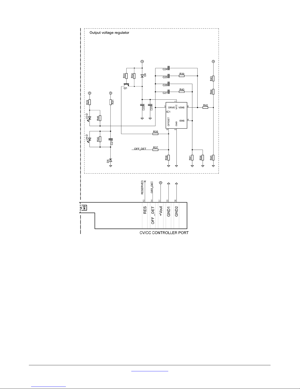
Control Module – (Figures NO TAG, NO TAG, 13, 14)
integrates the PFC controller NCP1615, the LLC controller
NCP1399 and secondary side CV/CC controller NCP4353
in one PCB. Control module is designed in such a way, that
each component is placed to its dedicated controller as close
as possible. Another design strategy was to move all signal
processing components to the Control Module, except the
high voltage circuitries for example bulk voltage feedback
divider. Module also contains two optocouplers, first one
output is used for voltage feedback loop. IC1 – NCP4353
(Figure NO TAG) senses output voltage using resistor
divider R43, R44 and R45 and transfers this information via
optocoupler U3 to primary side, to the U2 – NCP1399,
which regulates switching frequency according to feedback
and current sense signals. Second optocoupler is dedicated
to output overvoltage protection (OVP). As soon as output
voltage reaches ~21V, optocoupler U4 pulls up OVP/OTP
pin of U2 and activates OVP. Output OVP level and response
is defined by zener diode D5, resistors R30, R31 and
capacitor C21.
The LLC primary stage is formed by half−bridge, which
is located on the Power switch Module, split resonant tank
capacitors C15−C16, clamping diode D13, resonant
inductor L5 (in case of discrete resonant transformer
implementation) and transformer TR1. The resonant
capacitor voltage divided down by R20, R21, C12, C13,
C14, C19, C20, C21, C22, D11 and D12 and provides
information about transformer current for NCP1399.
Divider serves as current feedback loop and also sets adapter
output current limit.
The Synchronous Rectifier Module (Figures 6, 17, 18)
consists of two Single N−Channel SO−8FL Logic Level
60V MOSFETs Q1 and Q2, two synchronous rectifier (SR)
controllers IC1−2 NCP43080 (or similar part from
NCP430x family) and HF decoupling MLCC capacitors
C3−8. RC snubber circuits, composed as R1−C1 and R2−C2,
are connected across the drain and the source of each
MOSFET, to protect them against voltage spikes. C9−11 and
R6−7 are components use to filtering and HF decoupling
supply voltage for both SR controllers. R4 (R9) and R5 (R8)
serve to set minimum ON and minimum OFF switching
times of SR controller. Automatic Light Load and Disable
mode (LLD pin) is input modulates the driver clamp level
and/or turns the driver off during light load conditions. This
feature helps to reduce No−load consumption and improves
Light−load efficiency. In Figure 6, the Light−Load
Detection Circuitry is formed by resistors R11–14, ceramic
capacitors C12, C13 and diodes D1−2. If there is a certain
reason to not use LLD feature, use R3 (R10) zero ohms to
disable it. Then in this situation Light−Load Detection
Circuitry doesn’t have to be assembled. When using
NCP4306, R3 (R10) resistors can set specific timing of
Automatic LLD or disable it fully and external Light−Load
Detection Circuitry is not needed anymore. For more detail
please see each device specific datasheet.
The regulation of output voltage is ensured by the
regulator IC1–NCP4353 (see Figure NO TAG), which
provides integrated voltage feedback regulation, replacing
traditional shunt regulator. The device is capable of
detecting “no−load” conditions and inserts the power supply
into a low consumption OFF−
current regulation loop in addition to voltage regulation.
These possibilities are included in design of PCBs, but
demo−board is not utilized them. The optocoupler U3 is
driven via resistor R29, which determines the feedback loop
gain. Resistor R46 biases the NCP4353 in case that there is
no current flowing through the optocoupler U3. The voltage
feedback loop compensation network is created by resistors
R39, R42 capacitors C24, C25. The value of output voltage
is set up by voltage divider comprised of resistors R43, R44,
R45.
mode. IC1 also includes a
www.onsemi.com
7
Page 8
EVBUM2516/D
Coupling between primary and secondary is ensured
by the Y−capacitor CY1, which is connected between
secondary ground and primary bulk voltage. Similar
functionality have CY2 and CY3, which are placed between
input terminals (L, N) and their center point is connected to
PE earth terminal. PE−A and PE−B allow making the
PBC Layout
The PCB is made as a double layer FR4 board with 35mm
copper cladding.
connection between secondary ground GND and input earth
terminal (PE). The connection should be made by awg 18 or
0.75 mm
2
wire with optionally threaded ferrite bead.
This configuration of CY1−3 helps to improve the EMI
signature of the converter and pass legislation EMI emission
limits.
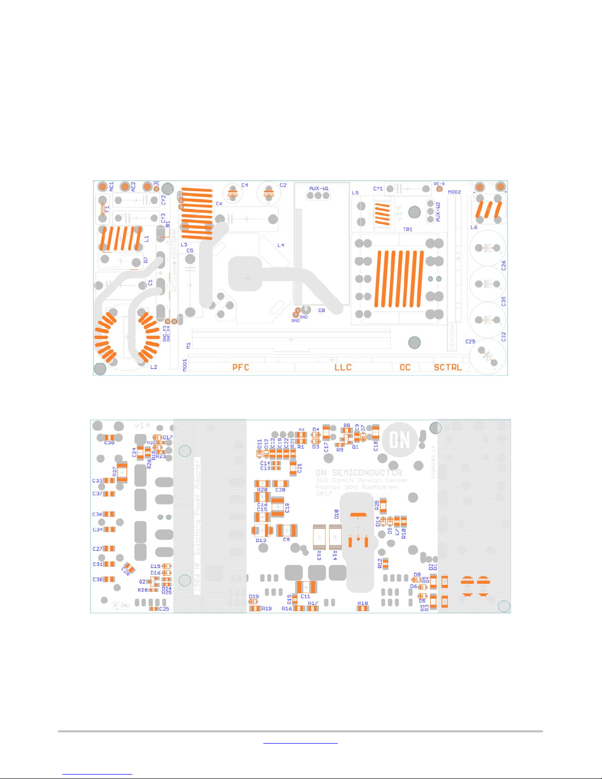
Figure 8. Evaluation Board − Top Side Components
Figure 9. Evaluation Board − Bottom Side Components
www.onsemi.com
8
Page 9

EVBUM2516/D
Figure 10. Evaluation Board − Top Layer Red, Bottom Layer Blue
Figure 11. Evolution Board Photograph − Bottom Side
www.onsemi.com
9
Page 10

EVBUM2516/D
Figure 12. Evolution Board Photograph − Top View
Figure 13. Control Module − Top Side Components, Top Layer − Red,
Bottom Layer − Blue
www.onsemi.com
10
Page 11

EVBUM2516/D
Figure 14. Control Module Photograph
Figure 15. Power Switch Module, Top Side Components, Top Layer − Red,
Bottom Layer − Blue
Figure 16. Power Switch Module Photograph
www.onsemi.com
11
Page 12

EVBUM2516/D
Figure 17. SR Module, Top Side Components, Top Layer − Red,
Bottom Layer − Blue
Figure 18. SR Module Photograph
www.onsemi.com
12
Page 13

EVBUM2516/D
Figure 19. Resonant Tank Composition And Power Switch Module
Selection Procedures
www.onsemi.com
13
Page 14

MEASUREMENTS
The measurements show the performance of High Power
Density Demo−board.
95
90
85
80
75
70
Efficiency [%]
65
60
55
50
0 20 40 60 80 100 120 140 160
EVBUM2516/D
Efficiency vs. Output power
Si based solution with Integrated LLC transformer, 90VAC
Si based solution with Integrated LLC transformer, 120VAC
Si based solution with Integrated LLC transformer, 230VAC
Output power [W]
Figure 20. Efficiency Graph Of High Power Density Demo−Board*
NOTES: *Measured with IPL60R255P6 placed in PFC
and LLC stages
Table 2. EFFICIENCY TABLE
Output power level [%] 10% 25%
81.24 89.42 91.74 91.72 90.90 91.93 91.14
Efficiency [%] @
Input voltage [V
RMS
90
120 81.90 90.07 92.49 92.88 92.52 92.90 92.17
]
230 82.87 91.72 93.80 94.14 94.03 94.15 93.57
Table 3. STANDBY POWER TABLE
Input voltage [Vms] 90 120 230 265
Standby power [mW] 149 (Note 1, 2) 152 (Note 1, 2) 150 (Note 1, 2) 150 (Note 1, 2)
1. Measured with Tektronix PA1000 Power Analyzer and the integration mode was used.
2. Still exists place for no−load optimalisation.
50% 75%
100% Max efficiency
Calculated
4−point avg.
efficiency
www.onsemi.com
14
Page 15

EVBUM2516/D
25
30
35
40
45
50
55
60
65
70
100 000
Frequency [Hz]
Conducted Emission Quasi −peak dBmV (Domestic)
Limit quasi−peak
Si Based Solution, 230VAC@Full−load, optimized
0.1MHz
2MHz
5MHz
9MHz
30MHz
0.1MHz
Figure 21. EMI Signature Comparison @ 230 VAC (Measured MAX Peak)
i
(t)
out
V
(t)
out DC
V
(t)
out AC
Figure 22. Transition Response − I
= 0 A to 8 A, VIN = 120 V,
OUT
www.onsemi.com
15
Page 16

EVBUM2516/D
(t)
i
out
V
OUT_DC
(t)
OUT_AC
(t)
V
Figure 23. Transition Response − I
= 8A to 0 A, VIN = 120 V,
OUT
V
PFC_DRV
(t)
CS_ZCD
V
DS
(t)
(t)
V
Figure 24. PFC − Input Current Modulation, I
www.onsemi.com
16
= 7 A, VIN = 120 V,
OUT
I
PFC_indutor
(t)
Page 17

EVBUM2516/D
V
PFC_DRV
VCS_
V
(t)
DS
ZCD
(t)
i
PFC_indutor
(t)
Figure 25. PFC Operating Waveforms, I
(t)
= 7 A, VIN = 120 V,
OUT
LLC_HB
(t)
i
tank
V
(t)
V
VFR(t)
(t)
FB
(t)
V
CS
Figure 26. LLC − Stage Normal Operation Waveforms, I
= 8A (Full−load)
OUT
www.onsemi.com
17
Page 18

V
LLC HB
VCS(t)
i
tank
VFB(t)
EVBUM2516/D
(t)
VDS_
VDS_
SRI
SR2
Figure 27. LLC Stage SKIP MODE Operation Waveforms, I
(t)
I
SD_SR2
(t)
I
SD_SR1
= 600 mA
OUT
(t)
Figure 28. Synchronous Rectifier Operating Waveforms − SKIP MODE I
= 120 V,
V
IN
www.onsemi.com
18
= 100 mA,
OUT
Page 19

EVBUM2516/D
(t)
V
DS_SRI
I
(t)
SD_SR1
Figure 29. Synchronous rectifier operating waveforms, I
VDS_
SR2
I
SD_SR2
= 8 A, VIN = 120 V,
OUT
Literature
High Voltage Active X2 Power Factor Controller:
NCP1615:http://www.onsemi.com/pub_link/Collateral/NCP1615−D.PDF
High Performance Current Mode Resonant Controller with Integrated High Voltage Drivers:
NCP1399: http://www.onsemi.com/pub_link/Collateral/NCP1399−D.PDF
Secondary Side Synchronous Rectifier Controllers:
NCP43080:http://www.onsemi.com/pub_link/Collateral/NCP43080−D.PDF
NCP4305:http://www.onsemi.com/pub/Collateral/NCP4305−D.PDF
(t)
(t)
Secondary Side SMPS OFF Mode Controller for Low Standby Power
NCP4353:http://www.onsemi.com/pub/Collateral/NCP4353−D.PDF
For Precision Inc. Magnetics please refer to:
Asia: Samuel Yu ASEAN / Asia Business Development Manager, Samuel.Yu@precision−inc.com
USA: Welly Chou, Design Engineering Manager, Welly.Chou@precision−inc.com
Table 4. BILL OF MATERIALS
POWER BOARD v14
Tol -
er-
Parts Qty Description Value
B1 1
C1 1 Capacitor
C7, C12, C19 1 MLCC SMD NU − C0805 − − −
C13, C14 1 MLCC SMD NU − C0603 − − −
C25 2 MLCC SMD NU − C0603 − − −
Bridge
Rectifier
KBJ608G − THP Diodes Inc. KBJ608G YES
330nF/275V
ac
anc-
10% THP
www.onsemi.com
Pack-
e
age
19
(+1) 763−852−6743
Manufacturer
Wurth
Elektronik
(+86) 139 16581576
Manufacturer
Part Number
890 334 024
003
Substitution
Allowed
NO
Page 20

EVBUM2516/D
Table 4. BILL OF MATERIALS
POWER BOARD v14
Tol -
er-
Parts
C15, C16 2 MLCC SMD 3.9nF/630V 5% C1206 TDK
C17, C18 2 MLCC SMD 1uF/35V 20% C1206 MULTICOMP
C2 1
C20, C21 2 MLCC SMD 100p/1kV 5% C1206 Murata
C22 1 MLCC SMD 3.9nF/25V 5% C0805 Various Various YES
C24 1 MLCC SMD NU − C1206 − − −
C26, C29, C32,
C35
C28, C31, C34,
C37, C38
C27, C30, C33,
C36
C3 1 MLCC SMD 10nF 10% C0805 Various Various YES
C4 1
C5, C6 2
C8 1
C9, C10, C11 3 MLCC SMD 470nF/450V 20% C1812 TDK
CY1 1
CY2, CY3 2
D1, D2 2 Diode SMD
D10 1 Diode SMD
D13 1 Diode SMD MURA160 − SMA
D15, D16 3 Diode SMD NU −
D3, D4, D14 3 Diode SMD
D8 1 Diode SMD
D19 1 Diode SMD
Electrolytic
Capacitor
Electrolytic
4
4 MLCC SMD 330nF/25V 20% C1206 Murata
4 MLCC SMD 100nF/35V 20% C1206 Various Various YES
Capacitor
Electrolytic
Capacitor
MKP Film
Capacitors
Electrolytic
Capacitor
Ceramic
Capacitor −
Y
Ceramic
Capacitor −
Y
ValueDescriptionQty
220uF/35V 20% THP YAGEO
680uF/25V 20%
330uF/25V 20%
47uF/25V 10% E2,5−6
1uF/450Vdc 5% THP Panasonic
120u/420V 20% THP Rubycon
2.2n/Y1 20% THP Vishay
1.5n/Y1 20% THP Vishay
MRA4007T3
G
MURHD560
T4G
MBR2H100
SFT3G
MUST BE
SHORTED
NRS034HT1
G
anc-
Pack-
e
− SMA
− DPACK
−
−
−
age
THP
SOD32
3
SOD12
3
SOD32
3
SOD32
3
Manufacturer
Wurth
Elektronik
Nippon
Chemi−con
ON
Semiconductor
ON
Semiconductor
ON
Semiconductor
− − −
ON
Semiconductor
− − −
ON
Semiconductor
Manufacturer
Part Number
CGA5F4C0G2J
392J085AA
MC1206F105Z
250CT
SY035M0220B
3S−0815
GRM31A5C3A
101JW01D
860 020 475
016
870 025 575
009
GRM319R71E3
34KA01D
ELXZ250ETD4
70MEB5D
ECW−FD2W10
5J
420CXW120M
EFR16x35
C4532X7T2W4
74K230KA
VY1222M43Y5
UC63V0
VY1152M35Y5
UC63V0
MRA4007T3G NO
MURHD560T4
G
MURA160T3G NO
MBR2H100SFT
3G
NRS034HT1G NO
Substitution
Allowed
NO
YES
NO
YES
YES
YES
YES
YES
YES
YES
YES
NO
NO
www.onsemi.com
20
Page 21

EVBUM2516/D
Table 4. BILL OF MATERIALS
POWER BOARD v14
Tol -
er-
Parts
D11, D12 9 Diode SMD NU −
D9, D17, D18, 9 Diode SMD
D5, D6 2 Diode SMD
4
Zener Diode
SMD
HEATSINK
50x16x2 mm
PFC
INDUCTOR
LLC
resonant
inductor
Common
mode
inductor
EMI Filter,
Ferrite Bead
N−CHANNE
L MOS FET
PNP
Transistror
Resistor
SMD
Resistor
SMD
Resistor
SMD
Resistor
SMD
Resistor
SMD
Resistor
SMD
Resistor
SMD
Resistor
SMD
D7 1
F1 1 Fuse T5A − THP
HEATSINK 1
L1 (Note 4) 1 EMI Filter NU − − − − −
L2 1 EMI Filter 10mH 20% THP
L3 1 EMI Filter 90uH 20% THP
L4 1
L5 (Note 3) 1
L6 (Note 4) 1
L7, L8 (Note 4) 2
Q1 1
Q2 1
R1, R2 2
R12, R19, R26 3
R13, R14 2
R15, R16, R17,
R18
R20 1
R21 1
R22, R23 2
R24, R25, R28 3
ValueDescriptionQty
BAS16HT1
G
BAS20HT1
G
MM3Z20VT
1G
Aluminium
heatsink
150uH 20% RM10 Precision Inc 019−8650−03R NO
51uH 20% RM5 Precision Inc 019−8720−00R NO
NU − THP − − −
39Ohm@25
MHz
NVR5198NL − SOT23
NU − SOT23 − − −
2R2 1% R0805 Various Various YES
0R − R0805 Various Various YES
200m 5% R6332 Various Various YES
3M3 1% R0805 Various Various YES
1R 1% R1206 Various Various YES
910 1% R0805 Various Various YES
2R 1% R0603 Various Various YES
NU − R0603 − − −
anc-
Pack-
e
−
−
−
− − − − −
− THP
age
SOD32
3
SOD32
3
SOD32
3
SOD32
3
Manufacturer
− − −
ON
Semiconductor
ON
Semiconductor
ON
Semiconductor
Bussmann /
Eaton
Wurth
Elektronik
Wurth
Elektronik
Elektronik
Wurth
ON
Semiconductor
Manufacturer
Part Number
BAS16HT1G NO
BAS20HT1G NO
MM3Z20VT1G NO
SS−5H−5A−BK YES
744 823 210 NO
744 701 3 NO
742 700 713 NO
NVR5198NL NO
Substitution
Allowed
www.onsemi.com
21
Page 22

EVBUM2516/D
Table 4. BILL OF MATERIALS
POWER BOARD v14
Tol -
er-
Parts
R27 1
R29 1
R3, R4, R5, R6 4
R7 1 Varistor 275 Vac − THP
R8 1
R9 1
R10 1
TR1 (Note 3) 1
3. Follow Procedure in Figure 19
4. Optionnal component, can be used to tune the Demo−board EMI signature
Resistor
SMD
Resistor
SMD
Resistor
SMD
Resistor
SMD
Resistor
SMD
Resistor
SMD
LLC
Transformer
ValueDescriptionQty
0R − R2010 Various Various YES
2R2 − R1206 Various Various YES
1k2 1% R1206 Various Various YES
NU − R0805 − − −
12k 1% R0603 Various Various YES
5k6 1% R0805 Various Various YES
− − − Precision Inc
anc-
Pack-
e
age
Manufacturer
Wurth
Elektronik
Manufacturer
Part Number
820 512 711 YES
019−8719−00R
/
019−8718−00R
Substitution
Allowed
NO
Table 4. BILL OF MATERIALS
CONTROL MODULE V4
Tol -
er-
Parts Qty Description Value
C1, C16 2 MLCC SMD 100pF 20% C0603 Various Various YES
C10 1 MLCC SMD 3.3pF 20% C0603 Various Various YES
C11, C26, C27 3 MLCC SMD NU − C0603 − − −
C12 1 MLCC SMD 10uF/25V 20% C1206 Various Various YES
C15 1 MLCC SMD 470pF 20% C0603 Various Various YES
C17 1 MLCC SMD NU − C0603 − − −
C18 1 MLCC SMD 100nF/25V 20% C0805 Various Various YES
C19, C20, C29,
C30
C2, C5, C13,
C14, C21
C22 1 MLCC SMD 1uF/25V 20% C0603 Various Various YES
C23 1 MLCC SMD 100nF/25V 20% C0603 Various Various YES
C24 1 MLCC SMD 22pF 20% C0603 Various Various YES
C25 1 MLCC SMD 330pF 20% C0603 Various Various YES
C28 1 MLCC SMD NU − C1206 − − −
C3, C6 2 MLCC SMD 220nF 10% C0603 Various Various YES
C4 1 MLCC SMD 2.2uF 20% C0603 TDK
4 MLCC SMD 47u/25V 20% C1206 TDK
5 MLCC SMD 10nF 20% C0603 Various Various YES
anc-
Pack-
e
age
Manufacturer
Manufacturer
Part Number
C3216X5R1E4
76M160AC
C1608X5R1E2
25K080AB
Substitution
Allowed
YES
www.onsemi.com
22
Page 23

EVBUM2516/D
Table 4. BILL OF MATERIALS
CONTROL MODULE V4
Tol -
er-
Parts
C7 1 MLCC SMD 1nF 10% C0603 Various Various YES
C8, C9 2 MLCC SMD 100nF 10% C0603 Various Various YES
D1 1 Zener Diode
D3 1 Diode SMD MURA160 − SMA
D4 1 Diode SMD
6
8
Zener Diode
SMD
Secondary
side CV/CC
controller
PNP
Transistror
Resistor
SMD
Resistor
SMD
Resistor
SMD
Resistor
SMD
Resistor
SMD
Resistor
SMD
Resistor
SMD
Resistor
SMD
Resistor
SMD
Resistor
SMD
Resistor
SMD
Resistor
SMD
NTC
Thermistor
D5 1
D6 1 Diode NU −
IC1 1
Q1 1
R1, R3, R4,
R12, R38, R41
R10, R43 2
R11 1
R15 1
R16 1
R17, R24, R26,
R33, R35, R36,
R37, R40
R18 1
R2 2
R14 2
R20 1
R21, R31, R42 3
R22, R44 2
R23 1
ValueDescriptionQty
MM3Z4V3T
1G
BAS16HT1
G
MM3Z20VT
1G
NCP4353A − TSOP6
NU − SOT23 − − −
0R − R0603 Various Various YES
200k 1% R0603 Various Various YES
62k 1% R0603 Various Various YES
0R 1% R0603 Various Various YES
910R 1% R0603 Various Various YES
NU − R0603 − − −
360k 1% R0603 Various Various YES
3k9 1% R0603 Various Various YES
4k7 1% R0603 Various Various YES
910k 1% R0603 Various Various YES
1k 1% R0603 Various Various YES
13k 1% R0603 Various Various YES
330k 1%
anc-
Pack-
e
−
−
−
age
SOD32
3
SOD32
3
SOD32
3
SOD32
3
Throug
h Hole
Manufacturer
ON
Semiconductor
ON
Semiconductor
ON
Semiconductor
ON
Semiconductor
− − −
ON
Semiconductor
VISHAY
Manufacturer
Part Number
MM3Z4V3T1G NO
MURA160T3G NO
BAS16HT1G NO
MM3Z20VT1G NO
NCP4353ASNT
1G
NTCLE100E33
34JB0
Substitution
Allowed
NO
YES
www.onsemi.com
23
Page 24

EVBUM2516/D
Table 4. BILL OF MATERIALS
CONTROL MODULE V4
Tol -
er-
Parts Qty Description Value
R25 1
R27 1
R28 1
R29 1
R30 1
R34 1
R39 1
R45 1
R46 1
R5 1
R6 1
R13, R19 3
R7 1
R8 1
R9 1
U1 1
U2* 1
U3, U4 2 Optocoupler TCLT1008 − DIP4 VISHAY
Resistor
SMD
Resistor
SMD
Resistor
SMD
Resistor
SMD
Resistor
SMD
Resistor
SMD
Resistor
SMD
Resistor
SMD
Resistor
SMD
Resistor
SMD
Resistor
SMD
Resistor
SMD
Resistor
SMD
Resistor
SMD
NTC
Thermistor
PFC
Controller
LLC
Controller
100R 1% R0603 Various Various YES
5R6 1% R0805 Various Various YES
5k1 1% R0603 Various Various YES
750R 1% R0603 Various Various YES
68k 1% R0603 Various Various YES
220R 1% R0603 Various Various YES
470k 1% R0603 Various Various YES
15k 1% R0603 Various Various YES
7k5 1% R0603 Various Various YES
83.5k 1% R0603 Various Various YES
27k 1% R0603 Various Various YES
30k 1% R0603 Various Various YES
270k 1% R0603 Various Various YES
120k 1% R0603 Various Various YES
330k 5% R0805 VISHAY
NCP1615C2
DR2G
NCP1399 −
anc-
Pack-
e
− SO15
age
SOIC1
6
Manufacturer
ON
Semiconductor
ON
Semiconductor
Manufacturer
Part Number
NTCS0805E33
34JHT
NCP1615C2DR
2G
NCP1399* NO
TCLT1008TR−
ND
Substitution
Allowed
YES
NO
NO
Table 4. BILL OF MATERIALS
Parts Qty Description Value
C1, C2, C41 3 MLCC SMD 1uF/25V 10% C0603 Various Various YES
C3, C4, C5, C6 4 MLCC SMD 100nF/450V 20% C1206 TDK
C7 1 MLCC SMD NU 10% C1206 − − −
SI MOSFETS MODULE V3
Tol -
anc-
er-
Pack-
age
e
www.onsemi.com
24
Manufacturer
Manufacturer
Part Number
C3216X7T2W1
04K160AA
Substitution
Allowed
YES
Page 25

Table 4. BILL OF MATERIALS
Parts
D1, D2, D14 3 Diode SMD
M2, M4, M5 3
Q1, Q2, Q6 3
R1, R6 2
R2, R7, R35 3
R3, R8, R37 3
R4, R9, R29,
R38
R5, R10, R39 3
4
Power
MOSFET
Bipolar
transistor
Totem−pole
Resistor
SMD
Resistor
SMD
Resistor
SMD
Resistor
SMD
Resistor
SMD
EVBUM2516/D
SI MOSFETS MODULE V3
Tol -
ValueDescriptionQty
BAS16HT1
G
FCMT199N6
0
− − SC74A − − −
2R2 1% R0603 Various Various YES
10k 1% R0603 Various Various YES
− − R0603 − − −
0R − R0603 Various Various YES
0R − R0603 Various Various YES
anc-
er-
Pack-
age
e
SOD32
−
−
3
POWE
R88
Manufacturer
ON
Semiconductor
Fairchild/ ON
Semiconductor
Manufacturer
Part Number
BAS16HT1G NO
FCMT199N60 YES
Substitution
Allowed
Table 4. BILL OF MATERIALS
SR MODULE V4.2
Tol -
Parts Qty Description Value
C1, C2 2 MLCC SMD 100pF/100V 20% C0603 Various Various YES
C11 1 MLCC SMD 1u/25V 20% C0805 Various Various YES
C12 1 MLCC SMD 22nF 20% C0603 Various Various YES
C13 1 MLCC SMD NU − C0603 − − −
C3, C4, C5, C6,
C7, C8
C9, C10 2 MLCC SMD 2.2uF 20% C0603 TDK
D1, D2 2 Diode SMD
IC1, IC2 2
Q1, Q2 2
R1, R2 2
R11 1
R12 1
R13 1
6 MLCC SMD 1uF/25V 20% C1206 MULTICOMP
BAS20HT1
G
Synchronous
rectifier
controller
Power
MOSFET
Resistor
SMD
Resistor
SMD
Resistor
SMD
Resistor
SMD
NCP43080 − DFN−8
NVMFS5C6
70NL
15R 1% R1206 Various Various YES
0R − R0603 Various Various YES
47k 1% R0603 Various Various YES
0R − R0603 Various Various YES
anc-
Pack-
er-
e
−
− SO8FL
age
SOD32
3
Manufacturer
ON
Semiconductor
ON
Semiconductor
ON
Semiconductor
Manufacturer
Part Number
MC1206F105Z
250CT
C1608X5R1E2
25K080AB
BAS20HT1G NO
NCP43080DM
NTWG
NVMFS5C670
NL
Substitution
Allowed
YES
YES
NO
YES
www.onsemi.com
25
Page 26

Table 4. BILL OF MATERIALS
Parts
R14 1
R3, R10 2
R4, R9 2
R5, R8 2
R6, R7 2
5. All parts are Lead−free
Resistor
SMD
Resistor
SMD
Resistor
SMD
Resistor
SMD
Resistor
SMD
EVBUM2516/D
SR MODULE V4.2
Tol -
Pack-
ValueDescriptionQty
er-
anc-
age
Manufacturer
Manufacturer
Part Number
e
430R 1% R0603 Various Various YES
NU − R0603 − − −
1k3 1% R0603 Various Various YES
6k8 1% R0603 Various Various YES
5R1 1% R0603 Various Various YES
Substitution
Allowed
ON Semiconductor and are trademarks of Semiconductor Components Industries, LLC dba ON Semiconductor or its subsidiaries in the United States and/or other countries.
ON Semiconductor owns the rights to a number of patents, trademarks, copyrights, trade secrets, and other intellectual property. A listing of ON Semiconductor’s product/patent coverage
may be accessed at www.onsemi.com/site/pdf/Patent−Marking.pdf. ON Semiconductor reserves the right to make changes without further notice to any products herein.
ON Semiconductor makes no warranty, representation or guarantee regarding the suitability of its products for any particular purpose, nor does ON Semiconductor assume any liability
arising out of the application or use of any product or circuit, and specifically disclaims any and all liability, including without limitation special, consequential or incidental damages. Buyer
is responsible for its products and applications using ON Semiconductor products, including compliance with all laws, regulations and safety requirements or standards, regardless of
any support or applications information provided by ON Semiconductor. “Typical” parameters which may be provided in ON Semiconductor data sheets and/or specifications can and
do vary in different applications and actual performance may vary over time. All operating parameters, including “Typicals” must be validated for each customer application by customer’s
technical experts. ON Semiconductor does not convey any license under its patent rights nor the rights of others. ON Semiconductor products are not designed, intended, or authorized
for use as a critical component in life support systems or any FDA Class 3 medical devices or medical devices with a same or similar classification in a foreign jurisdiction or any devices
intended for implantation in the human body. Should Buyer purchase or use ON Semiconductor products for any such unintended or unauthorized application, Buyer shall indemnify and
hold ON Semiconductor and its officers, employees, subsidiaries, affiliates, and distributors harmless against all claims, costs, damages, and expenses, and reasonable attorney fees
arising out of, directly or indirectly, any claim of personal injury or death associated with such unintended or unauthorized use, even if such claim alleges that ON Semiconductor was
negligent regarding the design or manufacture of the part. ON Semiconductor is an Equal Opportunity/Affirmative Action Employer. This literature is subject to all applicable copyright
laws and is not for resale in any manner.
PUBLICATION ORDERING INFORMATION
LITERATURE FULFILLMENT:
Literature Distribution Center for ON Semiconductor
19521 E. 32nd Pkwy, Aurora, Colorado 80011 USA
Phone: 303−675−2175 or 800−344−3860 Toll Free USA/Canada
Fax: 303−675−2176 or 800−344−3867 Toll Free USA/Canada
Email: orderlit@onsemi.com
◊
N. American Technical Support: 800−282−9855 Toll Free
USA/Canada
Europe, Middle East and Africa Technical Support:
Phone: 421 33 790 2910
Japan Customer Focus Center
Phone: 81−3−5817−1050
www.onsemi.com
26
ON Semiconductor Website: www.onsemi.com
Order Literature: http://www.onsemi.com/orderlit
For additional information, please contact your local
Sales Representative
EVBUM2516/D
 Loading...