

Page 1
ESD7008, SZESD7008
ESD Protection Diode
Low Capacitance ESD Protection Diode
for High Speed Data Line
The ESD7008 ESD protection diode is designed specifically to
protect four high speed differential pairs. Ultra−low capacitance and
low ESD clamping voltage make this device an ideal solution for
protecting voltage sensitive high speed data lines. The flow−through
style package allows for easy PCB layout and matched trace lengths
necessary to maintain consistent impedance for the high speed lines.
Features
• Integrated 4 Pairs (8 Lines) High Speed Data
• Single Connect, Flow through Routing
• Low Capacitance (0.12 pF Typical, I/O to GND)
• Protection for the Following IEC Standards:
IEC 61000−4−2 Level 4
• UL Flammability Rating of 94 V−0
• SZ Prefix for Automotive and Other Applications Requiring Unique
Site and Control Change Requirements; AEC−Q101 Qualified and
PPAP Capable
• This is a Pb−Free Device
Typical Applications
• V−by−One HS
• Thunderbolt (Light Peak)
• USB 3.0
• HDMI
• Display Port
• LVDS
www.onsemi.com
MARKING
18
1
UDFN18
CASE 517BV
7008 = Specific Device Code
M = Date Code
G = Pb−Free Package
(Note: Microdot may be in either location)
ORDERING INFORMATION
Device Package Shipping
ESD7008MUTAG UDFN18
(Pb−Free)
SZESD7008MUTAG UDFN18
(Pb−Free)
†For information on tape and reel specifications,
including part orientation and tape sizes, please
refer to our Tape and Reel Packaging Specification
Brochure, BRD8011/D.
DIAGRAM
7008MG
G
3000 / Tape &
Reel
3000 / Tape &
Reel
MAXIMUM RATINGS (T
Rating
Operating Junction Temperature Range T
Storage Temperature Range T
Lead Solder Temperature −
Maximum (10 Seconds)
IEC 61000−4−2 Contact (ESD)
IEC 61000−4−2 Air (ESD)
Stresses exceeding those listed in the Maximum Ratings table may damage the
device. If any of these limits are exceeded, device functionality should not be
assumed, damage may occur and reliability may be affected.
= 25°C unless otherwise noted)
J
Symbol Value Unit
J
stg
T
L
ESD
ESD
−55 to +125 °C
−55 to +150 °C
260 °C
±15
±15
kV
kV
See Application Note AND8308/D for further description of
survivability specs.
© Semiconductor Components Industries, LLC, 2016
October, 2017 − Rev. 7
1 Publication Order Number:
ESD7008/D
Page 2
ESD7008, SZESD7008
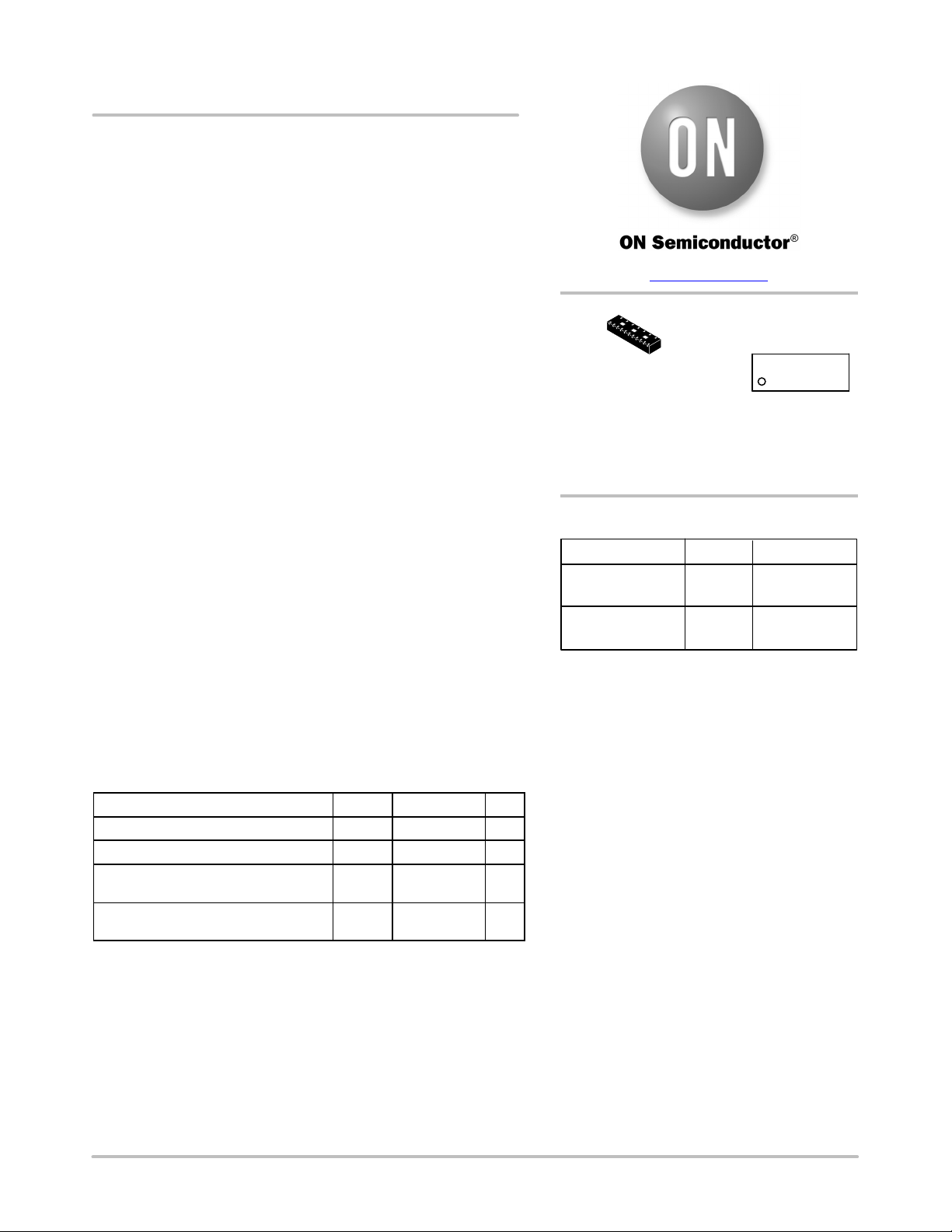
I/O
Pin 1
GND
Pin 3
I/O
Pin 2
I/O
Pin 4
GND
Pin 6
GND
Pin 9
I/O
Pin 5
I/O
Pin 7
GND
Pin 13
Note: Only Minimum of 1 GND connection required
I/O
Pin 8
GND
Pin 15
I/O
Pin 10
Pin 17
I/O
Pin 11
GND
=
Figure 1. Pin Schematic
I/O
I/O
GND
I/O
I/O
GND
I/O
I/O
GND
I/O
I/O
1
2
N/C
3
4
5
6
N/C
7
8
N/C
9
10
11
N/C
18
GND
17
16
N/C
15
GND
14
N/C
13
GND
12
N/C
Figure 2. Pin Configuration
Note: Only minimum of one pin needs to be connected to ground for functional-
ity of all pins. All pins labeled “N/C” should have no electrical connection.
www.onsemi.com
2
Page 3
ESD7008, SZESD7008
RWM
BR
R
C
C
V
C
J
= 25°C unless otherwise specified)
A
I/O Pin to GND (Note 1) 5.0 V
IT = 1 mA, I/O Pin to GND 5.5 6.7 V
V
= 5 V, I/O Pin to GND 1.0
RWM
IPP = 1 A, I/O Pin to GND (8 x 20 ms pulse)
IEC61000−4−2, ±8 kV Contact See Figures 3 and 4 V
IPP = ±8 A
I
= ±16 A
PP
13.2
18.2
VR = 0 V, f = 1 MHz between I/O Pins and GND 0.12 0.15 pF
VR = 0 V, f = 1 MHz between I/O Pins and GND 0.02 pF
J
ELECTRICAL CHARACTERISTICS (T
Parameter
Reverse Working Voltage V
Breakdown Voltage V
Reverse Leakage Current I
Clamping Voltage (Note 1) V
Clamping Voltage (Note 2) V
Clamping Voltage
TLP (Note 3)
See Figures 8 through 11
Junction Capacitance C
Junction Capacitance
Difference
Symbol Conditions Min Typ Max Unit
DC
1. Surge current waveform per Figure 7.
2. For test procedure see Figures 5 and 6 and application note AND8307/D.
3. ANSI/ESD STM5.5.1 − Electrostatic Discharge Sensitivity Testing using Transmission Line Pulse (TLP) Model.
TLP conditions: Z
= 50 W, tp = 100 ns, tr = 4 ns, averaging window; t1 = 30 ns to t2 = 60 ns.
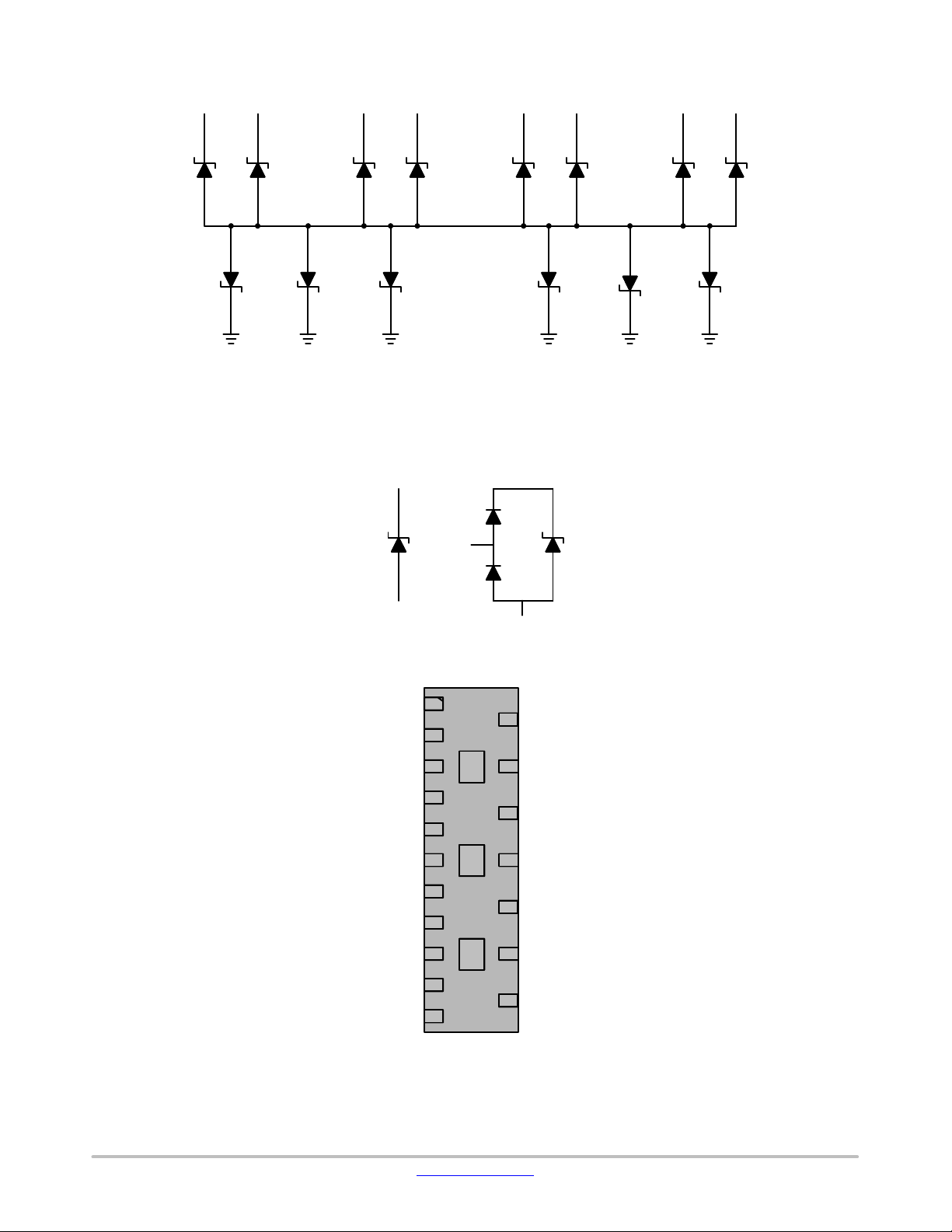
0
90
80
0
70
60
−10
50
40
30
VOLTAGE (V)
20
10
−20
−30
VOLTAGE (V)
−40
0
−10
−20 0 20 40 60 80 100 120 140
−50
−20 0 20 40 60 80 100 120 140
TIME (ns) TIME (ns)
Figure 3. IEC61000−4−2 +8 KV Contact
Clamping Voltage
Figure 4. IEC61000−4−2 −8 KV Contact
Clamping Voltage
mA
10 V
www.onsemi.com
3
Page 4
ESD7008, SZESD7008
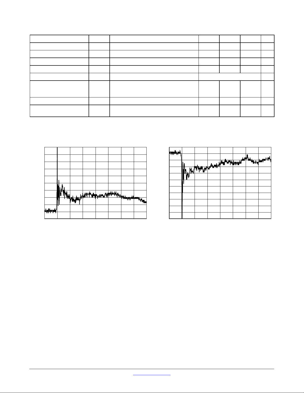
IEC 61000−4−2 Spec.
Test Volt-
Level
age (kV)
1 2 7.5 4 2
2 4 15 8 4
3 6 22.5 12 6
4 8 30 16 8
ESD Gun
First Peak
Current
(A)
Current at
30 ns (A)
Device
Under
Test
50 W
Cable
IEC61000−4−2 Waveform
I
peak
Current at
60 ns (A)
100%
90%
I @ 30 ns
I @ 60 ns
10%
Figure 5. IEC61000−4−2 Spec
Oscilloscope
50 W
tP = 0.7 ns to 1 ns
Figure 6. Diagram of ESD Clamping Voltage Test Setup
The following is taken from Application Note
AND8308/D − Interpretation of Datasheet Parameters
for ESD Devices.
ESD Voltage Clamping
For sensitive circuit elements it is important to limit the
voltage that an IC will be exposed to during an ESD event
to as low a voltage as possible. The ESD clamping voltage
is the voltage drop across the ESD protection diode during
an ESD event per the IEC61000−4−2 waveform. Since the
IEC61000−4−2 was written as a pass/fail spec for larger
100
t
r
90
80
70
60
50
40
30
20
% OF PEAK PULSE CURRENT
10
0
020406080
PEAK VALUE I
t
P
Figure 7. 8 x 20 ms Pulse Waveform
systems such as cell phones or laptop computers it is not
clearly defined in the spec how to specify a clamping voltage
at the device level. ON Semiconductor has developed a way
to examine the entire voltage waveform across the ESD
protection diode over the time domain of an ESD pulse in the
form of an oscilloscope screenshot, which can be found on
the datasheets for all ESD protection diodes. For more
information on how ON Semiconductor creates these
screenshots and how to interpret them please refer to
AND8307/D.
@ 8 ms
RSM
PULSE WIDTH (tP) IS DEFINED
AS THAT POINT WHERE THE
PEAK CURRENT DECAY = 8 ms
HALF VALUE I
t, TIME (ms)
/2 @ 20 ms
RSM
www.onsemi.com
4
Page 5

ESD7008, SZESD7008
22
20
18
16
14
12
10
8
CURRENT (A)
6
4
2
0
024681012141618
VOLTAGE (V)
Figure 8. Positive TLP I−V Curve Figure 9. Negative TLP I−V Curve
Transmission Line Pulse (TLP) Measurement
Transmission Line Pulse (TLP) provides current versus
voltage (I−V) curves in which each data point is obtained
from a 100 ns long rectangular pulse from a charged
transmission line. A simplified schematic of a typical TLP
system is shown in Figure 10. TLP I−V curves of ESD
protection devices accurately demonstrate the product’s
ESD capability because the 10s of amps current levels and
under 100 ns time scale match those of an ESD event. This
is illustrated in Figure 11 where an 8 kV IEC 61000−4−2
current waveform is compared with TLP current pulses at
8 A and 16 A. A TLP I−V curve shows the voltage at which
the device turns on as well as how well the device clamps
voltage over a range of current levels.
2220
−22
−20
−18
−16
−14
−12
−10
−8
CURRENT (A)
−6
−4
−2
0
024681012141618 2220
VOLTAGE (V)
L
Attenuator
S
50 W Coax
Cable
÷
50 W Coax
Cable
10 MW
V
C
Figure 10. Simplified Schematic of a Typical TLP
System
I
M
V
M
Oscilloscope
DUT
Figure 11. Comparison Between 8 kV IEC 61000−4−2 and 8 A and 16 A TLP Waveforms
www.onsemi.com
5
Page 6

ESD7008, SZESD7008
With ESD7008Without ESD
Figure 12. HDMI1.4 Eye Diagram with and without ESD7008. 3.4 Gb/s, 400 mV
PP
With ESD7008Without ESD
Figure 13. USB3.0 Eye Diagram with and without ESD7008. 5.0 Gb/s, 400 mV
With ESD7008Without ESD
PP
Figure 14. Thunderbolt Eye Diagram with and without ESD7008. 10 Gb/s, 400 mV
PP
www.onsemi.com
6
Page 7

ESD7008, SZESD7008
4
2
0
−2
−4
−6
S21 INSERTION LOSS (dB)
−8
−10
1.E+06 1.E+07 1.E+08 1.E+09 1.E+10
FREQUENCY (Hz)
Figure 15. ESD7008 Insertion Loss
ESD7008
IO−GND
USB 3.0 Type A
ESD7008
Connector
StdA_SSTX+
Vbus
N/ C
N/ C
N/ C
N/ C
N/C
N/C
N/C
StdA_SSTX−
D−
Vbus
GND_DRAIN
Iden or N/C
D+
StdA_SSRX+
GND
StdA_SSRX−
Figure 16. USB3.0 Layout Diagram
www.onsemi.com
7
Page 8

CONFIG 1
ESD9X
ESD7008
ESD7008, SZESD7008
AUX_CH+
Thunderbolt
Connector
GND
Hot Plug Detect
D3−
CONFIG1
D3+
CONFIG2
GND
GND
D2−
D0−
D2+
D0+
GND
GND
D1−
AUX_CH+
D1+
AUX_CH−
GND
DP_PWR
CONFIG 2
NUP4114
Figure 17. Thunderbolt Layout Diagram
www.onsemi.com
8
Page 9

ESD7008, SZESD7008
ESD7008
HDMI
Type A Connector
D2+
GND
D2−
D1+
GND
D1−
D0+
GND
D0−
CLK +
GND
CLK −
CEC
N/C ( or HEC _ DAT – HDMI 1.4 )
SCL
SDA
GND
5V
HPD ( and HEC _DAT – HDMI 1.4)
NUP4114
Figure 18. HDMI Layout Diagram
ESD7008
Timing Controller
Figure 19. V−by−One HS Layout Diagram (for LCD Panel)
Connector
V−by−One HS
www.onsemi.com
9
Page 10

MECHANICAL CASE OUTLINE
PACKAGE DIMENSIONS
18
1
SCALE 2:1
B
A
E
(A3)
A
A1
C
D2
11
E2
REFERENCE
2X
2X
NOTE 4
PIN ONE
0.10 C
0.10 C
0.05 C
0.10 C
DETAIL A
D
TOP VIEW
DETAIL B
SIDE VIEW
eA
1
UDFN18, 5.5x1.5, 0.5P
CASE 517BV
ISSUE A
LL2
L1
DETAIL A
OPTIONAL
CONSTRUCTIONS
SEATING
PLANE
NOTE 5
DETAIL B
OPTIONAL
CONSTRUCTION
DATE 11 DEC 2012
NOTES:
L
1. DIMENSIONING AND TOLERANCING PER
ASME Y14.5M, 1994.
2. CONTROLLING DIMENSION: MILLIMETERS.
3. DIMENSION b APPLIES TO PLATED
TERMINAL AND IS MEASURED BETWEEN
0.10 AND 0.20 MM FROM TERMINAL TIP.
4. COPLANARITY APPLIES TO THE EXPOSED
PAD AS WELL AS THE TERMINALS.
5. EXPOSED ENDS OF TERMINALS ARE
ELECTRICALLY ACTIVE.
MILLIMETERS
MOLD CMPDEXPOSED Cu
DIM MIN MAX
A 0.45 0.55
A1 0.00 0.05
A3 0.13 REF
b 0.15 0.25
D 5.50 BSC
D2 0.45 0.55
E 1.50 BSC
E2 0.35 0.45
eA 0.50 BSC
eB 0.75 BSC
L 0.20 0.40
L1 0.00 0.05
L2 0.10 REF
eB
BOTTOM VIEW
1218
18X
L
b
M
0.10 B
NOTE 3
M
0.05ACC
RECOMMENDED
SOLDERING FOOTPRINT*
1.50
PITCH
3X
0.60
3X
0.50
0.50
PITCH
*For additional information on our Pb−Free strategy and soldering
details, please download the ON Semiconductor Soldering and
Mounting Techniques Reference Manual, SOLDERRM/D.
0.75
PITCH
18X
0.50
1.80
18X
0.30
DIMENSION: MILLIMETERS
END VIEW
GENERIC
MARKING DIAGRAM*
XXXXM
G
XXXX = Specific Device Code
M = Date Code
G = Pb−Free Package
*This information is generic. Please refer
to device data sheet for actual part
marking.
DOCUMENT NUMBER:
DESCRIPTION:
ON Semiconductor and are trademarks of Semiconductor Components Industries, LLC dba ON Semiconductor or its subsidiaries in the United States and/or other countries.
ON Semiconductor reserves the right to make changes without further notice to any products herein. ON Semiconductor makes no warranty, representation or guarantee regarding
the suitability of its products for any particular purpose, nor does ON Semiconductor assume any liability arising out of the application or use of any product or circuit, and specifically
disclaims any and all liability, including without limitation special, consequential or incidental damages. ON Semiconductor does not convey any license under its patent rights nor the
rights of others.
© Semiconductor Components Industries, LLC, 2019
98AON55750E
UDFN18, 5.5X1.5, 0.5P
Electronic versions are uncontrolled except when accessed directly from the Document Repository.
Printed versions are uncontrolled except when stamped “CONTROLLED COPY” in red.
PAGE 1 OF 1
www.onsemi.com
Page 11

ON Semiconductor and are trademarks of Semiconductor Components Industries, LLC dba ON Semiconductor or its subsidiaries in the United States and/or other countries.
ON Semiconductor owns the rights to a number of patents, trademarks, copyrights, trade secrets, and other intellectual property. A listing of ON Semiconductor’s product/patent
coverage may be accessed at www.onsemi.com/site/pdf/Patent−Marking.pdf
ON Semiconductor makes no warranty, representation or guarantee regarding the suitability of its products for any particular purpose, nor does ON Semiconductor assume any liability
arising out of the application or use of any product or circuit, and specifically disclaims any and all liability, including without limitation special, consequential or incidental damages.
Buyer is responsible for its products and applications using ON Semiconductor products, including compliance with all laws, regulations and safety requirements or standards,
regardless of any support or applications information provided by ON Semiconductor. “Typical” parameters which may be provided in ON Semiconductor data sheets and/or
specifications can and do vary in different applications and actual performance may vary over time. All operating parameters, including “Typicals” must be validated for each customer
application by customer’s technical experts. ON Semiconductor does not convey any license under its patent rights nor the rights of others. ON Semiconductor products are not
designed, intended, or authorized for use as a critical component in life support systems or any FDA Class 3 medical devices or medical devices with a same or similar classification
in a foreign jurisdiction or any devices intended for implantation in the human body. Should Buyer purchase or use ON Semiconductor products for any such unintended or unauthorized
application, Buyer shall indemnify and hold ON Semiconductor and its officers, employees, subsidiaries, affiliates, and distributors harmless against all claims, costs, damages, and
expenses, and reasonable attorney fees arising out of, directly or indirectly, any claim of personal injury or death associated with such unintended or unauthorized use, even if such
claim alleges that ON Semiconductor was negligent regarding the design or manufacture of the part. ON Semiconductor is an Equal Opportunity/Affirmative Action Employer. This
literature is subject to all applicable copyright laws and is not for resale in any manner.
. ON Semiconductor reserves the right to make changes without further notice to any products herein.
PUBLICATION ORDERING INFORMATION
LITERATURE FULFILLMENT:
Email Requests to: orderlit@onsemi.com
ON Semiconductor Website: www.onsemi.com
TECHNICAL SUPPORT
North American Technical Support:
Voice Mail: 1 800−282−9855 Toll Free USA/Canada
Phone: 011 421 33 790 2910
Europe, Middle East and Africa Technical Support:
Phone: 00421 33 790 2910
For additional information, please contact your local Sales Representative
◊
www.onsemi.com
1
 Loading...