

DTA114EET1 SERIES
Preferred Devices
Bias Resistor Transistor
PNP Silicon Surface Mount Transistor
with Monolithic Bias Resistor Network
This new series of digital transistors is designed to replace a single
device and its external resistor bias network. The BRT (Bias Resistor
Transistor) contains a single transistor with a monolithic bias network
consisting of two resistors; a series base resistor and a base–emitter
resistor. The BRT eliminates these individual components by
integrating them into a single device. The use of a BRT can reduce
both system cost and board space. The device is housed in the
SC–75/SOT–416 package which is designed for low power surface
mount applications.
• Simplifies Circuit Design
• Reduces Board Space
• Reduces Component Count
• The SC–75/SOT–416 package can be soldered using
wave or reflow. The modified gull–winged leads absorb
thermal stress during soldering eliminating the possibility
of damage to the die.
• Available in 8 mm, 7 inch/3000 Unit Tape & Reel
http://onsemi.com
PNP SILICON
BIAS RESISTOR
TRANSISTORS
COLLECTOR
3
1
BASE
2
EMITTER
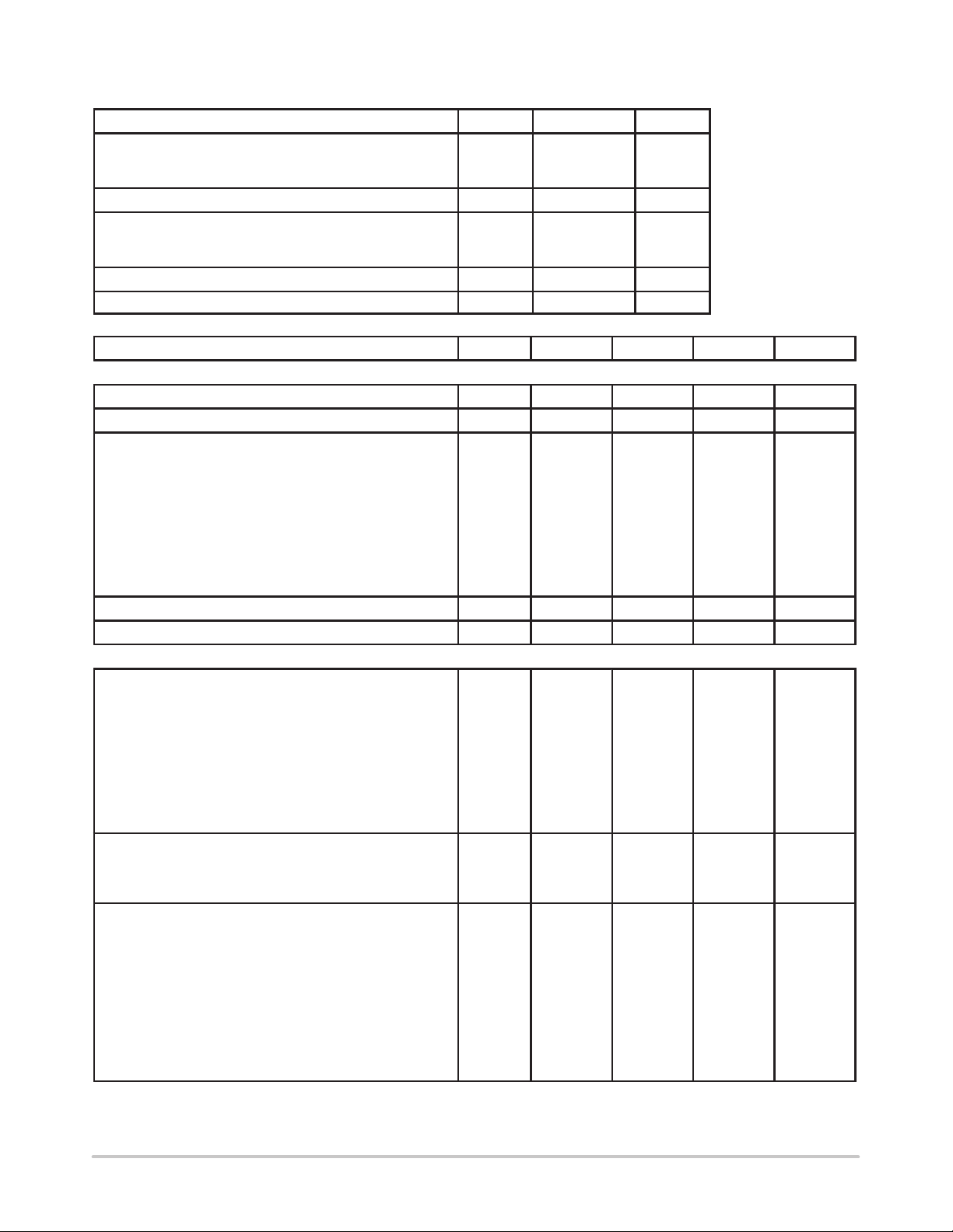
MAXIMUM RATINGS (T
Rating
Collector-Base Voltage V
Collector-Emitter Voltage V
Collector Current I
= 25°C unless otherwise noted)
A
Symbol Value Unit
CBO
CEO
C
DEVICE MARKING AND RESISTOR VALUES
Device Marking R1 (K) R2 (K) Shipping
DTA114EET1
DTA124EET1
DTA144EET1
DTA114YET1
DTA114TET1
DTA143TET1
DTA123EET1
DTA143ZET1
DTA124XET1
DTA123JET1
6A
6B
6C
6D
6E
6F
6H
6K
6L
6M
10
22
47
10
10
4.7
2.2
4.7
22
2.2
10
22
47
47
∞
∞
2.2
47
47
47
50 Vdc
50 Vdc
100 mAdc
3000/Tape & Reel
3
2
1
CASE 463
SOT–416/SC–75
STYLE 1
Preferred devices are recommended choices for future use
and best overall value.
Semiconductor Components Industries, LLC, 2000
May, 2000 – Rev. 0
1 Publication Order Number:
DTA114EET1/D
DTA114EET1 SERIES
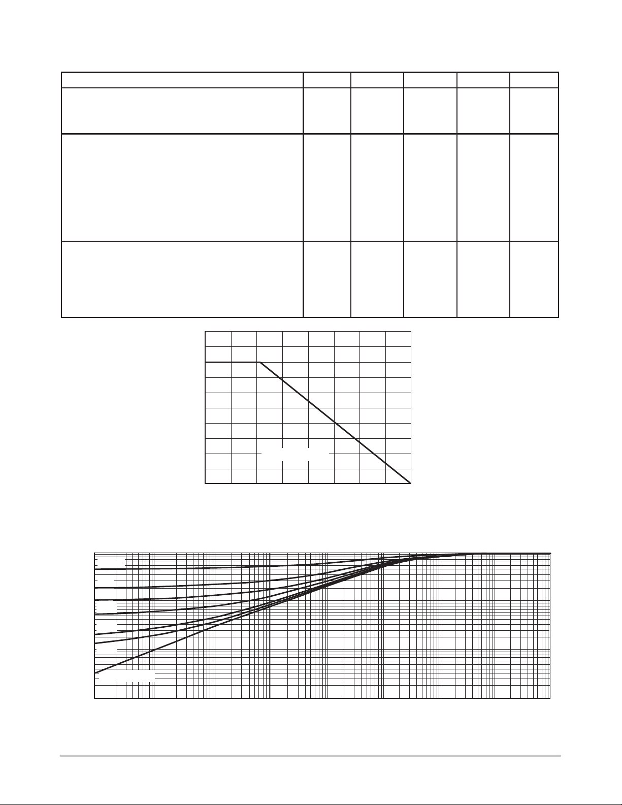
THERMAL CHARACTERISTICS
Characteristic Symbol Max Unit
Total Device Dissipation,
FR–4 Board
Derate above 25°C
Thermal Resistance, Junction to Ambient
Total Device Dissipation,
FR–4 Board
Derate above 25°C
Thermal Resistance, Junction to Ambient
Junction and Storage Temperature Range TJ, T
ELECTRICAL CHARACTERISTICS (T
OFF CHARACTERISTICS
Collector–Base Cutoff Current (VCB = 50 V, IE = 0) I
Collector–Emitter Cutoff Current (VCE = 50 V, IB = 0) I
Emitter–Base Cutoff Current DTA114EET1
(V
EB
Collector–Base Breakdown Voltage (IC = 10 µA, IE = 0) V
Collector–Emitter Breakdown Voltage
ON CHARACTERISTICS
DC Current Gain DTA114EET1
(V
CE
Collector–Emitter Saturation Voltage (IC = 10 mA, IE = 0.3 mA)
(I
= 10 mA, IB = 5 mA) DTA123EET1
C
= 10 mA, IB = 1 mA) DTA114TET1/DTA143TET1/
(I
C
DTA143ZET1/DTA124XET1
Output Voltage (on)
(V
CC
(V
CC
1. FR–4 @ Minimum Pad
2. FR–4 @ 1.0 × 1.0 Inch Pad
3. Pulse Test: Pulse Width < 300 µs, Duty Cycle < 2.0%
(1.)
@ TA = 25°C
(1.)
(2.)
@ TA = 25°C
(2.)
= 25°C unless otherwise noted)
A
Characteristic
= 6.0 V, IC = 0) DTA124EET1
DTA144EET1
DTA114YET1
DTA114TET1
DTA143TET1
DTA123EET1
DTA143ZET1
DTA124XET1
DTA123JET1
(3.)
(IC = 2.0 mA, IB = 0) V
(3.)
= 10 V, IC = 5.0 mA) DTA124EET1
DTA144EET1
DTA114YET1
DTA114TET1
DTA143TET1
DTA123EET1
DTA143ZET1
DTA124XET1
DTA123JET1
= 5.0 V, VB = 2.5 V, RL = 1.0 kΩ) DTA114EET1
DTA124EET1
DTA114YET1
DTA114TET1
DTA143TET1
DTA123EET1
DTA143ZET1
DTA124XET1
DTA123JET1
= 5.0 V, VB = 3.5 V, RL = 1.0 kΩ) DTA144EET1
P
D
R
θ
JA
P
D
R
θ
JA
stg
200
1.6
mW
mW/°C
600 °C/W
300
2.4
mW
mW/°C
400 °C/W
–55 to +150 °C
Symbol Min Typ Max Unit
CBO
CEO
I
EBO
(BR)CBO
(BR)CEO
h
FE
V
CE(sat)
V
OL
— — 100 nAdc
— — 500 nAdc
—
—
—
—
—
—
—
—
—
—
—
—
—
—
—
—
—
—
—
—
0.5
0.2
0.1
0.2
0.9
1.9
2.3
0.18
0.13
0.2
mAdc
50 — — Vdc
50 — — Vdc
35
60
80
80
160
160
8.0
80
80
80
60
100
140
140
250
250
15
140
130
140
—
—
—
—
—
—
—
—
—
—
— — 0.25 Vdc
Vdc
—
—
—
—
—
—
—
—
—
—
—
—
—
—
—
—
—
—
—
—
0.2
0.2
0.2
0.2
0.2
0.2
0.2
0.2
0.2
0.2
http://onsemi.com
2
DTA114EET1 SERIES
ELECTRICAL CHARACTERISTICS (T
= 25°C unless otherwise noted) (Continued)
A
Characteristic
Output Voltage (of f) (VCC = 5.0 V, VB = 0.5 V, RL = 1.0 kΩ)
(V
= 5.0 V, VB = 0.050 V, RL = 1.0 kΩ) DTA114TET1
CC
= 5.0 V, VB = 0.25 V, RL = 1.0 kΩ) DTA143TET1
(V
CC
DTA123EET1
Input Resistor DTA114EET1
DTA124EET1
DTA144EET1
DTA114YET1
DTA114TET1
DTA143TET1
DTA123EET1
DTA143ZET1
DTA124XET1
DTA123JET1
Resistor Ratio DTA114EET1/DTA124EET1/DTA144EET1
DTA114YET1
DTA114TET1/DTA143TET1
DTA123EET1
DTA143ZET1
DTA124XET1
DTA123JET1
250
Symbol Min Typ Max Unit
V
OH
R1 7.0
R1/R
2
4.9 — — Vdc
15.4
32.9
7.0
7.0
3.3
1.5
3.3
15.4
1.54
0.8
0.17
—
0.8
0.055
0.38
0.038
10
22
47
10
10
4.7
2.2
4.7
22
2.2
1.0
0.21
—
1.0
0.1
0.47
0.047
13
28.6
61.1
13
13
6.1
2.9
6.1
28.6
2.86
1.2
0.25
—
1.2
0.185
0.56
0.056
kΩ
1.0
0.1
0.01
D = 0.5
0.2
0.1
0.05
0.02
0.01
200
150
100
R
50
, POWER DISSIPATION (MILLIWATTS)
D
P
0
–50 0 50 100 150
= 600°C/W
θ
JA
T
, AMBIENT TEMPERATURE (°C)
A
Figure 1. Derating Curve
SINGLE PULSE
0.001
0.00001 0.0001 0.001 0.01 0.1 1.0 10 100 1000
r(t), NORMALIZED TRANSIENT THERMAL RESISTANCE
t, TIME (s)
Figure 2. Normalized Thermal Response
http://onsemi.com
3
DTA114EET1 SERIES
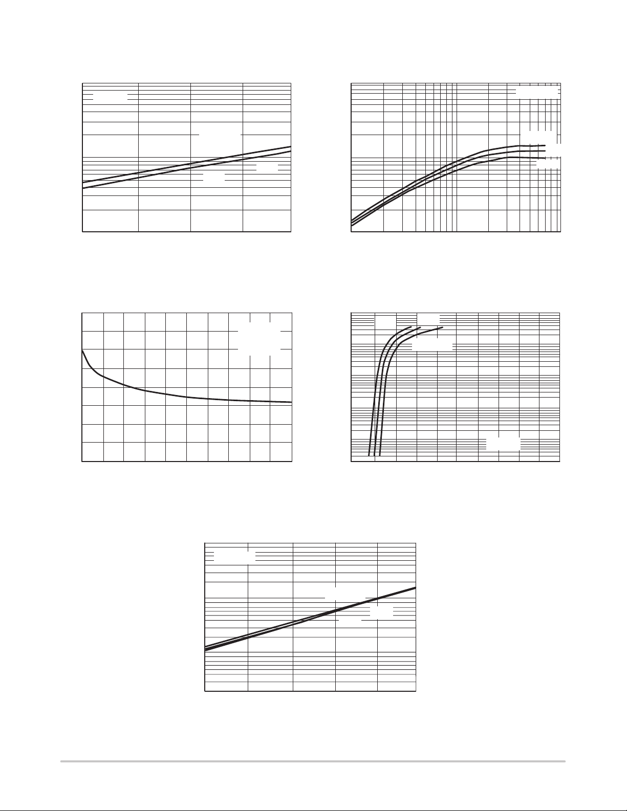
TYPICAL ELECTRICAL CHARACTERISTICS — DTA114EET1
1
IC/IB = 10
TA= –25°C
0.1
75°C
, MAXIMUM COLLECTOR VOLTAGE (VOLTS)
0.01
CE(sat)
V
040
4
3
2
20
, COLLECTOR CURRENT (mA)
I
C
Figure 3. V
CE(sat)
versus I
C
f = 1 MHz
l
= 0 V
E
= 25°C
T
A
25°C
50
1000
100
, DC CURRENT GAIN (NORMALIZED)
FE
10
100
10
1
VCE = 10 V
TA=75°C
25°C
–25°C
1 10 100
IC, COLLECTOR CURRENT (mA)
Figure 4. DC Current Gain
75°C
25°C
TA= –25°C
, CAPACITANCE (pF)
ob
1
C
0
010203040
V
, REVERSE BIAS VOLTAGE (VOLTS)
R
Figure 5. Output Capacitance Figure 6. Output Current versus Input Voltage
100
VO = 0.2 V
10
1
, INPUT VOLTAGE (VOLTS)
in
V
0.1
0
Figure 7. Input Voltage versus Output Current
0.1
, COLLECTOR CURRENT (mA) h
C
0.01
I
50
10 20 30 40 50
, COLLECTOR CURRENT (mA)
I
C
0.001
0
TA= –25°C
75°C
12345
V
25°C
678910
, INPUT VOLTAGE (VOLTS)
in
VO = 5 V
http://onsemi.com
4

DTA114EET1 SERIES
V
,
MA
IM
M
COLLECTOR
VOLTAGE
VOLTS)
C
,
CA
ACITA
CE
F)
TYPICAL ELECTRICAL CHARACTERISTICS — DTA124EET1
10
(
IC/IB = 10
1000
1
TA= –25°C
U
0.1
X
0.01
CE(sat)
020 50
, COLLECTOR CURRENT (mA)
I
C
Figure 8. V
CE(sat)
versus I
4
25°C
100
75°C
, DC CURRENT GAIN (NORMALIZED)
FE
10
40
C
100
f = 1 MHz
l
= 0 V
E
3
= 25°C
T
A
(p
N
2
P
ob
1
0
010203040
V
, REVERSE BIAS VOLTAGE (VOLTS)
R
, COLLECTOR CURRENT (mA) h
C
I
0.01
0.001
50
Figure 10. Output Capacitance
VCE = 10 V
TA=75°C
1
I
, COLLECTOR CURRENT (mA)
C
10
Figure 9. DC Current Gain
25°C
75°C
TA= –25°C
10
1
0.1
01 2 3 4
V
, INPUT VOLTAGE (VOLTS)
in
5678910
Figure 11. Output Current versus Input Voltage
25°C
–25°C
100
VO = 5 V
100
VO = 0.2 V
TA= –25°C
10
25°C
75°C
, INPUT VOLTAGE (VOLTS)
1
in
V
0.1
0 10 20 30
IC, COLLECTOR CURRENT (mA)
Figure 12. Input Voltage versus Output Current
http://onsemi.com
5
40 50

DTA114EET1 SERIES
V
,
MA
IM
M
COLLECTOR
VOLTAGE
VOLTS)
TYPICAL ELECTRICAL CHARACTERISTICS — DTA144EET1
1
(
U
X
IC/IB = 10
TA= –25°C
0.1
0.01
CE(sat)
010203040
IC, COLLECTOR CURRENT (mA)
Figure 13. V
1
0.8
0.6
CE(sat)
versus I
75°C
25°C
C
f = 1 MHz
l
= 0 V
E
= 25°C
T
A
1000
TA=75°C
100
, DC CURRENT GAIN (NORMALIZED)
FE
10
1 10 100
, COLLECTOR CURRENT (mA)
I
C
Figure 14. DC Current Gain
100
10
1
TA=75°C
25°C
–25°C
25°C
–25°C
0.4
, CAPACITANCE (pF)
ob
C
0.2
0
010203040
, REVERSE BIAS VOLTAGE (VOLTS)
V
R
Figure 15. Output Capacitance Figure 16. Output Current versus Input Voltage
100
TA= –25°C
10
1
, INPUT VOLTAGE (VOLTS)
in
V
0.1
010203040
0.1
0.01
, COLLECTOR CURRENT (mA) h
C
I
0.001
50
75°C
IC, COLLECTOR CURRENT (mA)
010
25°C
VO = 5 V
123456789
Vin, INPUT VOLTAGE (VOLTS)
VO = 0.2 V
50
Figure 17. Input Voltage versus Output Current
http://onsemi.com
6

DTA114EET1 SERIES
V
,
I
T
VOLTAGE
VOLTS)
V
,
MA
IM
M
COLLECTOR
VOLTAGE
VOLTS)
C
,
CA
ACITA
CE
F)
TYPICAL ELECTRICAL CHARACTERISTICS — DTA114YET1
1
(
U
X
CE(sat)
0.001
(p
N
P
ob
IC/IB = 10
0.1
0.01
020406080
IC, COLLECTOR CURRENT (mA)
Figure 18. V
4.5
4
3.5
3
2.5
2
1.5
1
0.5
0
0 2 4 6 8101520253035404550
, REVERSE BIAS VOLTAGE (VOLTS)
V
R
CE(sat)
TA= –25°C
75°C
versus I
C
f = 1 MHz
l
= 0 V
E
= 25°C
T
A
25°C
Figure 20. Output Capacitance Figure 21. Output Current versus Input Voltage
180
VCE = 10 V
160
140
120
100
80
60
40
, DC CURRENT GAIN (NORMALIZED)
20
FE
0
2 4 6 8 15 20 40 50 60 70 80 90
1 10 100
IC, COLLECTOR CURRENT (mA)
–25°C
TA=75°C
25°C
Figure 19. DC Current Gain
100
TA=75°C
–25°C
10
, COLLECTOR CURRENT (mA) h
C
I
1
0 246810
Vin, INPUT VOLTAGE (VOLTS)
VO = 5 V
25°C
(
NPU
in
10
VO = 0.2 V
75°C
1
0.1
01020304050
IC, COLLECTOR CURRENT (mA)
25°C
TA= –25°C
Figure 22. Input Voltage versus Output Current
http://onsemi.com
+12 V
T ypical Application
for PNP BRTs
LOAD
Figure 23. Inexpensive, Unregulated Current Source
7

DTA114EET1 SERIES
MINIMUM RECOMMENDED FOOTPRINTS FOR SURFACE MOUNTED APPLICATIONS
Surface mount board layout is a critical portion of the
total design. The footprint for the semiconductor packages
must be the correct size to insure proper solder connection
TYPICAL
SOLDERING PATTERN
Unit: mm
0.5 min. (3x)
SOT–416/SC–75 POWER DISSIPATION
The power dissipation of the SOT–416/SC–75 is a
function of the pad size. This can vary from the minimum
pad size for soldering to the pad size given for maximum
power dissipation. Power dissipation for a surface mount
device is determined by T
junction temperature of the die, R
, the maximum rated
J(max)
, the thermal
JA
θ
resistance from the device junction to ambient; and the
operating temperature, TA. Using the values provided on
the data sheet, P
can be calculated as follows:
D
T
– T
PD =
J(max)
A
R
θ
JA
The values for the equation are found in the maximum
ratings table on the data sheet. Substituting these values
interface between the board and the package. With the
correct pad geometry, the packages will self align when
subjected to a solder reflow process.
0.5 min. (3x)
0.5
1
1.4
into the equation for an ambient temperature T
one can calculate the power dissipation of the device which
in this case is 200 milliwatts.
150°C – 25°C
PD =
600°C/W
= 200 milliwatts
The 600°C/W assumes the use of the recommended
footprint on a glass epoxy printed circuit board to achieve a
power dissipation of 200 milliwatts. Another alternative
would be to use a ceramic substrate or an aluminum core
board such as Thermal Clad. Using a board material such
as Thermal Clad, a higher power dissipation can be
achieved using the same footprint.
of 25°C,
A
SOLDERING PRECAUTIONS
The melting temperature of solder is higher than the rated
temperature of the device. When the entire device is heated
to a high temperature, failure to complete soldering within
a short time could result in device failure. Therefore, the
following items should always be observed in order to
minimize the thermal stress to which the devices are
subjected.
• Always preheat the device.
• The delta temperature between the preheat and
soldering should be 100°C or less.*
• When preheating and soldering, the temperature of the
leads and the case must not exceed the maximum
temperature ratings as shown on the data sheet. When
using infrared heating with the reflow soldering
method, the difference should be a maximum of 10°C.
http://onsemi.com
• The soldering temperature and time should not exceed
260°C for more than 10 seconds.
• When shifting from preheating to soldering, the
maximum temperature gradient should be 5°C or less.
• After soldering has been completed, the device should
be allowed to cool naturally for at least three minutes.
Gradual cooling should be used as the use of forced
cooling will increase the temperature gradient and
result in latent failure due to mechanical stress.
• Mechanical stress or shock should not be applied
during cooling.
* Soldering a device without preheating can cause
excessive thermal shock and stress which can result in
damage to the device.
8

DTA114EET1 SERIES
SOLDER STENCIL GUIDELINES
Prior to placing surface mount components onto a printed
circuit board, solder paste must be applied to the pads. A
solder stencil is required to screen the optimum amount of
solder paste onto the footprint. The stencil is made of brass
TYPICAL SOLDER HEATING PROFILE
For any given circuit board, there will be a group of
control settings that will give the desired heat pattern. The
operator must set temperatures for several heating zones,
and a figure for belt speed. Taken together, these control
settings make up a heating “profile” for that particular
circuit board. On machines controlled by a computer, the
computer remembers these profiles from one operating
session to the next. Figure 24 shows a typical heating
profile for use when soldering a surface mount device to a
printed circuit board. This profile will vary among
soldering systems but it is a good starting point. Factors that
can affect the profile include the type of soldering system in
use, density and types of components on the board, type of
solder used, and the type of board or substrate material
being used. This profile shows temperature versus time.
200°C
150°C
100°C
STEP 1
PREHEAT
ZONE 1
“RAMP”
DESIRED CURVE FOR HIGH
STEP 2
VENT
“SOAK”
MASS ASSEMBLIES
ZONES 2 & 5
150°C
100°C
STEP 3
HEATING
“RAMP”
or stainless steel with a typical thickness of 0.008 inches.
The stencil opening size for the surface mounted package
should be the same as the pad size on the printed circuit
board, i.e., a 1:1 registration.
The line on the graph shows the actual temperature that
might be experienced on the surface of a test board at or
near a central solder joint. The two profiles are based on a
high density and a low density board. The Vitronics
SMD310 convection/infrared reflow soldering system was
used to generate this profile. The type of solder used was
62/36/2 Tin Lead Silver with a melting point between
177–189°C. When this type of furnace is used for solder
reflow work, the circuit boards and solder joints tend to
heat first. The components on the board are then heated by
conduction. The circuit board, because it has a large surface
area, absorbs the thermal energy more efficiently, then
distributes this energy to the components. Because of this
effect, the main body of a component may be up to 30
degrees cooler than the adjacent solder joints.
STEP 4
HEATING
ZONES 3 & 6
“SOAK”
160°C
140°C
STEP 5
HEATING
ZONES 4 & 7
“SPIKE”
170°C
SOLDER IS LIQUID FOR
40 TO 80 SECONDS
(DEPENDING ON
MASS OF ASSEMBLY)
STEP 6
VENT
205° TO 219°C
SOLDER JOINT
STEP 7
COOLING
PEAK AT
50°C
TIME (3 TO 7 MINUTES TOTAL)
DESIRED CURVE FOR LOW
MASS ASSEMBLIES
Figure 24. T ypical Solder Heating Profile
http://onsemi.com
9
T
MAX

S
3 PL
D
0.20 (0.008) B
M
J
–A–
3
DTA114EET1 SERIES
P ACKAGE DIMENSIONS
SC–75
(SOT–416)
CASE 463–01
ISSUE B
2
G
–B–
1
0.20 (0.008) A
K
C
NOTES:
1. DIMENSIONING AND TOLERANCING PER ANSI
Y14.5M, 1982.
2. CONTROLLING DIMENSION: MILLIMETER.
DIM MIN MAX MIN MAX
A 0.70 0.80 0.028 0.031
B 1.40 1.80 0.055 0.071
C 0.60 0.90 0.024 0.035
D 0.15 0.30 0.006 0.012
G 1.00 BSC 0.039 BSC
H ––– 0.10 ––– 0.004
J 0.10 0.25 0.004 0.010
K 1.45 1.75 0.057 0.069
L 0.10 0.20 0.004 0.008
S 0.50 BSC 0.020 BSC
INCHESMILLIMETERS
STYLE 1:
PIN 1. BASE
2. EMITTER
3. COLLECTOR
L
H
STYLE 2:
PIN 1. ANODE
2. N/C
3. CATHODE
STYLE 3:
PIN 1. ANODE
2. ANODE
3. CATHODE
STYLE 4:
PIN 1. CATHODE
2. CATHODE
3. ANODE
http://onsemi.com
10

Notes
DTA114EET1 SERIES
http://onsemi.com
11

DTA114EET1 SERIES
Thermal Clad is a trademark of the Bergquist Company
ON Semiconductor and are trademarks of Semiconductor Components Industries, LLC (SCILLC). SCILLC reserves the right to make changes
without further notice to any products herein. SCILLC makes no warranty , representation or guarantee regarding the suitability of its products for any particular
purpose, nor does SCILLC assume any liability arising out of the application or use of any product or circuit, and specifically disclaims any and all liability ,
including without limitation special, consequential or incidental damages. “Typical” parameters which may be provided in SCILLC data sheets and/or
specifications can and do vary in different applications and actual performance may vary over time. All operating parameters, including “Typicals” must be
validated for each customer application by customer’s technical experts. SCILLC does not convey any license under its patent rights nor the rights of others.
SCILLC products are not designed, intended, or authorized for use as components in systems intended for surgical implant into the body, or other applications
intended to support or sustain life, or for any other application in which the failure of the SCILLC product could create a situation where personal injury or
death may occur. Should Buyer purchase or use SCILLC products for any such unintended or unauthorized application, Buyer shall indemnify and hold
SCILLC and its officers, employees, subsidiaries, affiliates, and distributors harmless against all claims, costs, damages, and expenses, and reasonable
attorney fees arising out of, directly or indirectly , any claim of personal injury or death associated with such unintended or unauthorized use, even if such claim
alleges that SCILLC was negligent regarding the design or manufacture of the part. SCILLC is an Equal Opportunity/Affirmative Action Employer .
PUBLICATION ORDERING INFORMATION
NORTH AMERICA Literature Fulfillment:
Literature Distribution Center for ON Semiconductor
P.O. Box 5163, Denver, Colorado 80217 USA
Phone: 303–675–2175 or 800–344–3860 Toll Free USA/Canada
Fax: 303–675–2176 or 800–344–3867 Toll Free USA/Canada
Email: ONlit@hibbertco.com
Fax Response Line: 303–675–2167 or 800–344–3810 T oll Free USA/Canada
N. American Technical Support: 800–282–9855 Toll Free USA/Canada
EUROPE: LDC for ON Semiconductor – European Support
German Phone: (+1) 303–308–7140 (M–F 1:00pm to 5:00pm Munich Time)
Email: ONlit–german@hibbertco.com
French Phone: (+1) 303–308–7141 (M–F 1:00pm to 5:00pm Toulouse T ime)
Email: ONlit–french@hibbertco.com
English Phone: (+1) 303–308–7142 (M–F 12:00pm to 5:00pm UK Time)
Email: ONlit@hibbertco.com
EUROPEAN TOLL–FREE ACCESS*: 00–800–4422–3781
*Available from Germany, France, Italy, England, Ireland
CENTRAL/SOUTH AMERICA:
Spanish Phone: 303–308–7143 (Mon–Fri 8:00am to 5:00pm MST)
Email: ONlit–spanish@hibbertco.com
ASIA/PACIFIC : LDC for ON Semiconductor – Asia Support
Phone: 303–675–2121 (Tue–Fri 9:00am to 1:00pm, Hong Kong Time)
T oll Free from Hong Kong & Singapore:
001–800–4422–3781
Email: ONlit–asia@hibbertco.com
JAPAN: ON Semiconductor, Japan Customer Focus Center
4–32–1 Nishi–Gotanda, Shinagawa–ku, T okyo, Japan 141–0031
Phone: 81–3–5740–2745
Email: r14525@onsemi.com
ON Semiconductor Website: http://onsemi.com
For additional information, please contact your local
Sales Representative.
http://onsemi.com
12
DTA1 14EET1/D
 Loading...